

Philips ta8184p DATASHEETS
TOSHIBA Bipolar Linear Integrated Circuit Silicon Monolithic
TA8184P,TA8184F
Dual Channel Voltage/Tone Control IC
The TA8184P, TA8184F is DC controlled dual volume, balance,
tone (Bass and treble) IC.
It is suitable for car stereo, radio cassette, music center, TV
multiplex sound receiver and remote controlled applications.
Features
· Dual channel
· Wide volume control range
: Maximum attenuation ATT = 100dB (typ.)
(Vol. → Min, V
· Wide tone control range
: Bass V
: Treble VT = +12.5~−12.5dB (typ.), (f = 10 kHz)
· Built in loudness control
· Operating supply voltage range
: V
: V
CC (opr)
CC (opr)
B
= 7.5~15 V (TA8184P) (Ta = 25°C)
= 7.5~12.5 V (TA8184F) (Ta = 25°C)
= 1 Vrms, BW = 400 Hz~30 kHz)
IN
= +12.5~−12.5dB (typ.), (f = 100 Hz)
TA8184P
TA8184F
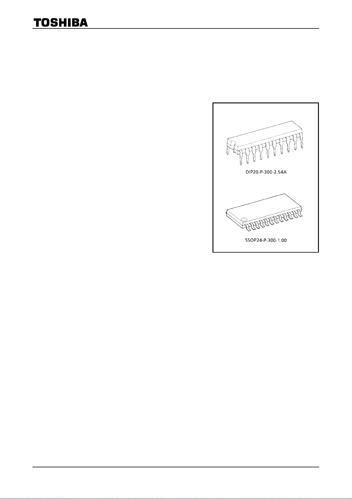
Weight
DIP20-P-300-2.54A: 1.4 g (typ.)
SSOP24-P-300-1.00: 0.31 g (typ.)
TA8184P/F
1
2002-03-05
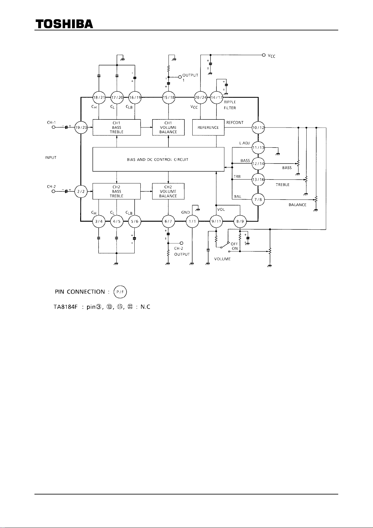
Block Diagram
TA8184P/F
2
2002-03-05
TA8184P/F
Pin Connection
(TA8184P)
Pin Function
Pin No. Symbol Explanation Pin No. Symbol Explanation
1 GND GND 11 L.ADJ. Loudness adjust
2 IN2 CH2, input 12 BASS Bass control
3 C
4 C
5 C
6 OUT2 CH2, output 16 C
7 BAL Balance control 17 C
8 VOL Volume control 18 C
9 LOUD Loudness switch 19 IN1 CH1, input
10 REF Reference 20 V
H (2)
L (2)
LB (2)
CH2, treble control time constant 13 TRBL Treble control
CH2, bass control time constant 14 RIP Ripple filter
CH2, bass control time constant 15 OUT1 CH1, output
LB (1)
L (1)
H (1)
CC
CH1, bass control time constant
CH1, bass control time constant
CH1, treble control time constant
VCC
3
2002-03-05
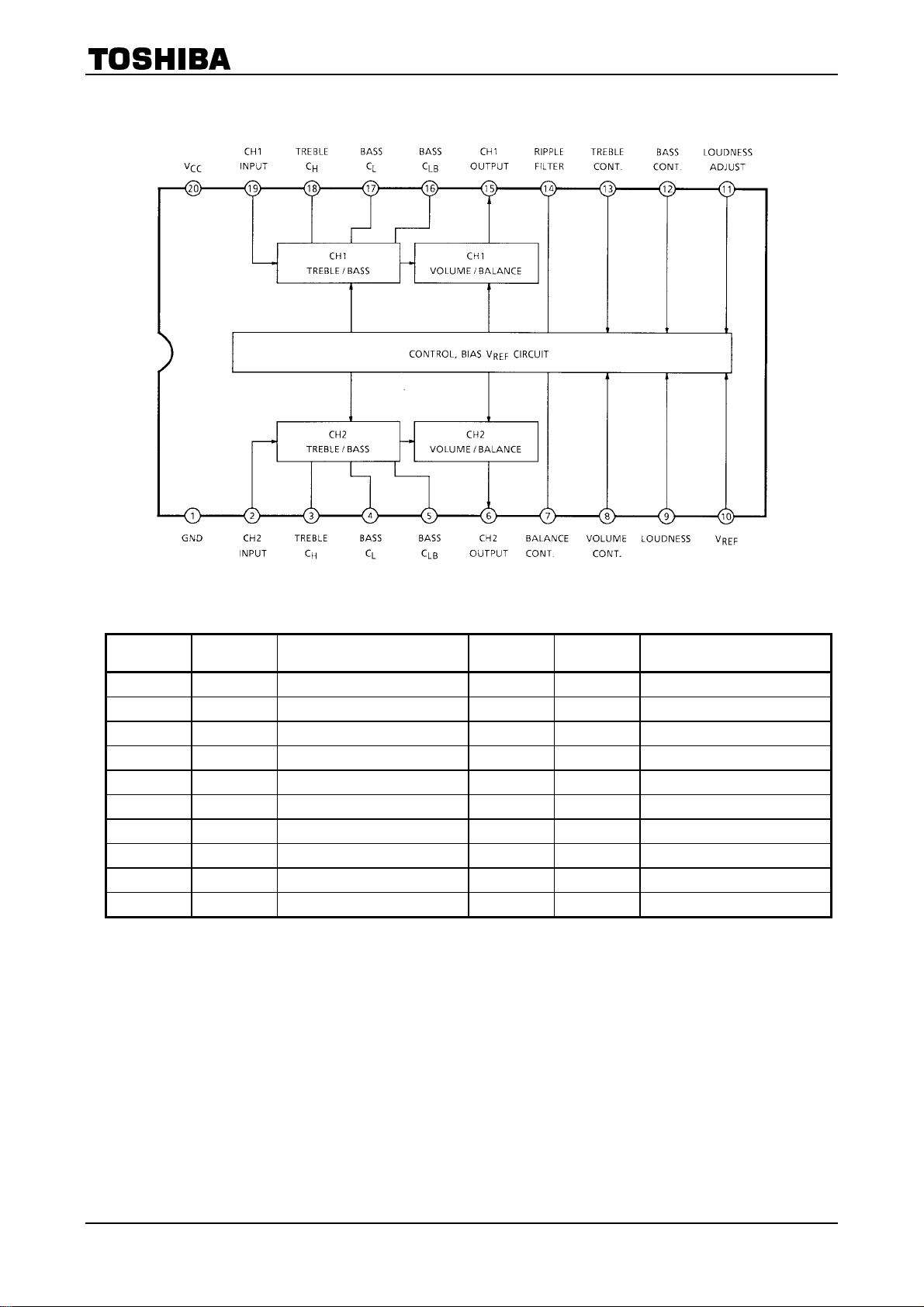
TA8184P/F
Pin Connection
(TA8184F)
Pin Function
Pin No. Symbol Explanation Pin No. Symbol Explanation
1 GND GND 13 L.ADJ. Loudness adjust
2 IN2 CH2, input 14 BASS Bass control
3 N.C 15 N.C
4 C
5 C
6 C
7 OUT2 CH2, output 19 C
8 BAL Balance control 20 C
9 VOL Volume control 21 C
10 N.C 22 N.C
11 LOUD Loudness switch 23 IN1 CH1, input
12 REF Reference 24 V
H (2)
L (2)
LB (2)
CH2, treble control time constant 16 TRBL Treble control
CH2, bass control time constant 17 RIP Ripple filter
CH2, bass control time constant 18 OUT1 CH1, output
LB (1)
L (1)
H (1)
CC
CH1, bass control time constant
CH1, bass control time constant
CH1, treble control time constant
VCC
4
2002-03-05
TA8184P/F
Operating Precautions and Application Methods
(Pin No.: (P/F))
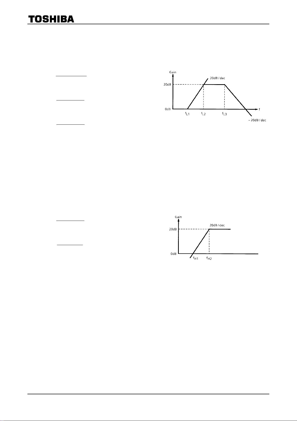
1. How to determine tone controlled frequency characteristic time constants
Bass characteristics determining elements: CL, CLB terminals ((4/5), (5/6), (16/19), (17/20)) Figure 1
Low-bandwidth cut-off frequencies f
equations :
=
f
L1
1
•2
F
C
LB
---(1)
9k10•
(10 kΩ is determined in IC interior)
=
f
L2
1
F
•2
C
LB
----(2)
9k1•
(1 kΩ is determined in IC interior)
=
f
L3
1
F
•2
C
L
----(3)
9k10•
(10 kΩ is determined in IC interior)
Under reference circuits of C
f
≈ 1.59 Hz, fL2 ≈ 15.9 Hz, fL3 ≈ 48.2 Hz
L1
= 0.33 µF and CLB = 10 µF, setting is made as follows:
L
When the characteristics during boosting are considered, crossing with 0dB axis is made at f
starts by 20dB/dec., and flat characteristics of Gain = 20dB is obtained at f
Low-bandwidth f response is determined at f
/dec.
As explained above, low-bandwidth characteristics can be varied by varying C
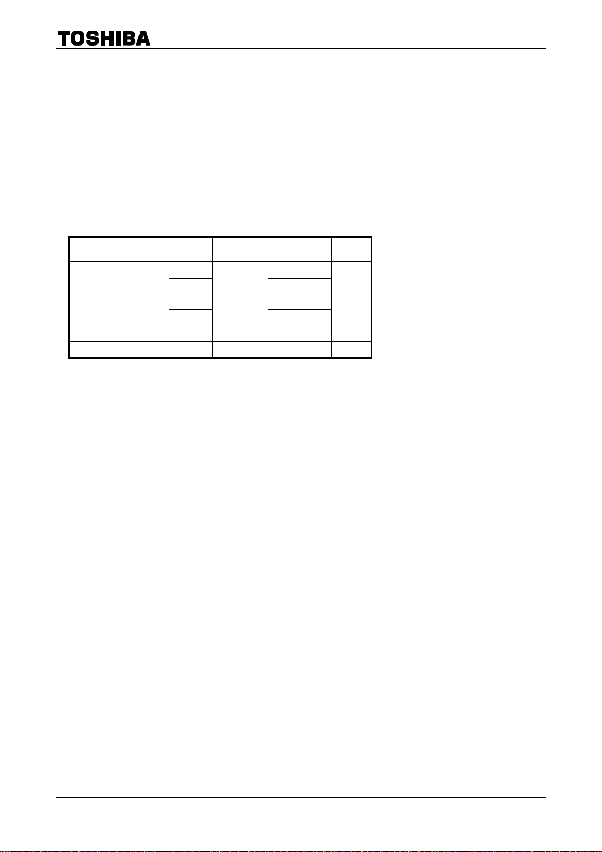
Treble characteristics determining element: CH ((3/4), (18/21))
Figure 2 High-bandwidth cut-off frequencies f
the following equations:
, fL2, fL3 of bass characteristics are determined by the following
L1
Figure 1 Bass characteristics
-namely, CL and gain starts decreasing from fL3 by −20dB
L3
H1
and f
of treble characteristics can be determined by
H2
(during boosting)
.
L2
and CLB.
L
, increase
L1
=
f
H1
1
F
•2
C
H
(10 kΩ is determined in IC interior)
=
f
H2
1
F
•2
C
H
(1 kΩ is determined in IC interior)
Under reference circuit of C
made as follows:
f
≈ 1.94 kHz, fH2 = 19.4 kHz
H1
As explained above, high-bandwidth characteristics can be varied by varying C
By creating the status of C
(f = 100 Hz, 10 kHz) increase but gain near f = 1 kHz is also increased.
On the other hand, when the status of C
near f = 1 kHz approaches 0dB while low/high-bandwidth gains are decreased.
2. Loudness control
By connecting pin (9/11) (loudness terminal) to pin (8/9) (volume terminal), “Loudness” status can be
created. Loudness boost amount is determined by pin (9/11) DC voltage (refer to the subsequently described
G
-V (9/11) data).
V
Loudness is controlled by considering that sound levels will become uniform for all frequency levels
through increasing low/high-bandwidth gains when volume is reduced-namely, sound volume is low.
When loudness control is not used, connect pin (9/11) to pin (10/12) (reference terminal).
The capacitor (typ. 0.047 µF) between pin (9/11) and GND is for reducing pop sound during loudness → ON
while the capacitor (typ. 1 µF) between pin (8/9) and GND is used for the same purpose during loudness →
OFF.
----(4)
9k10•
-----(5)
9k1•
= 0.0082 µF setting is
H
→ decrease and CH → increase, low/high bandwidth gains
L
→ increase and CH → decrease is created, take note that gain
L
Figure 2 Treble characteristics
(during boosting)
.
H
5
2002-03-05
3. Loudness adjustment
When loudness is set, the boost amount can be varied by adjusting voltage at pin (11/13).
Under V (11/13) = 0 V, maximum boost amount is obtained and under V (11/13) = V
(10/12)), minimum boost amount is obtained (refer to the subsequently described G
4. Relations between tone control and loudness
Because of the circuit configuration on this IC, the sum of boost amount by bass/treble control and boost
amount by loudness setting is restricted to become below a constant value. Therefore, the greater the boost
amount in-creases, the lower the boost amount by bass/treble control is reduced because loudness is
extensively applied. As
the subsequent descriptions on tone control frequency response during loudness.)
Maximum Ratings
Characteristics Symbol Rating Unit
opposed to this phenomenon, on the other hand, the cut amount increases. (Refer to
(Ta = 25°C)
TA8184P/F
(connected to pin
REF
− V (11/13) data).
V
Power supply voltage
Power dissipation
Operating temperature T
Storage temperature T
Note 1: Derated above Ta = 25°C in the proportion of 9.6 mW/°C for TA8184P, and of 6.0 mW/°C for TA8184F.
Note 2: Value for mounting on PC board (60 mm × 85 mm × 1.2 mm, Glass epoxy.)
TA8184P 15
TA8184F
TA8184P 1200
TA8184F
VCC
PD (Note 1)
−30~85 °C
opr
−55~150 °C
stg
12.5
750 (Note 2)
V
mW
6
2002-03-05
 Loading...