

Page 1

Colour Television Module
SDI PDP Repair Manual
S37SD-YD02 (37-inch SD v4)
S42SD-YD05, YD06, YD07 (42-inch SD v2, v3, v4)
S42AX-XD02, YD01 (42-inch HD v3, v4)
S50HW-XD03, XD04 (50-inch HD v3, v4)
Contents Page
1. Technical Specifications, Connections, and Chassis
Overview 2
2. Safety Instructions, Warnings, and Notes 15
3. Directions For Use 16
4. Mechanical Instructions 17
5. Service Modes, Error Codes, and Fault Finding 25
6. Block Diagrams, Test Point Overview, and
Waveforms 40
7. Circuit Diagrams and PWB Layouts 51
8. Alignments 52
9. Circuit Descriptions, Abbreviation List, and IC Data
Sheets 71
10. Spare Parts List 72
11. Revision List 77
©
Copyright 2009 Philips Consumer Electronics B.V. Eindhoven, The Netherlands.
All rights reserved. No part of this publication may be reproduced, stored in a
retrieval system or transmitted, in any form or by any means, electronic,
mechanical, photocopying, or otherwise without the prior permission of Philips.
Published by MW 0963 TV Service Printed in the Netherlands Subject to modification EN 3122 785 14994
Page 2
EN 2 SDI PDP1.
Technical Specifications, Connections, and Chassis Overview
1. Technical Specifications, Connections, and Chassis Overview
Index of this chapter:
1.1 PDP Overview
1.2 Serial Numbers
1.3 Chassis Overview
Notes:
• Figures can deviate due to the different model executions.
• Specifications are indicative (subject to change).
1.1 PDP Overview
Table 1-1 PDP overview
PDP Type/Version Model Name H x V Pixel
1 37" SD v4 S37SD-YD02 852 x 480
2 42" SD v2 S42SD-YD06 852 x 480
3 42" SD v3 S42SD-YD05 852 x 480
4 42" SD v4 S42SD-YD07 852 x 480
5 42" HD v3 S42AX-XD02 1024 x 768
6 42" HD v4 S42AX-YD01 1024 x 768
7 50" HD v3 S50HW-XD03 1366 x 768
8 50" HD v4 S50HW-XD04 1366 x 768
Table 1-2 PDP vs Chassis overview
Display type Model # Chassis Chassis Manual #
37" SD v4 37PF9936/37 LC4.7U 3122 785 14742
37" SD v4 37PF9946/12 LC4.7E 3122 785 14722
37" SD v4 37PF9946/69 LC4.7A 3122 785 14761
42" SD v2 420P20/00 FM242 3122 785 14130
42" SD v2 42FD9925/01 FM242 3122 785 14130
42" SD v2 42FD9935/17 FM242 3122 785 14130
42" SD v2 42FD9935/93S FM242 3122 785 14130
42" SD v2 42FD9945/01 FM242 3122 785 14130
42" SD v2 42FD9953/17, /69, /93 FM242 3122 785 14130
42" SD v2 42HF9953/12Z FM24_AB 3122 785 13890
42" SD v2 42PF9936/37 FTP1.1U 3122 785 14381
42" SD v2 42PF9945/12 FTP1.1E 3122 785 14370
42" SD v2 42PF9945/69, /79, /98 FTP1.1U 3122 785 14381
42" SD v2 42PF9955/12 F21RE 3122 785 13890
42" SD v3 42PF9936D/37 LC4.7U 3122 785 14742
42" SD v3 42PF9946/12 LC4.7E 3122 785 14722
42" SD v3 42PF9946/79, /93, /98 LC4.7A 3122 785 14761
42" SD v3 42PF9956/12 FTP2.2E 3122 785 14651
42" SD v3 42PF9956/93 FTP2.2A 3122 785 14680
42" SD v4 42PF7320/10 LC4.9E 3122 785 15431
42" SD v4 42PF7320/79, /98 LC4.9A 3122 785 15450
42" HD v3 42PF9966/37 FTP2.2U 3122 785 14662
42" HD v3 42PF9966/79, /93, /98 FTP2.2A 3122 785 14680
42" HD v3 42PF9976/37 FTP2.2U 3122 785 14662
42" HD v4 42HF7543/37 BP2.3HU 3122 785 15900
42" HD v4 42PF7320A/37 BP2.3U 3122 785 15541
42" HD v4 42PF7520D/10 LC4.9E_AB 3122 785 15670
42" HD v4 42PF9630/78 FTP2.4L 3122 785 15470
42" HD v4 42PF9630A/37 BP2.2U 3122 785 15541
42" HD v4 42PF9630A/96 BP2.2U 3122 785 15541
42" HD v4 42PF9966/79, /98 FTP2.4A 3122 785 15470
50" HD v3 50PF9956/37 FTP2.2U 3122 785 14662
50" HD v3 50PF9966/12 FTP2.2E 3122 785 14651
50" HD v3 50PF9966/37 FTP2.2U 3122 785 14662
50" HD v3 50PF9966/69, /93 FTP2.2A 3122 785 14680
50" HD v4 50HF7543/37 BP2.3HU 3122 785 15900
50" HD v4 50PF7320/10 LC4.9E 3122 785 15431
50" HD v4 50PF7320/79, /93, /98 LC4.9A 3122 785 15450
50" HD v4 50PF9630/78 LC4.9L 3122 785 15450
50" HD v4 50PF9630A/96 BP2.2U 3122 785 15541
50" HD v4 50PF9830A/37 BP2.1U 3122 785 15541
50" HD v4 50PF9966/79 FTP2.4A 3122 785 15470
50" HD v4 50PF9967D/10 FTP2.4E_AB 3122 785 15740
In above table the link is given between the SDI Plasma Display
Panel and the Philips TV chassis (incl. chassis manual no.).
1.1.1 37" SD v4
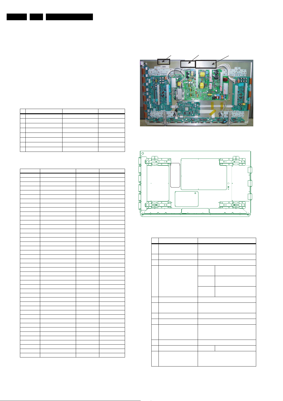
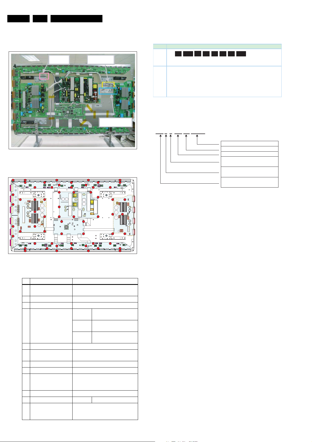
Serial number label
Figure 1-1 External view (37" SD v4)
Figure 1-2 Points of screw mount (37" SD v4)
No Item Specification 37" SD v4
1 Pixel 852 (H) x 480 (V) pixels
2 Number of Cells 2556 (H) x 480 (V)
3 Pixel Pitch 0.960 mm (H) x 0.960 mm (V)
4 Cell Pitch R 0.320 (H) mm
5 Display size 817.92 (H) x 460.80 mm (V)
6 Screen size Diagonal 37" Colour Plasma
7 Screen aspect 16:9
8 Display colour 16.77 million colours
9 Viewing angle Over 160 deg (angle with 50%
10 Dimensions 982 (W) x 582 (H) x 52.9 (D) mm
11 Weight Module 1 About 15.5 kg
12 Broadc. reception
Vertical frequency
Video/Logic Interface
Voltage label Panel module label
F_14991_049.eps
251005
(1 pixel = 1 R,G,B cells)
0.960 (V) mm
G 0.320 (H) mm
0.960 (V) mm
B 0.320 (H) mm
0.960 (V) mm
Display Module
and greater brightness
perpendicular to PDP module)
60/50 Hz, LVDS
Page 3
Technical Specifications, Connections, and Chassis Overview
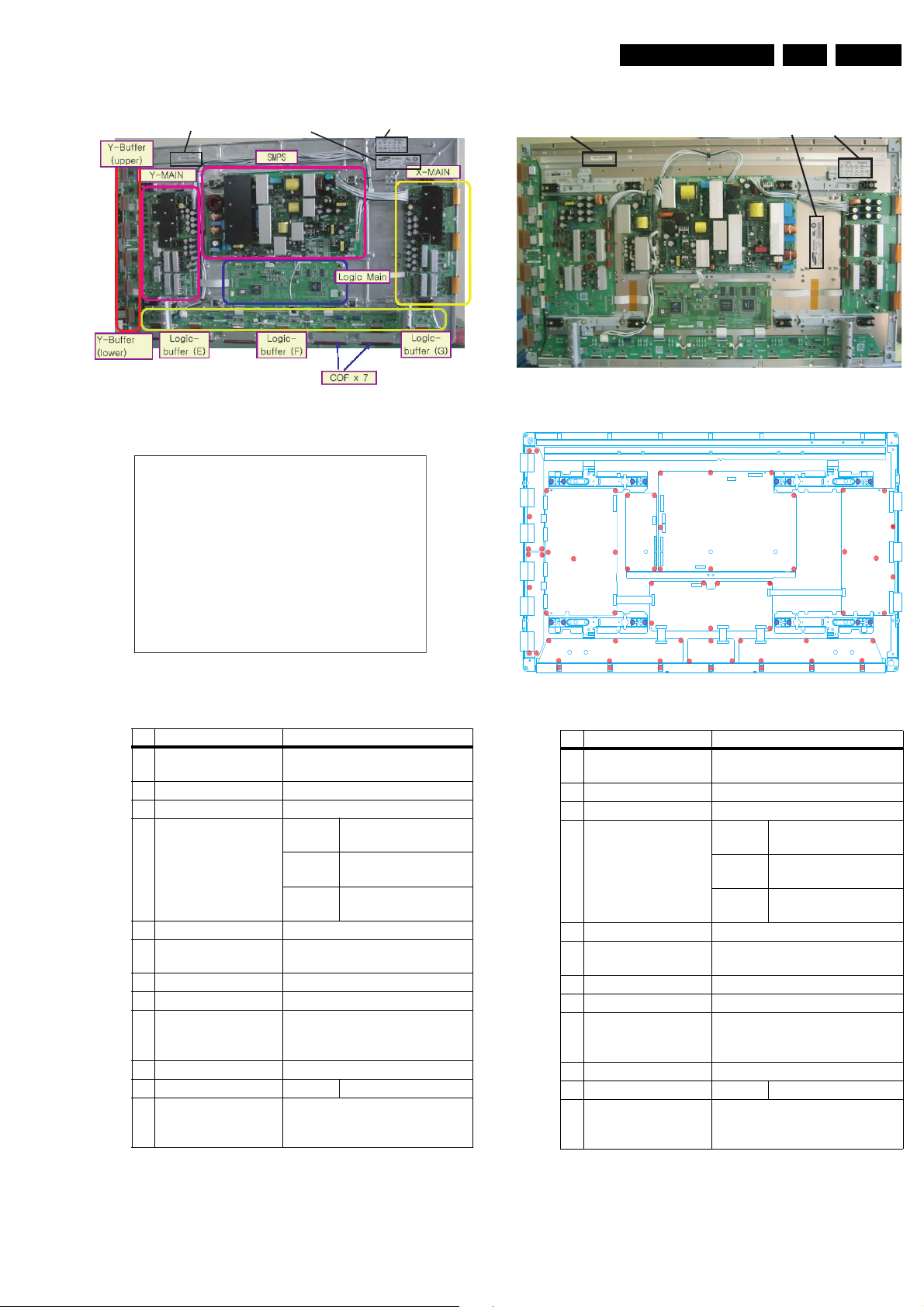
Serial number Model label Voltage label
F_14991_035.eps
061005
This figure is not (yet) available
Serial number label Model label Voltage label
EN 3SDI PDP 1.
1.1.2 42" SD v2
Figure 1-3 External view (42" SD v2)
1.1.3 42" SD v3
Figure 1-5 External view (42" SD v3)
Figure 1-4 Points of screw mount (42" SD v2)
No Item Specification 42" SD v2
1 Pixel 852 (H) x 480 (V) pixels
(1 pixel = 1 R,G,B cells)
2 Number of Cells 2556 (H) x 480 (V)
3 Pixel Pitch 1.095 mm (H) x 1.110 mm (V)
4 Cell Pitch R 0.324 (H) mm
G 0.365 (H) mm
B 0.406 (H) mm
5 Display size 932.940 (H) x 532.800(V) mm
6 Screen size Diagonal 42" Colour Plasma
Display Module
7 Screen aspect 16:9
8 Display colour 16.77 million colours
9 Viewing angle Over 160 deg (angle with 50%
and greater brightness
10 Dimensions 982 (W) x 582 (H) x 52.9 (D) mm
perpendicular to PDP module)
11 Weight Module 1 About 16.6 kg
12 Broadc. reception
60/50 Hz, LVDS
Vertical frequency
Video/Logic Interface
1.110 (V) mm
1.110 (V) mm
1.110 (V) mm
Figure 1-6 Points of screw mount (42" SD v3)
No Item Specification 42" SD v3
1 Pixel 852 (H) x 480 (V) pixels
(1 pixel = 1 R,G,B cells)
2 Number of Cells 2556 (H) x 480 (V)
3 Pixel Pitch 1.095 mm (H) x 1.110 mm (V)
4 Cell Pitch R 0.365 (H) mm
1.110 (V) mm
G 0.365 (H) mm
1.110 (V) mm
B 0.365 (H) mm
1.110 (V) mm
5 Display size 932.940 (H) x 532.800(V) mm
6 Screen size Diagonal 42" Colour Plasma
Display Module
7 Screen aspect 16:9
8 Display colour 16.77 million colours
9 Viewing angle Over 160 deg (angle with 50% and
greater brightness perpendicular
to PDP module)
10 Dimensions 982 (W) x 582 (H) x 52.9 (D) mm
11 Weight Module 1 About 16.6 kg
12 Broadc. reception
60/50 Hz, LVDS
Vertical frequency
Video/Logic Interface
Page 4
EN 4 SDI PDP1.
F_14991_005.eps
180705
Technical Specifications, Connections, and Chassis Overview
1.1.4 42" SD v4
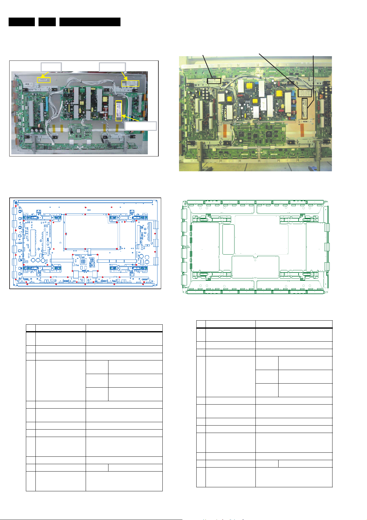
Figure 1-7 External view (42" SD v4)
Serial no.
Voltage label
Panel module label
F_14991_003.eps
1.1.5 42" HD v3
Serial number label Panel model labelVoltage label
180705
Figure 1-9 External view (42" HD v3)
Figure 1-8 Points of screw mount (42" SD v4)
No Item Specification 42" SD v4
1 Pixel 852 (H) x 480 (V) pixels
(1 pixel = 1 R,G,B cells)
2 Number of Cells 2556 (H) x 480 (V)
3 Pixel Pitch 1.095 (H) mm x 1.110 (V) mm
4 Cell Pitch R 0.365 (H) mm x
1.110 (V) mm
G 0.365 (H) mm x
1.110 (V) mm
B 0.365 (H) mm x
1.110 (V) mm
5 Display size 932.940 (H) x 532.800(V) mm
6 Screen size Diagonal 42" Colour Plasma Dis-
play Module
7 Screen aspect 16:9
8 Display colour 16.77 million colours
9 Viewing angle Over 160 deg (angle with 50% and
greater brightness perpendicular
to PDP module)
10 Dimensions 982 (W) x 582 (H) x 54 (D) mm
11 Weight Module 1 About 15.4 kg
14 Broadc. reception
60 Hz/ 50 Hz, LVDS
Vertical frequency
Video/Logic Interface
Figure 1-10 Points of screw mount (42" HD v3)
No Item Specification 42" HD v3
1 Pixel 1.024 (H) x 768 (V) pixels
(1 pixel = 1 R,G,B cells)
2 Number of Cells 3072 (H) x 768 (V)
3 Pixel Pitch 0.912mm (H) x 0.693mm (V)
4 Cell Pitch R Horizontal 0.304 mm
Vertical 0.693 mm
G Horizontal 0.304 mm
Vertical 0.693 mm
B Horizontal 0.304 mm
Vertical 0.693 mm
5 Display size 932.940 (H) x 532.800(V) mm
6 Screen size Diagonal 42" Colour Plasma
Display Module
7 Screen aspect 16:9
8 Display colour 16.77 million colours
9 Viewing angle Over 160 deg (angle with 50% and
greater brightness perpendicular
to PDP module)
10 Dimensions 982 (W) x 582 (H) x 52.9 (D) mm
11 Weight Module 1 About 18.0 kg
12 Broadc. reception
60/50 Hz, LVDS
Vertical frequency
Video/Logic Interface
Page 5
Technical Specifications, Connections, and Chassis Overview
F_14991_010.eps
030805
F_14991_011.eps
030805
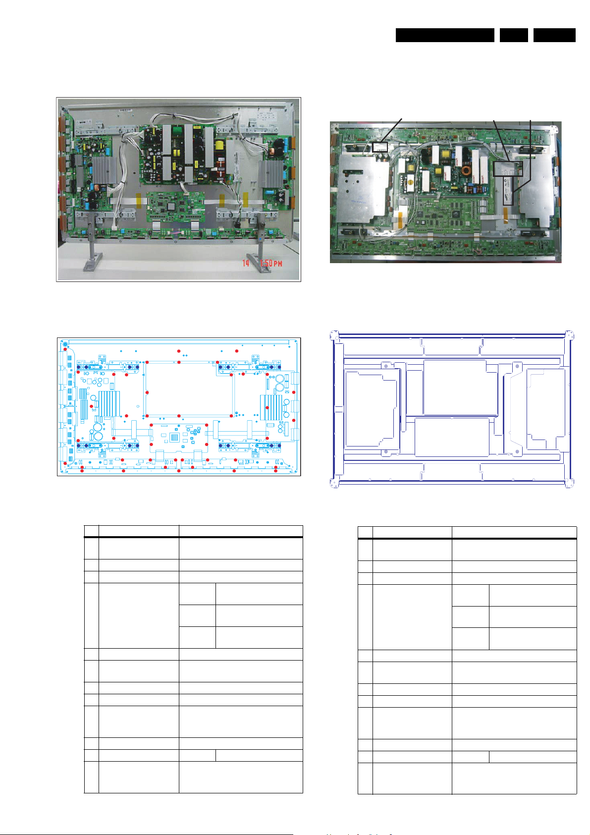
Voltage
label
Serial Number
Panel module label
EN 5SDI PDP 1.
1.1.6 42" HD v4
Figure 1-11 External view (42" HD v4)
1.1.7 50" HD v3
Figure 1-13 External view (50" HD v3)
Figure 1-12 Points of screw mount (42" HD v4)
No Item Specification 42" HD v4
1 Pixel 1.024 (H) x 768 (V) pixels
(1 pixel = 1 R,G,B cells)
2 Number of Cells 3072 (H) x 768 (V)
3 Pixel Pitch 0.912mm (H) x 1.110mm (V)
4 Cell Pitch R Horizontal 0.304 mm
Vertical 0.693 mm
G Horizontal 0.304 mm
Vertical 0.693 mm
B Horizontal 0.304 mm
Vertical 0.693 mm
5 Display size 933.98 (H) x 532.220(V) mm
6 Screen size Diagonal 42" Colour Plasma
7 Screen aspect 16:9
Display Module
8 Display colour 16.77 million colours (8-bit)
9 Viewing angle Over 160 deg (angle with 50% and
greater brightness perpendicular
to PDP module)
10 Dimensions 1000 (W) x 598 (H) x 64.4 (D) mm
11 Weight Module 1 About 20.0 kg
12 Broadc. reception
60/50 Hz, LVDS
Vertical frequency
Video/Logic Interface
Figure 1-14 Points of screw mount (50" HD v3)
No Item Specification 50" HD v3
1 Pixel 1366 (H) x 768 (V) pixels
(1 pixel = 1 R,G,B cells)
2 Number of Cells 4,098 (H) x 768 (V) cells
3 Pixel Pitch 0.810mm (H) mm x 0.810 mm (V)
4 Cell Pitch R Horizontal 0.270mm
Vertical 0.810mm
G Horizontal 0.270mm
Vertical 0.810mm
B Horizontal 0.270mm
Vertical 0.810mm
5 Display size 1106.46 mm (H) x 622.08 mm (H)
6 Screen size Diagonal 50" Colour Plasma
Display Module
7 Screen aspect 16:9
8 Display colour 16.77 million colours
9 Viewing angle Over 160 deg (angle with 50% and
greater brightness perpendicular to
PDP module)
10 Dimensions 1184 (W) x 700 (H) x 60.1 (D) mm
11 Weight Module 1 About 18.0 kg
12 Broadc. reception
60/50 Hz, LVDS
Vertical frequency
Video/Logic Interface
Page 6
EN 6 SDI PDP1.
F_14991_012.eps
030805
Volt age label
Panel module label
Serial No.
F_14991_013.eps
030805
ڞۇڼێێ ڌڏ ڿۄۂۄۏێ
ڤڟ گ۔ۋۀ
ڤڟ
ڨۀڼۉۄۉۂ
ྙ ڜۍۀڼ ڃڞڕ ڞۃۀۊۉڼۉ ڇ ڮ ڕ ڮۃۀۉەۀۉڄ
ྚ ڨۊڿۀۇ ڕ ڎ ڿۄۂۄۏ
ྛ ڨۊڿېۇۀ ڧۄۉۀ ڕ ڜ ۙ ڵ
ྜ ڴۀڼۍ ڕ ڌ ڟۄۂۄۏ ژڙ ڭۊۏڼۏۀ ۀۑۀۍ۔ ڿۀھڼڿۀێ
ྜྷ ڨۊۉۏۃ ڃڣۀۓڕ ڌ ڟۄۂ
ۄۏ ژڙ ڪھۏ ڈ ڜ ڇ کۊۑ ڈ ڝڇ ڟۀھ ڈ ڞڄ
ྞ ڟڼۏۀ ڕ ڌ ۙ ڎڌ
ྟ ڲۊۍۆۀۍ ڢۊېۍۋ ڕ ڜ ګڼۍۏڃڟڼ۔ڄڇ ڝ ګڼۍۏڃڜہۏۀۍۉۊۊۉڄڇ ڞ ګڼۍۏڃکۄۂۃۏڄ
j
h
[ ` W Z WW WX
Area
Mod ule
Line
Ye ar
Month
Da te
S /N
WWX
Mod el
h
Worke r
Gro up
Serial No : 0001~9999
Date : 01~31
Month : 01~12
Year : 00(2000)
~99(2099)
Line No : 1 ~ 9
(0:Pilot Line)
Type : 02~48
(ex.50HDv3:26)
(Step of even)
2 6 1 4 0 8 07 0 8 6 5
Technical Specifications, Connections, and Chassis Overview
1.1.8 50" HD v4
Figure 1-15 External view (50" HD v4)
1.2 Serial Numbers
ڞ
Figure 1-17 Module serial number
F_14991_004.eps
180705
Figure 1-16 Points of screw mount (50" HD v4)
No Item Specification 50" HD v4
1 Pixel 1366 (H) x 768 (V) pixels
2 Number of Cells 4,098 (H) x 768 (V) cells
3 Pixel Pitch 0.810mm (H) mm x 0.810 mm (V)
4 Cell Pitch R Horizontal 0.270mm
5 Display size 1106.46 mm (H) x 622.08 mm (H)
6 Screen size Diagonal 50" Colour Plasma
7 Screen aspect 16:9
8 Display colour 16.77 million colours
9 Viewing angle Over 160 deg (angle with 50% and
10 Dimensions 1175 (W) x 682 (H) x 65.5 (D) mm
11 Weight Module 1 About 25.4 kg
12 Broadc. reception
Vertical frequency
Video/Logic Interface
(1 pixel = 1 R,G,B cells)
Vertical 0.810mm
G Horizontal 0.270mm
Vertical 0.810mm
B Horizontal 0.270mm
Vertical 0.810mm
Display Module
greater brightness perpendicular
to PDP module)
60/50 Hz, LVDS
Figure 1-18 Panel serial number
Page 7
Technical Specifications, Connections, and Chassis Overview
F_14991_027.eps
030805
1
2
3
4
5
6 7 8
12, 13, 14 15, 1610 11
20
17
21
19
18
9
1.3 Chassis Overview
1.3.1 37" SD v4
EN 7SDI PDP 1.
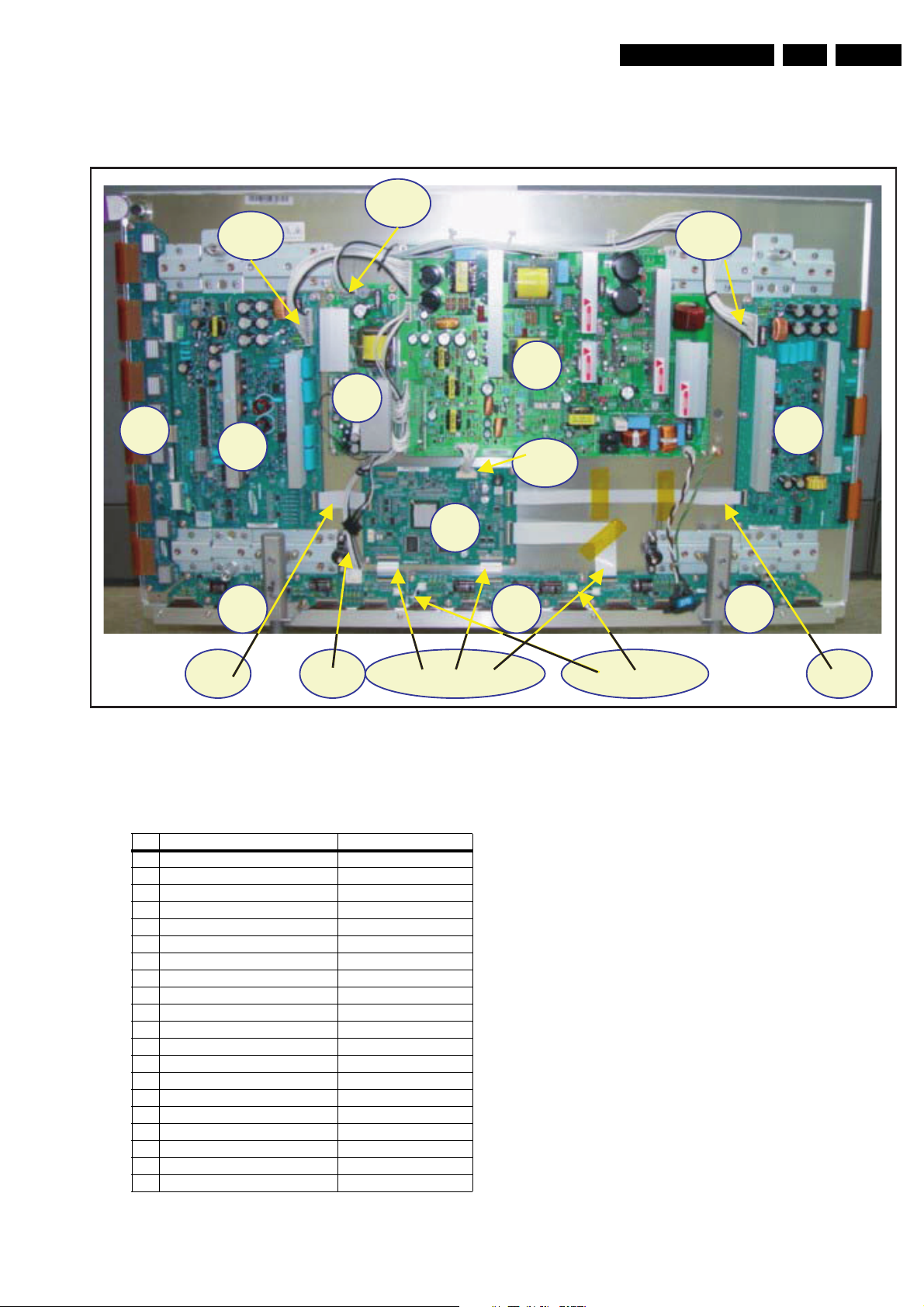
Table 1-3 PWB overview (37" SD v4)
No. Location Name
1 Main PSU Assy PWB PSU
2 SUB-PSU Assy PWB SUB-PSU
3 LOGIC-MAIN Board Assy PWB LOGIC Main
4 X-MAIN Driving Board Assy PWB X Main
5 Y-MAIN Driving Board Assy PWBY Main
6 LOGIC E BUFFER Board Assy PWB Buffer
7 LOGIC F BUFFER Board Assy PWB Buffer
8 LOGIC G BUFFER Board Assy PWB Buffer
9 Y-BUFFER Board Assy PWB Buffer
10 LOGIC + Y-MAIN FFC Cable-flat
11 LOGIC + X-MAIN FFC Cable-flat
12 LOGIC + LOGIC BUF(E) FFC Cable-flat
13 LOGIC + LOGIC BUF(F) FFC Cable-flat
14 LOGIC + LOGIC BUF(G) FFC Cable-flat
15 LOGIC BUF(E) + LOG. BUF(F) Lead connector
16 LOGIC BUF(F) + LOG. BUF(G) Lead connector
17 PSU + SUB PSU Lead connector
18 PSU + LOGIC BUF(E) Lead connector
19 PSU + LOGIC MAIN Lead connector
20 PSU + Y-MAIN Lead connector
Figure 1-19 PWB location (37" SD v4)
Page 8
EN 8 SDI PDP1.
F_14991_033.eps
061005
Logic Ma in
ڮڨګڮ
Y- MAIN
Y- B uffer
(upper)
Y- B uffer
(lower)
X- MAIN
C OF x 7
L
ogic -
buffe r (E )
Logic-
buffe r (F )
Logic
-
buffe r (G )
1.3.2 42" SD v2
Technical Specifications, Connections, and Chassis Overview
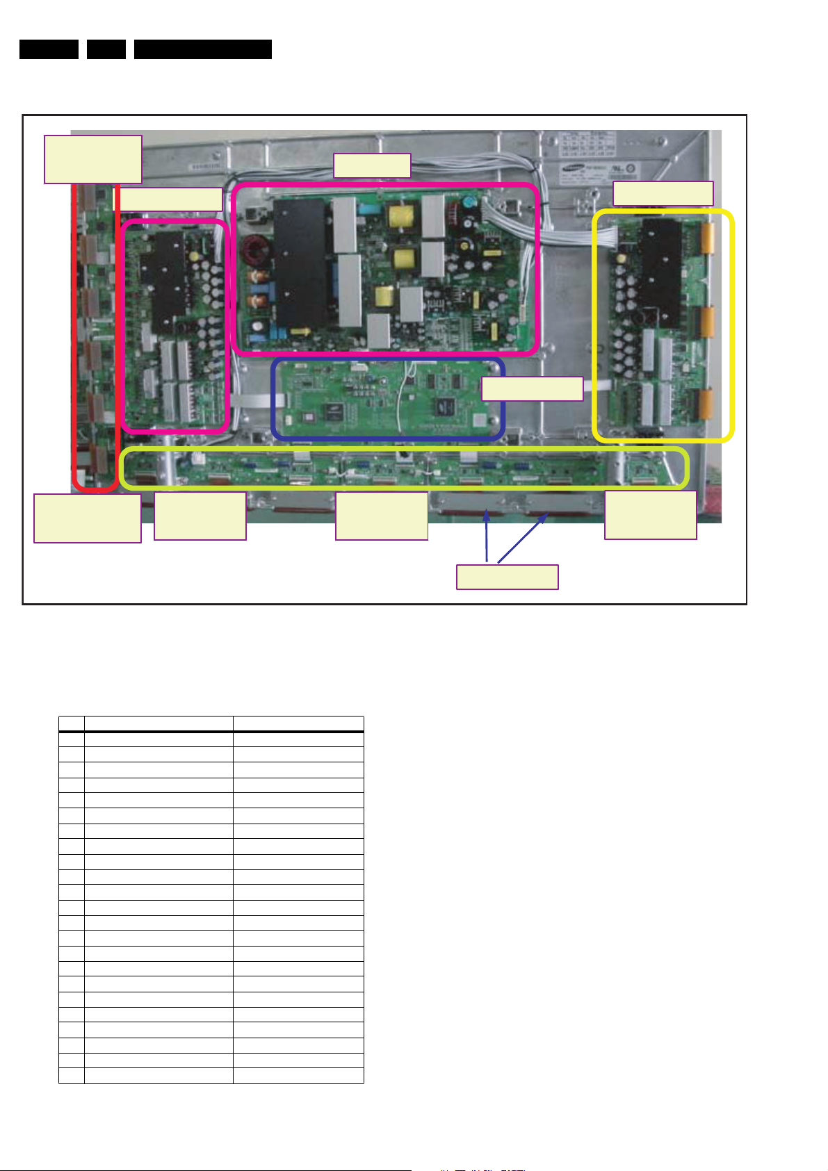
Table 1-4 PWB overview (42" SD v2)
No. Location Name
1 info not available
2
3
4
5
6
7
8
9
10
11
12
13
14
15
16
17
18
19
20
21
22
23
Figure 1-20 PWB location (42" SD v2)
Page 9
1.3.3 42" SD v3
F_14991_034.eps
061005
X_G
YXG YY
X
YG
Z
[G
\G
]G ^ _G
`G
XW
GXZSGX[SGX\ X]SGX^
XX XY
YW
X`G
Technical Specifications, Connections, and Chassis Overview
EN 9SDI PDP 1.
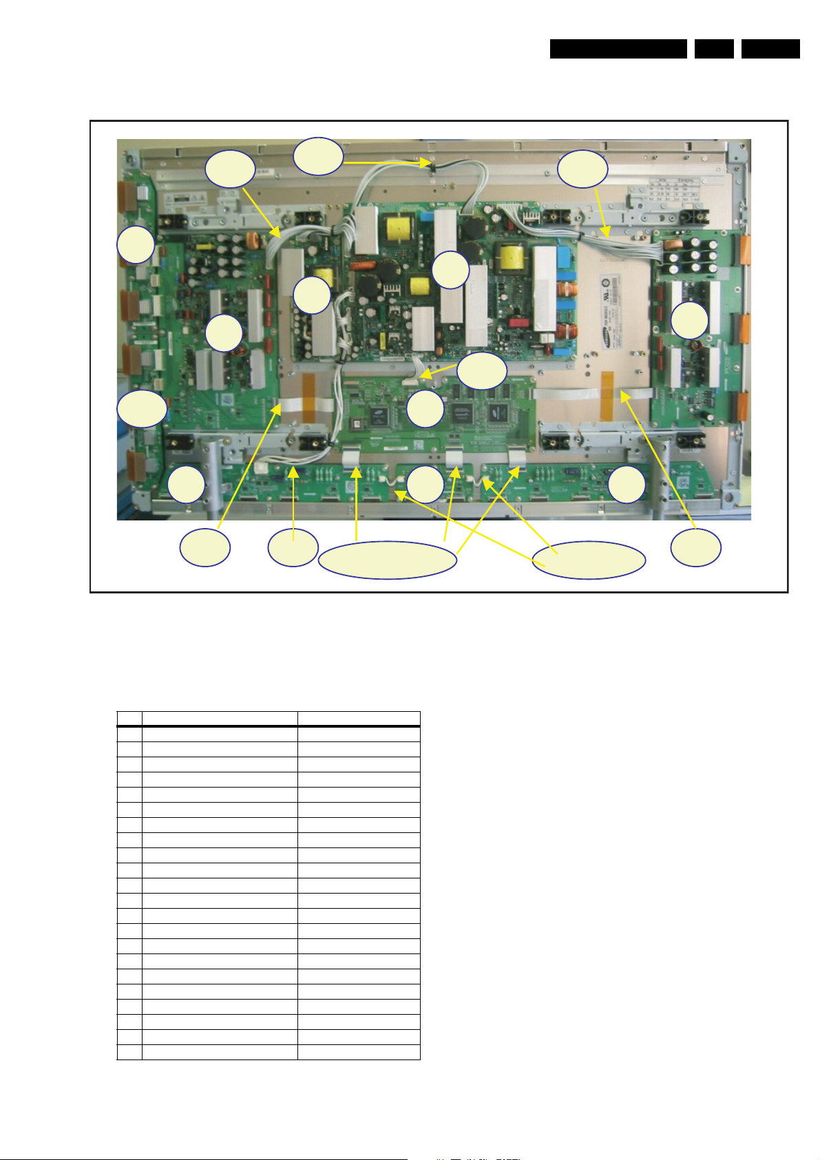
Figure 1-21 PWB location (42" SD v3)
Table 1-5 PWB overview (42" SD v3)
No. Location Name
1 Main PSU Assy PWB PSU
2 SUB-PSU Assy PWB SUB-PSU
3 LOGIC-MAIN Board Assy PWB LOGIC Main
4 X-MAIN Driving Board Assy PWB X Main
5 Y-MAIN Driving Board Assy PWBY Main
6 LOGIC E BUFFER Board Assy PWB Buffer
7 LOGIC F BUFFER Board Assy PWB Buffer
8 LOGIC G BUFFER Board Assy PWB Buffer
9 Y-BUFFER (UPPER) Board Assy PWB Buffer
10 Y-BUFFER (DOWN) Board Assy PWB Buffer
11 LOGIC + Y-MAIN FFC Cable-flat
12 LOGIC + X-MAIN FFC Cable-flat
13 LOGIC + LOGIC BUF(E) FFC Cable-flat
14 LOGIC + LOGIC BUF(F) FFC Cable-flat
15 LOGIC + LOGIC BUF(G) FFC Cable-flat
16 LOGIC BUF(E) +LOG. BUF(F) Lead connector
17 LOGIC BUF(F) +LOG. BUF(G) Lead connector
18 PSU + SUB PSU Lead connector
19 PSU + LOGIC BUF(E) Lead connector
20 PSU + LOGIC MAIN Lead connector
21 PSU + Y-MAIN Lead connector
22 PSU + X-MAIN Lead connector
Page 10
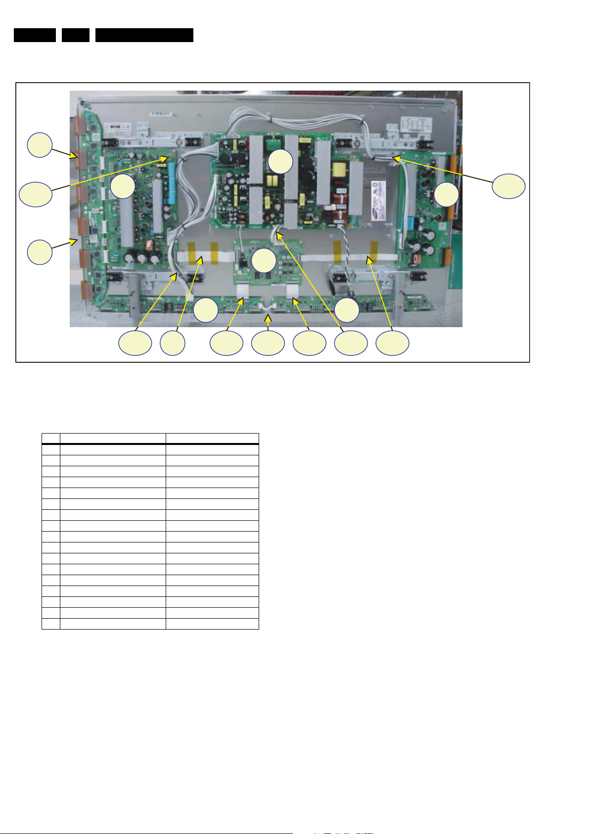
EN 10 SDI PDP1.
1
2
3
174
5 6
7
8
10 9 11 121314
16
15
F_14991_001.eps
180705
1.3.4 42" SD v4
Technical Specifications, Connections, and Chassis Overview
Table 1-6 PWB overview (42" SD v4)
No. Location Name
1 SMPS SMPS
2 LOGIC-MAIN Board Assy PWB Logic Main
3 X-MAIN Driving Board Assy PWB X Main
4 Y-MAIN Driving Board Assy PWB Y Main
5 LOGIC E BUFFER Board Assy PWB buffer
6 LOGIC F BUFFER Board Assy PWB buffer
7 Y-BUFFER (UPPER) Board Assy PWB buffer
8 Y-BUFFER (DOWN) Board Assy PWB buffer
9 LOGIC + Y-MAIN FFC cable-flat
10 LOGIC + X-MAIN FFC cable-flat
11 LOGIC + LOGIC BUF (E) FFC cable-flat
12 LOGIC + LOGIC BUF (F) FFC cable-flat
13 LOGIC BUF (E) + (F) Lead connector
14 SMPS + LOGIC BUF (E) Lead connector
15 SMPS + LOGIC MAIN Lead connector
16 SMPS + Y-MAIN Lead connector
17 SMPS + X-MAIN Lead connector
Figure 1-22 PWB location (42" SD v4)
Page 11
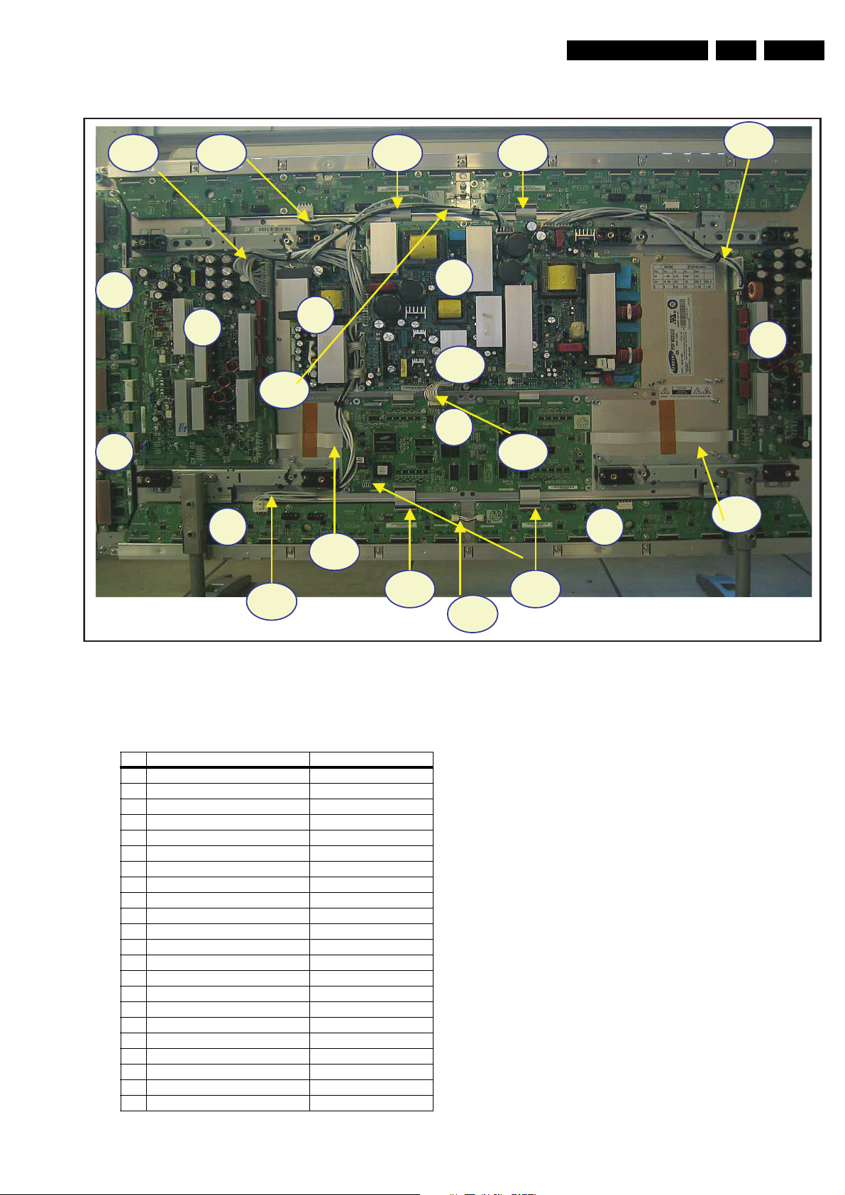
1.3.5 42" HD v3
Technical Specifications, Connections, and Chassis Overview
EN 11SDI PDP 1.
8
9
5
18 21
14 15
1
2
4
20
17
3
20
11
22
6
7
10
19
13
Figure 1-23 PWB location (42" HD v3)
Table 1-7 PWB overview (42" HD v3)
No. Location Name
1 Main PSU Assy PWB PSU
2 SUB-PSU Assy PWB SUB-PSU
3 LOGIC-MAIN Board Assy PWB LOGIC Main
4 X-MAIN Driving Board Assy PWB X Main
5 Y-MAIN Driving Board Assy PWB Y Main
6 LOGIC E BUFFER Board Assy PWB Buffer
7 LOGIC F BUFFER Board Assy PWB Buffer
8 Y-BUFFER (UPPER) Board Assy PWB BuffeR
9 Y-BUFFER (DOWN) Board Assy PWB Buffer
10 LOGIC + Y-MAIN FFC Cable-flat
11 LOGIC + X-MAIN FFC Cable-flat
12 LOGIC + LOG. BUF(E) (Down) FFC Cable-flat
13 LOGIC + LOG. BUF(F) (Down) FFC Cable-flat
14 LOGIC + LOGIC BUF(E) (Up) FFC Cable-flat
15 LOGIC + LOGIC BUF(E) (Up) FFC Cable-flat
16 LOGIC BUF(E) + LOG. BUF(F) Lead connector
17 PSU + SUB PSU Lead connector
18 PSU + LOGIC BUF(E) (UP) Lead connector
19 PSU + LOGIC BUF(E) (Down) Lead connector
20 PSU + LOGIC MAIN Lead connector
21 PSU + Y-MAIN Lead connector
22 PSU + X-MAIN Lead connector
12
16
F_14991_014.eps
030805
Page 12
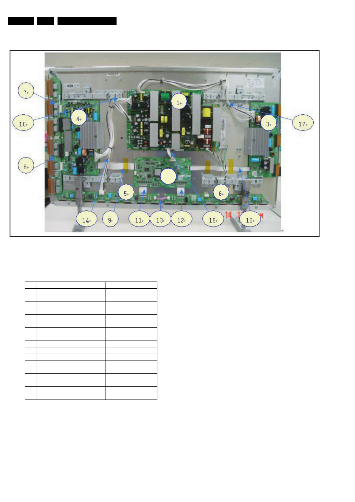
EN 12 SDI PDP1.
F_14991_015.eps
030805
Y
1.3.6 42" HD v4
Technical Specifications, Connections, and Chassis Overview
Figure 1-24 PWB location (42" HD v4)
Table 1-8 PWB overview (42" HD v4)
No. Location Name
1 SMPS SMPS
2 LOGIC-MAIN Board Assy PWBLOGIC Main
3 X-MAIN Driving Board Assy PWBX Main
4 Y-MAIN Driving Board Assy PCBY Main
5 LOGIC E BUFFER Board Assy PWB Buffer
6 LOGIC F BUFFER Board Assy PWB Buffer
7 Y-BUFFER (UPPER) Board Assy PWB Buffer
8 Y-BUFFER (DOWN) Board Assy PWB Buffer
9 LOGIC + Y-MAIN FFC Cable-flat
10 LOGIC + X-MAIN FFC Cable-flat
11 LOGIC + LOGIC BUF(E) FFC Cable-flat
12 LOGIC + LOGIC BUF(F) FFC Cable-flat
13 LOGIC BUF(E) + LOG. BUF(F) Lead connector
14 SMPS + LOGIC BUF(E) Lead connector
15 SMPS + LOGIC MAIN Lead connector
16 SMPS + Y-MAIN Lead connector
17 SMPS + X-MAIN Lead connector
Page 13
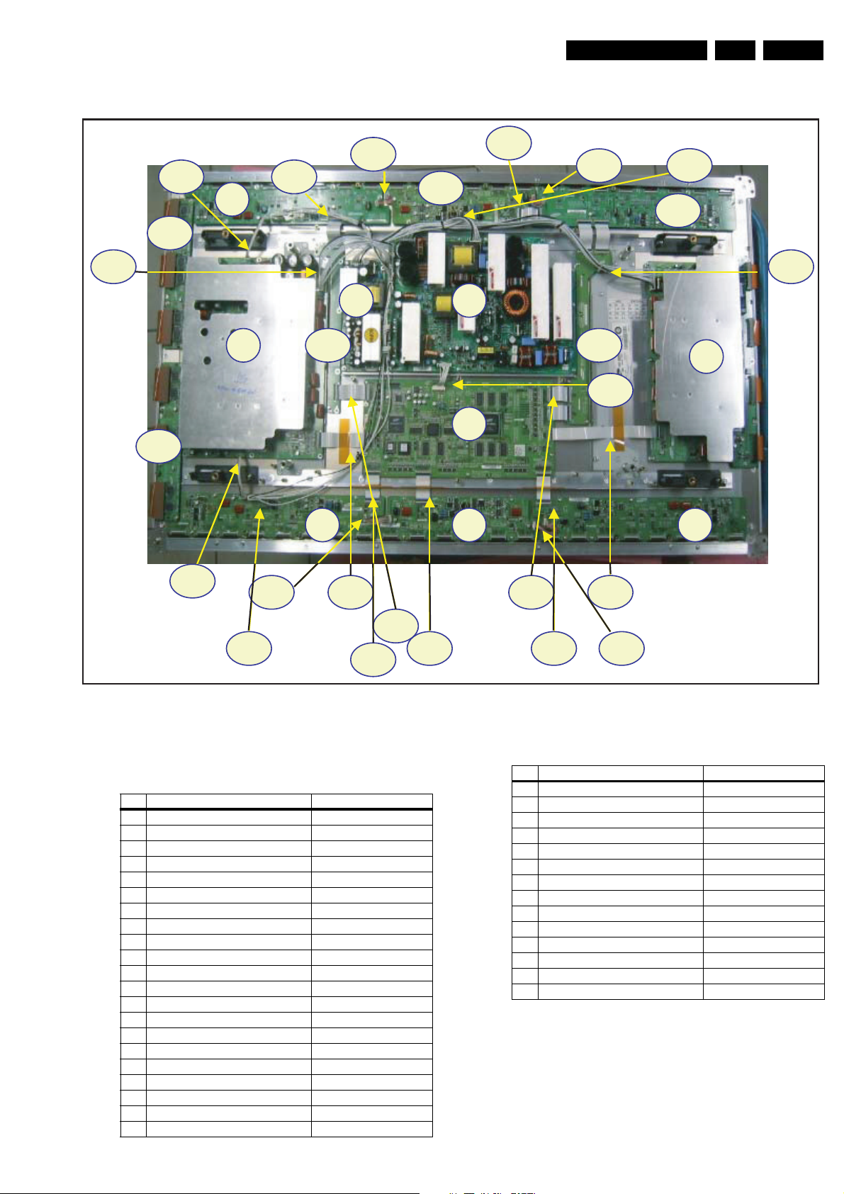
1.3.7 50" HD v3
F_14991_016.eps
030805
20
26
35
27
28 32
10
9
11
12
33 34
2 1
5 14 15
4
30
3
13
6 7 8
24
21
22
19
16
18 17
29
31 23 25
Technical Specifications, Connections, and Chassis Overview
EN 13SDI PDP 1.
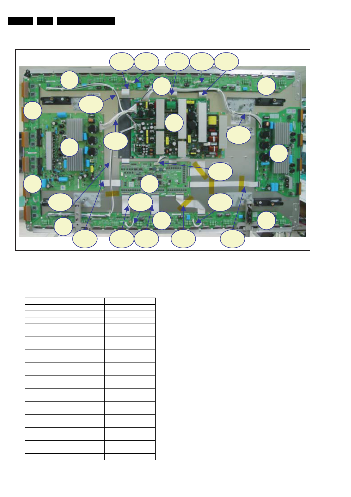
Table 1-9 PWB overview (50" HD v3)
No. Location Name
1 Main PUS Assy PWBPSU
2 SUB-PSU Assy PWBSUB-PSU
3 LOGIC-MAIN Board Assy PWBLOGIC Main
4 X-MAIN Driving Board Assy PWBX Main
5 Y-MAIN Driving Board Assy PCBY Main
6 LOGIC E BUFFER Board Assy PWB Buffer
7 LOGIC F BUFFER Board Assy PWB Buffer
8 LOGIC G BUFFER Board Assy PWB Buffer
9 LOGIC H BUFFER Board Assy PWB Buffer
10 LOGIC I BUFFER Board Assy PWB Buffer
11 LOGIC J BUFFER Board Assy PWB Buffer
12 Y-BUFFER (UPPER) Board Assy PWB Buffer
13 Y-BUFFER (DOWN) Board Assy PWB Buffer
14 SUB-R Assy PWB Buffer
15 SUB-L Assy PWB Buffer
16 LOGIC + Y-MAIN FFC Cable-flat
17 LOGIC + X-MAIN FFC Cable-flat
18 SUB R + LOGIC FFC Cable-flat
19 SUB L + LOGIC FFC Cable-flat
20 LOG.BUF(I) + LOG.BUF(J) (Up) FFC Cable-flat
21 LOGIC + LOG. BUF(E) (Down) FFC Cable-flat
Figure 1-25 PWB location (50" HD v3)
No. Location Name
22 LOGIC + LOG. BUF(F) (Down) FFC Cable-flat
23 LOGIC + LOG. BUF(G) (Down) FFC Cable-flat
24 LOGIC BUF(E) + LOG. BUF(F) Lead connector
25 LOGIC BUF(F) + LOG. BUF(G) Lead connector
26 LOGIC BUF(H) + LOG. BUF(I) Lead connector
27 LOGIC BUF(I) + LOG. BUF(J) Lead connector
28 Y-MAIN + LOGIC BUF(H) Lead connector
29 Y-MAIN + LOGIC BUF(E) Lead connector
30 PSU + LOGIC MAIN Lead connector
31 PSU + LOGIC BUF(E) Lead connector
32 PSU + LOGIC BUF(H) Lead connector
33 PSU + Y-MAIN Lead connector
34 PSU + X-MAIN Lead connector
35 PSU + SUB PSU Lead connector
Page 14
EN 14 SDI PDP1.
F_14991_017.eps
030805
1
2
4
6
7
11
10 12 14
15 16
18
5
6
17
19
22
23
24
1918
21
20
13
7
8
3
9
5
1.3.8 50" HD v4
Technical Specifications, Connections, and Chassis Overview
Figure 1-26 PWB location (50" HD v4)
Table 1-10 PWB overview (50" HD v4)
No. Location Name
1 SMPS SMPS
2 LOGIC-MAIN Board Assy PWBLOGIC Main
3 X-MAIN Driving Board Assy PWBX Main
4 Y-MAIN Driving Board Assy PCBY Main
5 LOGIC E BUFFER Board Assy PWB Buffer
6 LOGIC F BUFFER Board Assy PWB Buffer
7 LOGIC G BUFFER Board Assy PWB Buffer
8 Y-BUFFER (Upper) Board Assy PWB Buffer
9 Y-BUFFER (Down) Board Assy PWB Buffer
10 LOGIC + Y-MAIN FFC Cable-flat
11 LOGIC + X-MAIN FFC Cable-flat
12 LOGIC + LOG. BUF(G: Down) FFC Cable-flat
13 LOGIC + LOG. BUF(F: Down) FFC Cable-flat
14 LOGIC + LOG. BUF(E: Down) FFC Cable-flat
15 LOGIC + LOG. BUF(E: Upper) FFC Cable-flat
16 LOGIC + LOG. BUF(F: Upper) FFC Cable-flat
17 LOGIC + LOG. BUF(G: Upper) FFC Cable-flat
18 LOGIC BUF(E) + LOG. BUF(F) Lead connector
19 LOGIC BUF(F) + LOG. BUF(G) Lead connector
20 SMPS + LOGIC BUF(G: Down) Lead connector
21 SMPS + LOGIC BUF(E: Upper) Lead connector
22 SMPS + LOGIC MAIN Lead connector
23 SMPS + Y-MAIN Lead connector
24 SMPS + X-MAIN Lead connector
Page 15

Safety Instructions, Warnings, and Notes
2. Safety Instructions, Warnings, and Notes
EN 15SDI PDP 2.
Index of this chapter:
2.1 Handling Precautions
2.2 Safety Precautions
2.3 Notes
Notes:
• Only authorised persons should perform servicing of this
module.
• When using/handling this unit, pay special attention to the
PDP Module: it should not be enforced into any other way
then next rules, warnings, and/or cautions.
• “Warning” indicates a hazard that may lead to death or
injury if the warning is ignored and the product is handled
incorrectly.
• “Caution” indicates a hazard that can lead to injury or
damage to property if the caution is ignored and the
product is handled incorrectly.
2.1 Handling Precautions
• The PDP module use high voltage that is dangerous to
humans. Before operating the PDP, always check for dust
to prevent short circuits. Be careful touching the circuit
device when power is “on”.
• The PDP module is sensitive to dust and humidity.
Therefore, assembling and disassembling must be done in
no dust place.
• The PDP module has a lot of electric devices. The service
engineer must wear equipment (for example, earth ring) to
prevent electric shock and working clothes to prevent
electrostatic.
• The PDP module use a fine pitch connector which is only
working by exactly connecting with flat cable. The operator
must pay attention to a complete connection when
connector is reconnected after repairing.
• The capacitor’s remaining voltage in the PDP module’s
circuit board temporarily remains after power is “off”.
Operator must wait for discharging of remaining voltage
during at least 1 minute.
2.2 Safety Precautions
2.2.1 Safety Precautions
parts and circuit board. Check the cord of AC power
preparing damage.
• Product Safety Mark: Some of electric or implement
material have special characteristics invisible that was
related on safety. In case of the parts are changed with new
one, even though the Voltage and Watt is higher than
before, the Safety and Protection function will be lost.
• The AC power always should be turned “off”, before next
repair.
• Check assembly condition of screw, parts and wire
arrangement after repairing. Check whether the material
around the parts get damaged.
2.2.2 ESD Precautions
There are parts, which are easily damaged by electrostatics
(for example Integrated Circuits, FETs, etc.) Electrostatic
damage rate of product will be reduced by the following
technics:
• Before handling semiconductor parts/assembly, must
remove positive electric by ground connection, or must
wear the antistatic wrist-belt and ring (it must be operated
after removing dust on it. It comes under precaution of
electric shock).
• After removing the assembly, lay it with the tracks on a
conductive surface to prevent charging.
• Do not use chemical stuff containing Freon. It generates
positive electric that can damage ESD sensitive devices.
• You must use a soldering device for ground-tip when
soldering or de-soldering these devices.
• You must use anti-static solder removal device. Most
removal devices do not have antistatic which can charge a
enough positive electric enough for damaging these
devices.
• Before removing the protective material from the lead of a
new device, bring the protective material into contact with
the chassis or assembly.
• When handing an unpacked device for replacement, do not
move around too much. Moving (legs on the carpet, for
example) generates enough electrostatic to damage the
device.
• Do not take a new device from the protective case until the
it is ready to be installed. Most devices have a lead, which
is easily short-circuited by conductive materials (such as
conductive foam and aluminium)
• Before replacing a board, discharge forcibly.
• The remaining electricity from board.
• When connecting FFC and TCPs to the module, recheck
that they are perfectly connected.
• To prevent electrical shock, be careful not to touch leads
during circuit operations.
• To prevent the Logic circuit from being damaged due to
wrong working, do not connect/disconnect signal cables
during circuit operations.
• Do thoroughly adjustment of a voltage label and voltageinsulation.
• Before reinstalling the chassis and the chassis assembly,
be sure to use all protective stuff including a nonmetal
controlling handle and the covering of partitioning type.
• Caution for design change: Do not install any additional
devices to the module, and do not change the electrical
circuit design.
• For example: Do not insert a subsidiary audio or video
connector. If you insert It, it cause danger on safety. And, if
you change the design or insert, manufacturer guarantee
will be not effect.
• If any parts of wire is overheats of damaged, replace it with
a new specified one immediately, and identify the cause of
the problem and remove the possible dangerous factors.
• Examine carefully the cable status if it is twisted or
damaged or displaced. Do not change the space between
2.3 Notes
A glass plate is positioned before the plasma display. This
glass plate can be cleaned with a slightly humid cloth. If due to
circumstances there is some dirt between the glass plate and
the plasma display panel, it is recommended to do some
maintenance by a qualified service employee only.
2.3.1 Safe PDP Handling
• The work procedures shown with the “Note” indication are
important for ensuring the safety of the product and the
servicing work. Be sure to follow these instructions.
• Before starting the work, secure a sufficient working space.
• At all times, other than when adjusting and checking the
product, be sure to turn “off” the main POWER switch and
disconnect the power cable from the power source of the
display (jig or the display itself) during servicing.
• To prevent electric shock and breakage of PWBs, start the
servicing work at least 30 seconds after the main power
has been turned “off”. Especially when installing and
removing the Power Supply PWB and the SUS PWB in
which high voltages are applied, start servicing at least 2
minutes after the main power has been turned “off”.
Page 16

EN 16 SDI PDP3.
Directions For Use
• While the main power is “on”, do not touch any parts or
circuits other than the ones specified. The high voltage
Power Supply block within the PDP module has a floating
ground. If any connection other than the one specified is
made between the measuring equipment and the high
voltage power supply block, it can result in electric shock or
activation of the leakage-detection circuit breaker.
• When installing the PDP module in, and removing it from
the packing carton, be sure to have at least two persons
perform the work while being careful to ensure that the
flexible printed-circuit cable of the PDP module does not
get caught by the packing carton.
• When the surface of the panel comes into contact with the
cushioning materials, be sure to confirm that there is no
foreign matter on top of the cushioning materials before the
surface of the panel comes into contact with the cushioning
materials. Failure to observe this precaution may result in,
the surface of the panel being scratched by foreign matter.
• When handling the circuit PWB, be sure to remove static
electricity from your body before handling the circuit PWB.
• Be sure to handle the circuit PWB by holding the large parts
as the heat sink or transformer. Failure to observe this
3. Directions For Use
Not applicable.
precaution may result in the occurrence of an abnormality
in the soldered areas.
• Do not stack the circuit PWB. Failure to observe this
precaution may result in problems resulting from scratches
on the parts, the deformation of parts, and short-circuits
due to residual electric charge.
• Routing of the wires and fixing them in position must be
done in accordance with the original routing and fixing
configuration when servicing is completed. All the wires are
routed far away from the areas that become hot (such as
the heat sink). These wires are fixed in position with the
wire clamps so that the wires do not move, thereby
ensuring that they are not damaged and their materials do
not deteriorate over long periods of time. Therefore, route
the cables and fix the cables to the original position and
states using the wire clamps.
• Perform a safety check when servicing is completed. Verify
that the peripherals of the serviced points have not
undergone any deterioration during servicing. Also verify
that the screws, parts and cables removed for servicing
purposes have all been returned to their proper locations in
accordance with the original
Page 17
4. Mechanical Instructions
Index of this chapter:
4.1 Dis-assembling / Re-assembling
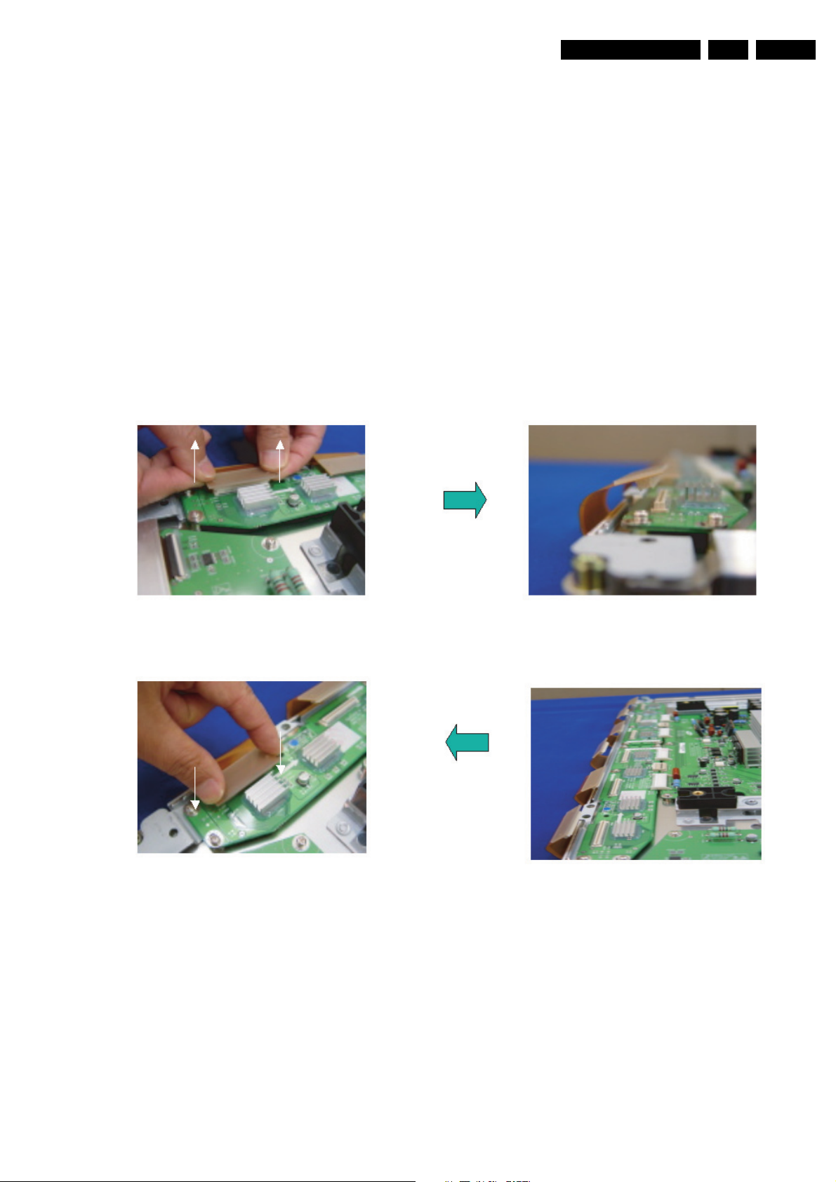
4.1.1 Flexible Printed Circuit of Y-Buffer (Upper and Lower)
4.1.2 Flat Cable Connector of X-main Board
4.1.3 FFC and TCP from Connector
4.1.4 Exchange of LBE, LBF, LBG board
4.1.5 Exchange YBU, YBL and YM board
4.1 Dis-assembling / Re-assembling
4.1.1 Flexible Printed Circuit of Y-Buffer (Upper and Lower)
• Dis-assembly: Pull out the FPC from the connector by
holding the lead of the FPC with both hands.
• Re-assembly: Push the lead of FPC with same force on
both sides into the connector.
Note: Be careful do not to damage the connector pin
during connecting.
Mechanical Instructions
EN 17SDI PDP 4.
Figure 4-1 Dis-assembly FPC of Y-buffer
Figure 4-2 Re-assembly FPC of Y-buffer
Page 18
EN 18 SDI PDP4.
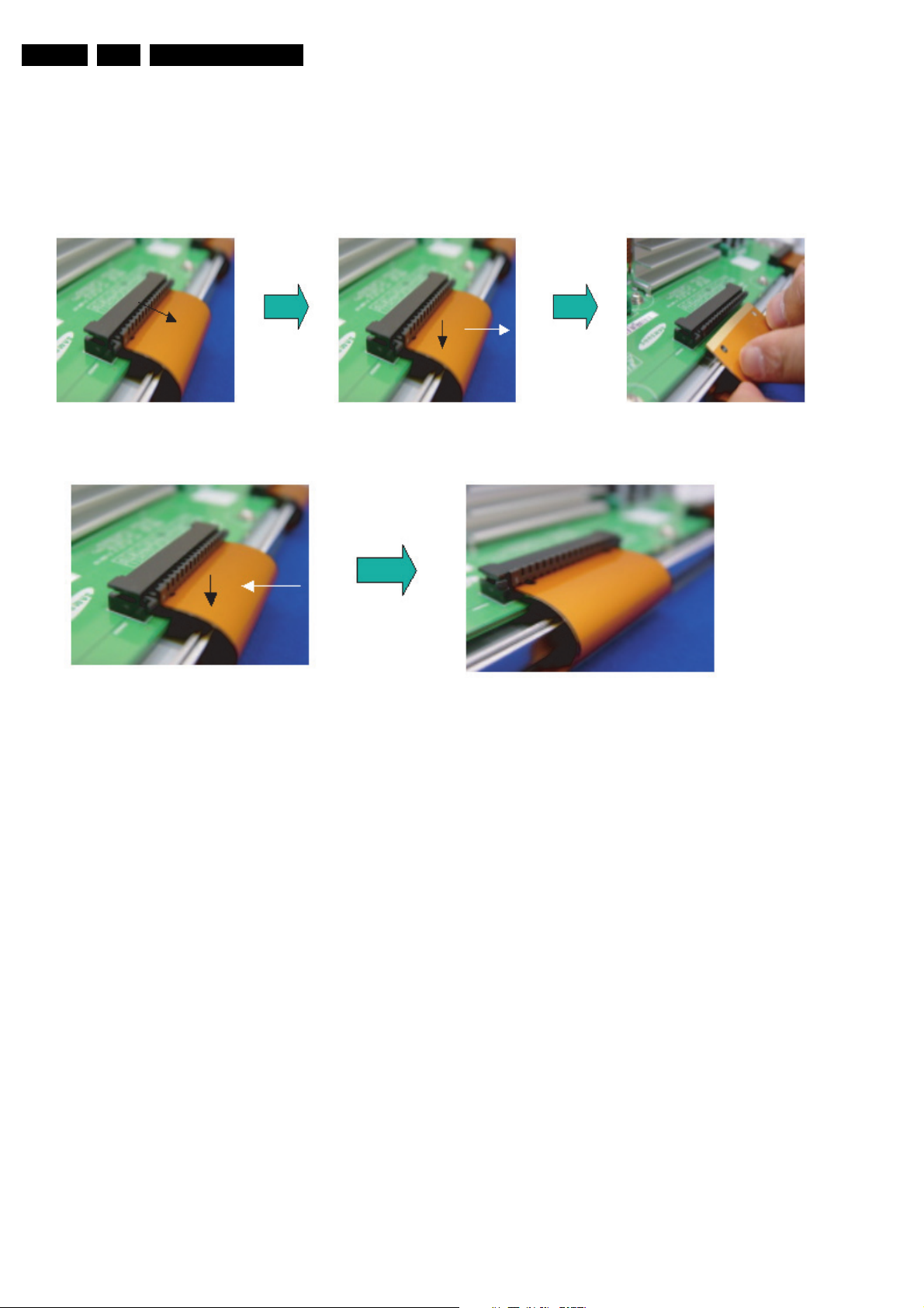
4.1.2 Flat Cable Connector of X-main Board
• Dis-assembly:
1. Pull out the clamp of connector.
2. Pull Flat cable out press down lightly.
3. Turn the Flat Cable reversely.
• Re-assembly: Put the Flat Cable into the connector press
down lightly until locking sound (“Click“) comes out.
Figure 4-3 Dis-assembly FCC of X-main board
Mechanical Instructions
Figure 4-4 Re-assembly FCC of X-main board
Page 19
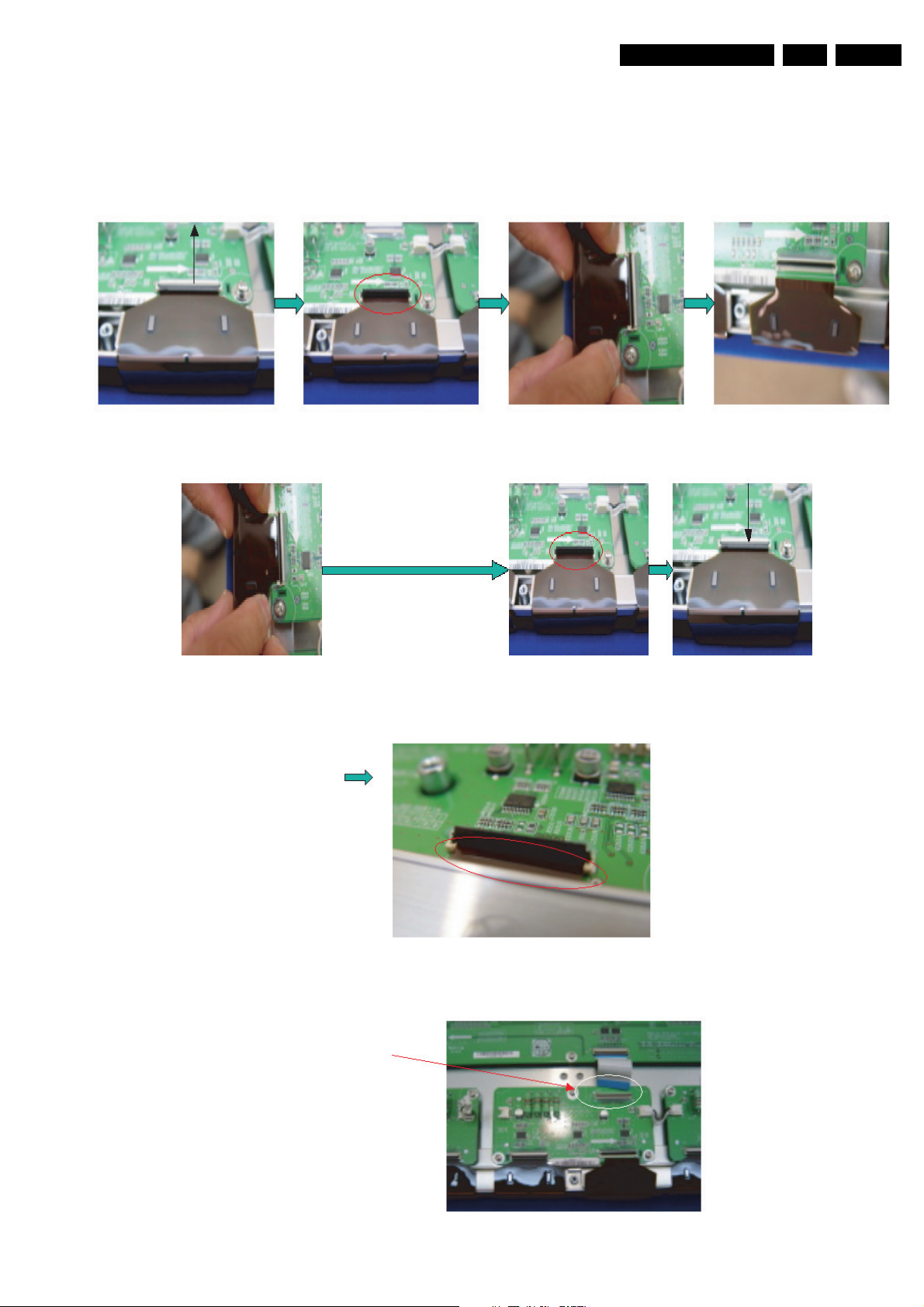
4.1.3 FFC and TCP from Connector
The procedure of
assembling and disassembling of
FFC is same as TCP
• Dis-assembling of TCP:
1. Open the clamp carefully.
2. Pull the TCP out from its connector.
• Re-assembling of TCP:
1. Put the TCP into the connector carefully
2. Close the clamp completely (until “Click” comes out.).
Mechanical Instructions
Notes:
• Checking whether the foreign material is on the connector
• Be careful, do not damage the board by ESD during
Figure 4-5 Dis-assembly of TCP
EN 19SDI PDP 4.
inside before assembling of TCP.
handling of TCP.
Figure 4-6 Re-assembly of TCP
Figure 4-7 Mis-assembly of TCP
Figure 4-8 Dis- and re-assembly of FFC
Page 20
EN 20 SDI PDP4.
4.1.4 Exchange of LBE, LBF, LBG board
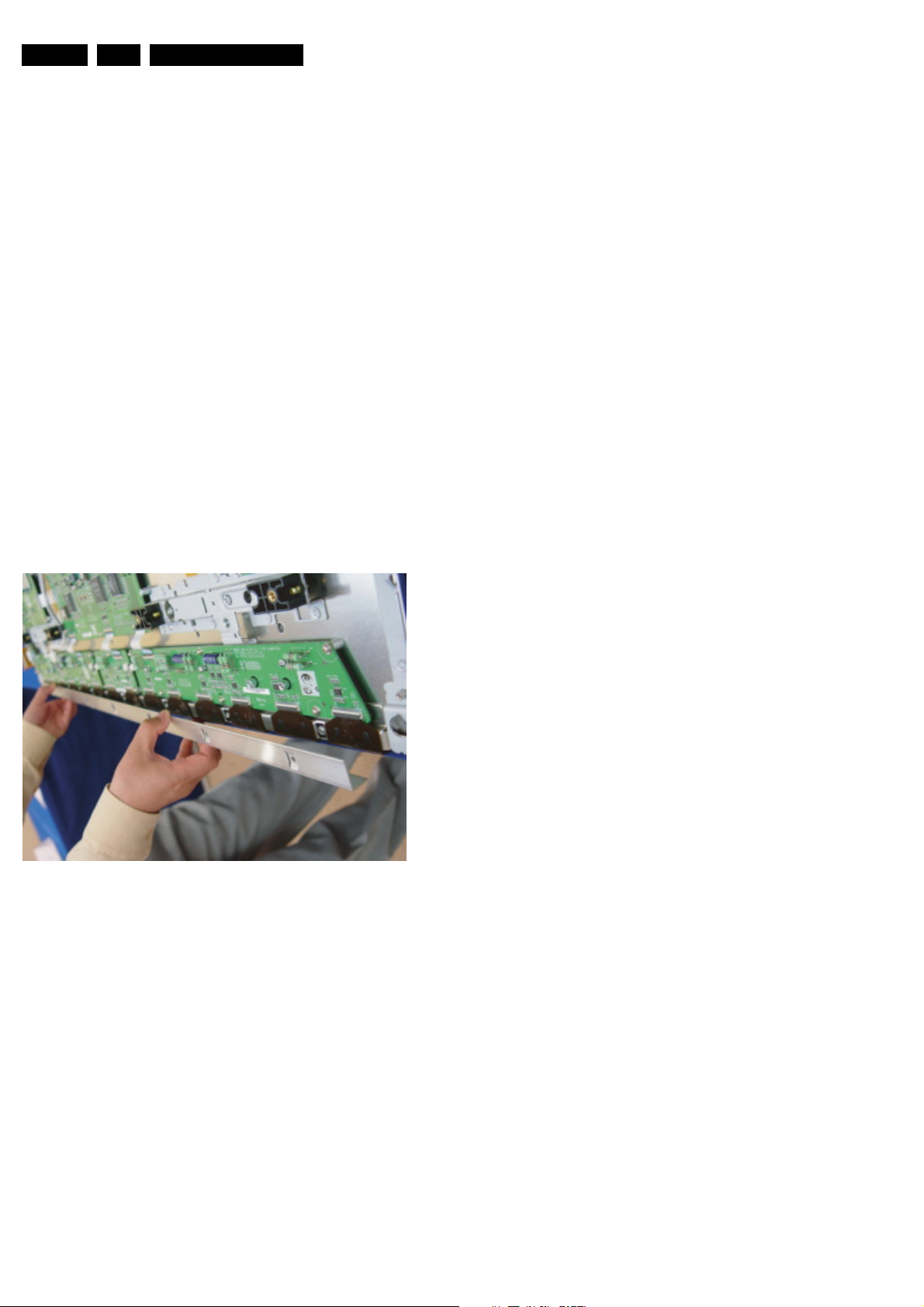
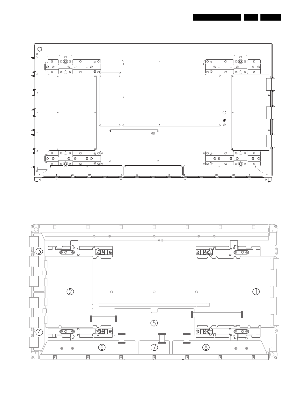
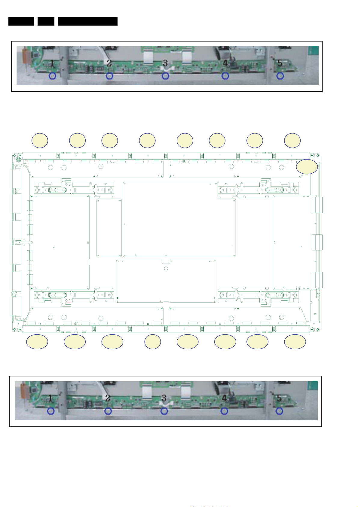
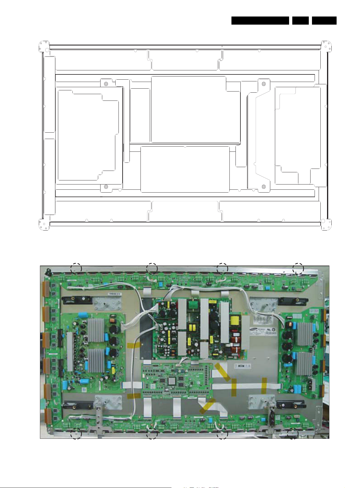
1. Depending on the model (see “Photo 2” per model.):
– 42" SD v3 - Remove the screws in order of 2-3-5-7-1-
4-6 (and 10-11-13-16-9-12-14 for HD) from heat sink
and then remove heat sink (Photo 1).
– 42" SD v4 - Remove the screws in order of 2-4-1-5-3
from heat sink and then remove heat sink (Photo 1).
– 42" HD v3, 37" SD v4, 50" HD v3 - Remove the
screws in order of “Centre - Left Side - Right Side” from
heat sink and then get rid of heat sink (Photo 1).
– 50" HD v4 - Remove the screws in order of 2-3-1-4
from heat sink and then remove heat sink (Photo 1).
2. Remove the TPC, FFC, and power cable from the
connectors.
3. Remove all the screws from the defective board.
4. Remove the defected board.
Note: When replacing the Logic board or Y-main board for
a lead-free (Pb-free) board, always replace them together.
(this is only valid for the 37" SD v4 displays!)
5. Replace the new board and then screw tightly.
6. Clean the connectors.
7. Re-connect the TCP, FFC, and power cable to the
connector.
8. Re-assemble the TCP heat sink. Use the same screw
mounting order as described above
Mechanical Instructions
Caution: If you screw too tight, it is possible to damage the
Driver IC of the TCP.
Figure 4-9 Photo 1 - Heatsink removal
Page 21
Mechanical Instructions
Left
Centre Right
4 6 17 532
EN 21SDI PDP 4.
Figure 4-10 Photo 2 - 37" SD v4
Figure 4-11 Photo 2 - 42" SD v2 and v3
Page 22
EN 22 SDI PDP4.
F_14991_028.eps
030805
1
2
3
4
5
XYG Z[G \G]G ^_
`XW XXXY X[G X\X] XZ
YY
1
2
3
4
5
Mechanical Instructions
Figure 4-12 Photo 2 - 42" SD v4
Figure 4-13 Photo 2 - 42" HD v3
Figure 4-14 Photo 2 - 42" HD v4
F_14991_028.eps
030805
Page 23
Mechanical Instructions
Left Centre Right
F_14991_029.eps
030805
ཛGཛྷཝཞ
ཛ
G
ཛྷཝཞ
G
EN 23SDI PDP 4.
Figure 4-15 Photo 2 - 50" HD v3
Figure 4-16 Photo 2 - 50" HD v4
Page 24
EN 24 SDI PDP4.
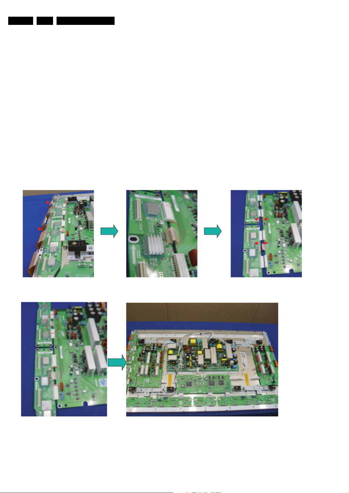
4.1.5 Exchange YBU, YBL and YM board
1. Separate all the FPC connector s of YBU (Y-Buffer upper)
and YBL (Y-Buffer lower). See “Photo 1”.
2. Separate all the connector of CN5001 and CN5008 from YMain. See “Photo 2”.
3. Loosen all the screws of YBU, YBL, and YM. See “Photo
3”.
4. Remove the board from chassis.
5. Remove the connector of CN5006 and CN5007 among
YBU, YBL and YM.
6. Remove the YBL and YBU from Y-main.
7. Remove the defected board.
Note: When replacing the Logic board or Y-main board for
a lead-free (Pb-free) board, always replace them together.
(this is only valid for the 37" SD v4 displays!)
8. Re-assemble the YBU and YBL to the Y-Main.
9. Connect the connector of CN5006 and CN5007 among
YBU, YBL and YM. See “Photo 4”.
10. Arrange the board on the chassis and then screw to fix.
11. Connect the FPC and YM of panel to the connector. See
“Photo 5”.
12. Supply the electric power to the module and then check the
waveform of the board.
13. Turn “off” the power after the waveform is adjusted.
Mechanical Instructions
Figure 4-17 Photo 1, 2, and 3: Dis-assembly of YBU, YBL, and YM
Figure 4-18 Photo 4 and 5: Re-assembly of YBU, YBL, and YM
Page 25
Service Modes, Error Codes, and Fault Finding
F_14991_031.eps
030805
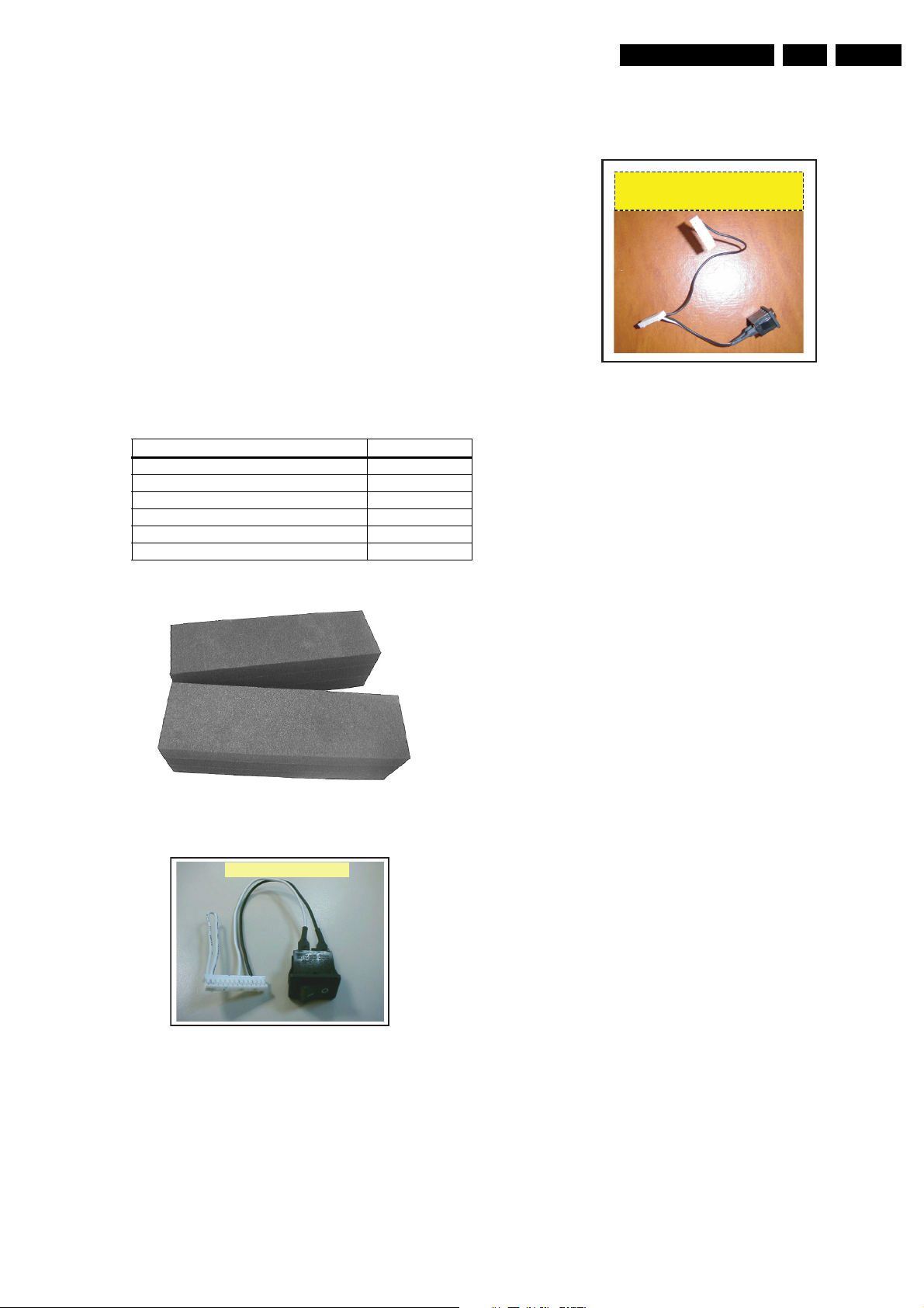
3122 785 90760
F_14991_030.eps
030805
3122 785 90770
5. Service Modes, Error Codes, and Fault Finding
Index of this chapter:
5.1 Repair Tools
5.2 Fault Finding
5.3 Defect Description Form
5.1 Repair Tools
5.1.1 ComPair
For the v3 and v4 models, it will be possible to generate test
patterns with ComPair. The ComPair interface must be
connected to the Logic Board with the special interconnection
cable (see table below for the order code).
5.1.2 Other Service Tools
Table 5-1 Overview Service tools
Figure 5-3 V3 jig
Service Tools
Jumper J8002 + V2 JIG connector kit 3122 785 90760
V3 JIG connector + for SDI panel repair 3122 785 90770
Jumper J8002 to be used in connector kit 3122 785 90780
V2 JIG connector to be used in conn. kit 3122 785 90790
ComPair / SDI interconnection cable 3122 785 90800
Foam buffers (2 pcs.) 3122 785 90581
Order Code
EN 25SDI PDP 5.
Figure 5-1 Foam buffers
Figure 5-2 V2 jig
Page 26
EN 26 SDI PDP5.
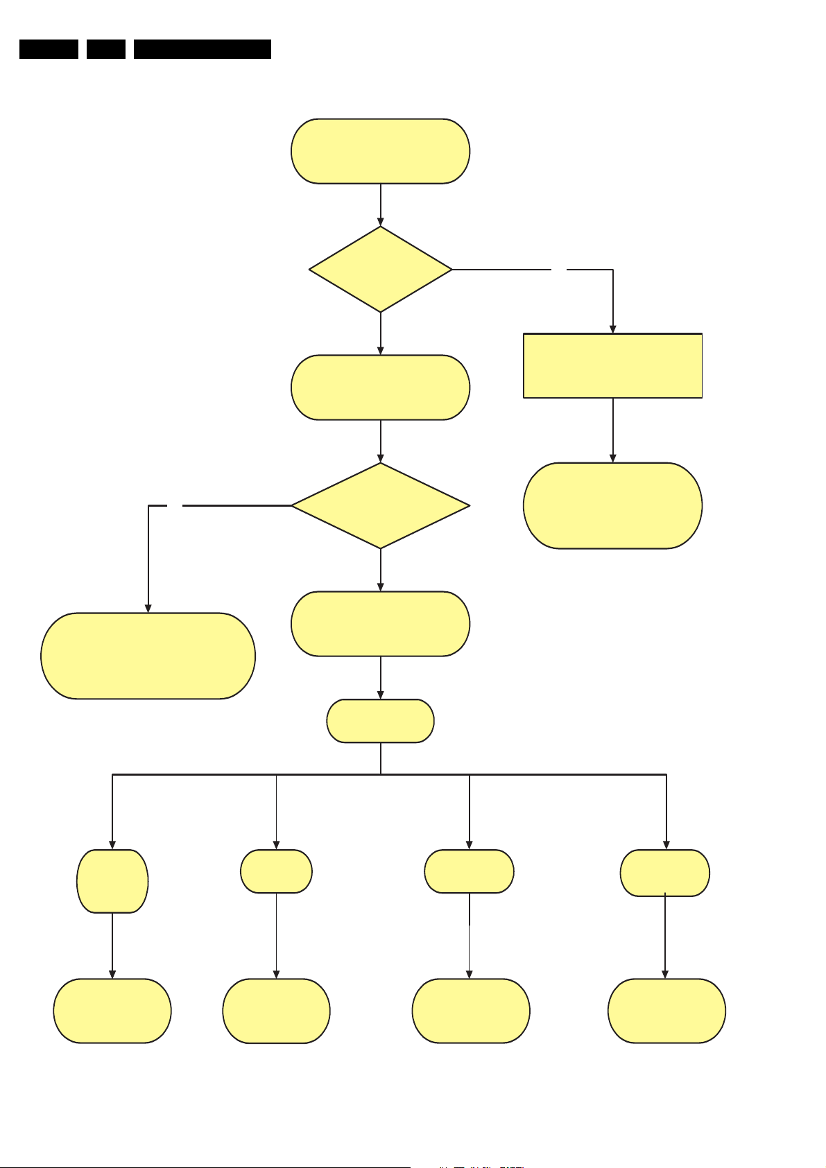
Chassis ?
FM242
Repair Scenario
42” SD v2
Repair Scenario
42”/50” SD/HD v3
First check complete TV set.
Fault Symptom?
Check if LVDS from SCAVIO
or SSB board is OK.
Use LVDS Tool when possible.
Output of SSB / SCAVIO
is OK?
SDI repair Scenario.
Fault finding: Display fault.
Repair Philips application.
See chassis related Service Manuals
No
Power Supply
is working ?
Go to
“Power Supply Check”
& repair scenario
with Philips application
or PDP as stand alone check.
No
FTP1.1
F21RE
FM24_AB
LC4.7
FTP2..2
LC4.7
Repair Scenario
42”/50” SD/HD v4
Repair Scenario
37” SD v4
Power supply is not working.
No voltage output.
F_14991_036.eps
280306
FTP2..4
LC4.9
BP2.x
5.2 Fault Finding
Service Modes, Error Codes, and Fault Finding
Figure 5-4 Which repair scenario?
Page 27
Service Modes, Error Codes, and Fault Finding
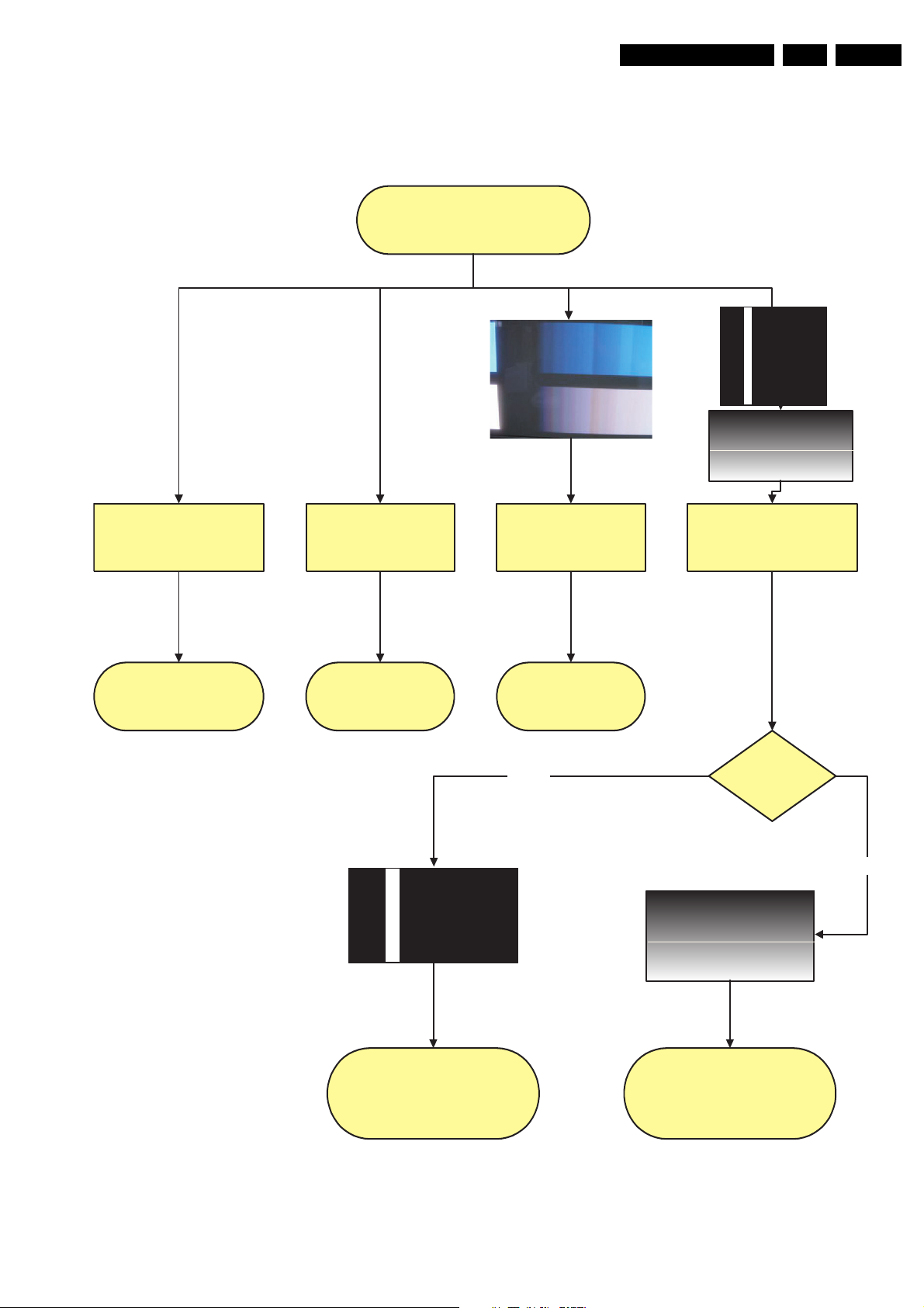
First check complete TV set.
Fault Symptom?
EN 27SDI PDP 5.
No Voltage output
Operating Voltages don´t exist
Go to
“Power Supply Check”
flowchart
(version dependent)
Operating Voltages exist,
but No Display
Go to
“No Display”
flowchart
Abnormal Display, not
open or short Lines
Go to the
“Abnormal Display”
flowchart
Vertical
Some horizontal or Vertical
Lines don´t exist on the
Display.
Sustain open
Horizontal or
Vertical Lines?
Horizontal
Is related to Logic adress Buffer.
Go to
“Address Open / Short”
flowchart
Figure 5-5 Fault symptom overview (complete TV set)
Is related to X-Main, Y-Main
Go to
and Y-buffer.
“Sustain Open / Short”
flowchart
Page 28
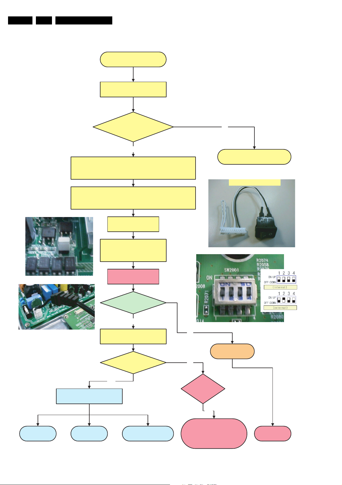
EN 28 SDI PDP5.
Repair 42 SD v2
as stand alone
PDP identification =
S42SD-YD06
Check PDP Type number
For FM242 disconnect and remove SCAVIO Board.
For FTP1.1 disconnect and remove SSB and Audio Board.
Connect Jig connector to CN8002 (13 pins).
Short circuit between pin 1 & 2 = On/Off switch (vacation switch).
Switch between pin 8 & 11 standby line switch.
Y
No
Go to v3 or v4 repair scenario.
Short the Jumper J8002.
Set the DIP switch 2 “on”.
.
the Logic main board to “off”.
Plug in the Power cord.
Switch Jig connector switch “on”.
Green Stby LED
8003 is “on” ?
Green LEDs 8001
& 8002 are “on”?
Ye s
Standby Supply
is defective.
Replace Power
supply board.
No
Go to fault finding part:
Ye s
Go to “Power Supply Check”
repair procedure for v2 versions.
Switch “on” via Jig connector
switch.
Protection
LED8004 is “on”?
Ye s
No
No Display Abnormal Display
Some horizontal or
Vertical Lines don´t exist
3122 785 90760
Service Modes, Error Codes, and Fault Finding
Figure 5-6 Repair scenario v2 stand alone panels
Page 29
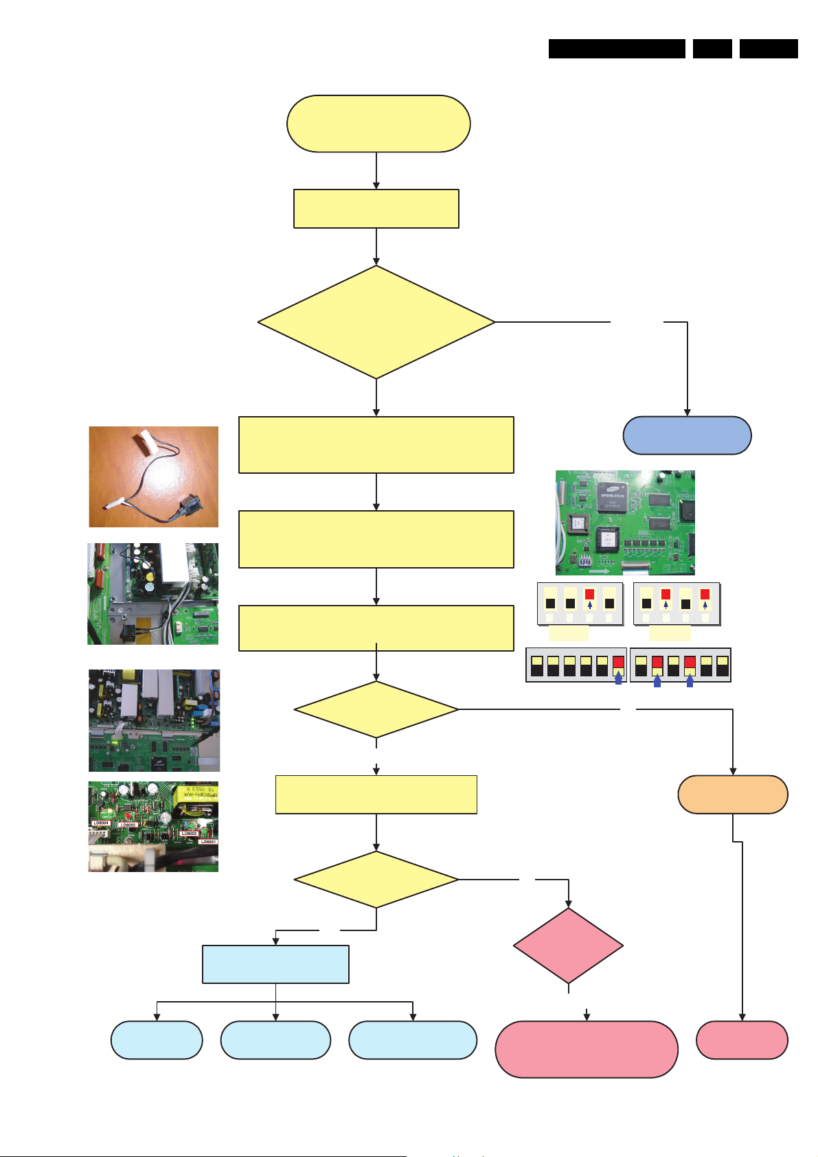
Service Modes, Error Codes, and Fault Finding
Repair 42" & 50" SD/HD v3
as stand alone
Check PDP type number:
PDP identification =
S42SD-YD05 or YB03?
S42AX-XD02 or XB01?
S50HW-XD03 or XB02?
Other PDP
type
EN 29SDI PDP 5.
3122 785 90770
CN
9004
Switch
Sub
PSU
CN9005
Disconnect and remove SSB FTP2.2 or LC4.7 board.
Remove plastic frame to have acces to all boards
Connect Jig connector with switch to Sub PSU 9004/9005
Set DIP switch 3 to internal mode.
Position of DIP Switch Int or Ext is indicated on board.
Connect Mains to PSU board (CN8001 on PSU, use
mains filter).
Switch PDP “on’ with switch.
Green Stby LED
LD8004 is “on” ?
Ye s
Switch Jig connector switch “on”.
1 2 3 4
1 2 3 4
Internal
Internal
Go to v2/v4 repair scenario
1 2 3 4
1 2 3 4
External
External
No
Standby Supply
is defective.
42-inch
50-inch
No Display
Ye s
Go to fault finding part:
Abnormal Display
Figure 5-7 Repair scenario 42"/50" SD/HD v3 stand alone panels
Green LED LD8001
& LD8003 are “on”?
Some horizontal or
Vertical Lines don´t exist
No
Protection
LD8002 is “on”?
Ye s
Go to “Power Supply Check”
repair procedure for v3/v4 versions.
Switch “on” via Jig connector switch.
Replace Power
supply board.
Page 30
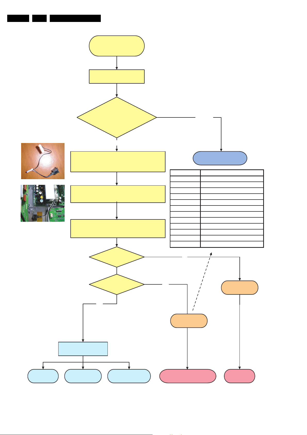
EN 30 SDI PDP5.
LED signature Detected error condition
1 time V_A OVP, UVP
2 times V_G OVP, UVP
3 times D5VL OVP, UVP
4 times D3V3 OVP, UVP
5 times V_S OVP, UVP
6 times V_SET OVP, UVP
7 times V_SCAN OVP, UVP
8 times VE OVP, UVP
9 times Over-temperature (> 105
o
C)
10 times DC_PROT
11 times ALT_SIG
12 times TIME_OVER
Service Modes, Error Codes, and Fault Finding
Repair 37" SD v4
as stand alone.
Check PDP type number:
3122 785 90770
CN
9004
Switch
Sub
PSU
CN9005
PDP identification =
S37SD-YD02?
Ye s
Disconnect and remove SSB (and other Philips applications).
Remove plastic frame to have acces to all boards
- Connect Jig connector/switch to Sub PSU pos. 9004/9005
- Insert jumper CN2008 on Logic Brd for full white picture.
This is the ONLY jumper that must be placed!
- Connect Mains to PSU board (CN8001 on PSU, use
mains filter).
- Switch PDP “on’ with switch.
2. Insert jumper at CN8012 for stand alone application
Green LEDs
LD8001, LD8003
Other PDP
type
Locate the appropriate flowchart
for the PDP version
No
(jumper setting ok?)are “on” ?
PSU okay. If display problems,
go to fault finding part:
No Display Abnormal Display
Protection
LED BLD8001 is
blinking?
No
Some horizontal or
Vertical Lines don´t exist
Figure 5-8 Repair scenario 37" SD v4 stand alone panels
Ye s
repair procedure for v4 versions.
Determine defective
part via error table.
Go to “Power Supply Check”
Power Supply
is defective.
Replace Power
Supply board.
F_14991_039.eps
280306
Page 31
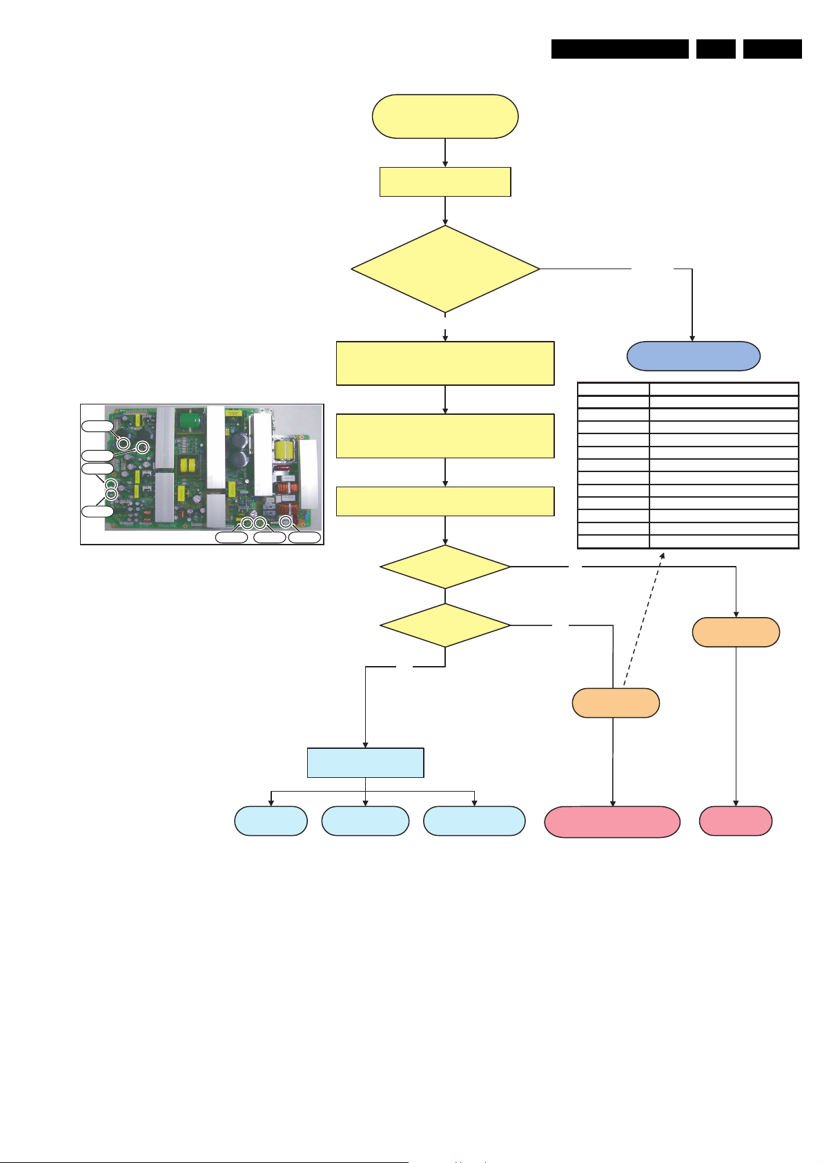
Service Modes, Error Codes, and Fault Finding
Repair 42" & 50" SD/HD v4
Check PDP type number:
PDP identification =
S42SD-YD07?
S42AX-YD01?
S50HW-XD04?
Disconnect and remove SSB.
Remove plastic frame to have acces to all boards
- Insert jumpers at J8003, J8004 (and BJ8902 for
stand alone application without Logic brd).
- Insert jumper CN2012 on Logic Brd for full white picture.
Connect Mains to PSU board
(CN8001 on Power Supply, use mains filter).
Green LEDs
are “on” ?
8002, 8001, BD8903 (on PSU)
Other PDP
type
Power Supply
is defective.
Replace Power
Supply board.
No
go to fault finding part:
PSU okay. If display problems,
Go to “Power Supply Check”
repair procedure for v4 versions.
Ye s
No
Ye s
No Display Abnor mal Display
Some horizontal or
Vertical Lines don´t exist
F_14991_037.eps
280306
as stand alone.
Determine defective
part via error table.
Protection
LED BD8903 is
blinking?
LED signature Detected error condition
1 time V_A OVP, UVP
2 times 12V OVP, UVP
3 times V_SCAN OVP, UVP
4 times D3V3 OVP, UVP
5 times V_S OVP, UVP
6 times V_G OVP, UVP
7 times V_SET OVP, UVP
8 times V_E OVP, UVP
9 times Over-temperature (> 105
o
C)
10 times PFC_OK UVP (> 330 V)
11 times 5V2 OVP or Active DC_PROT
13 times D5VL OVP, UVP
LED8002 LED8001 CN8001
BD8903
BJ8902
right pos.
J8004
J8003
(jumper setting ok?)
Locate the appropriate flowchart
for the PDP version
EN 31SDI PDP 5.
Figure 5-9 Repair scenario 42"/50" SD/HD v4 stand alone panels
Page 32
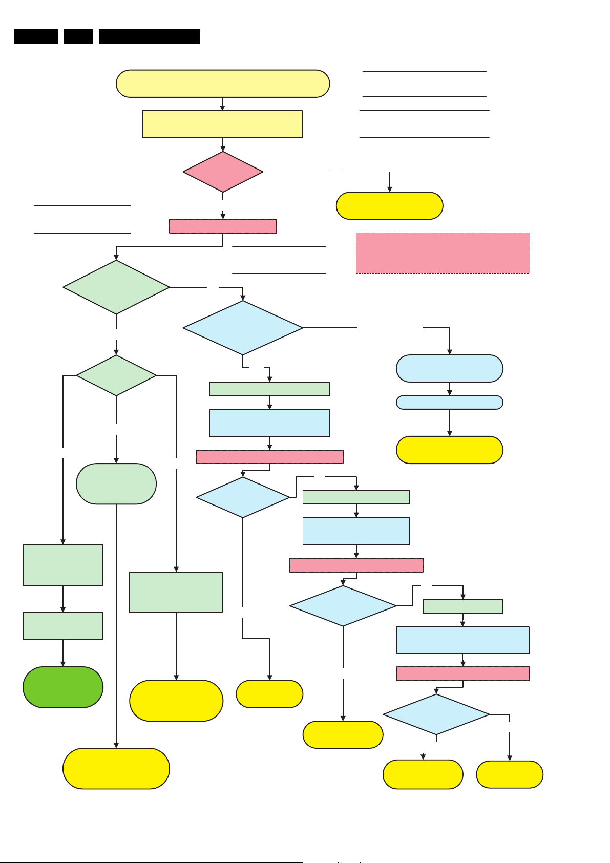
EN 32 SDI PDP5.
Power Supply Check (v2 versions)
LED8003
Stby is ON?
Green LEDs
8001, 8002
are ON?
Connect set to mains.
Switch ON (with vacation switch)
Check SMPS outputs
Vs, Va, Vset, Ve, Vsc
see Sticker
Ye s
NO
Check CN8004 / 2pin
connector 220V AC
Check F8002
Fuse 250V/8A
ON/OFF relay
RLY8001/8002 acts?
Switch ON via 1 or 2
Check Protection Red
LED8004
Ye s
No
Disconnect VA Logic Buffer
CN8010 / CN8011
Disconnect X-main CN8007
SMPS shuts down?
Red LED8004 is ON.
Protection
Reconnect mains. Switch ON via 1 or 2
Standby supply is defective.
Replace PSU
Ye s
Activate SAM
or SDM
Disconnect mains cord
Disconnect Y-main CN8008
SMPS is working? Disconnect mains cord
No
Disconnect mains
Reconnect mains. Switch ON via 1 or 2
SMPS is
working?
No
Replace
Y-Main board
Replace
X-Main board
SMPS is
working?
No
Replace defective
Logic Buffer board
Ye s
Reconnect mains. Switch ON via 1 or 2
Replace PSU
Ye s
Check Stanby Line pin 11
on CN8002 must be LOW.
Go to repair scenario
as stand-alone
LED on Logic
main board ?
Data communication
from Philips
application to Logic
mains is OK.
Blinking
Continous ON, means no
data communication over
LVDS Cable.
Green LED 8001,
8002
& Red LED are OFF
Ye s
No switch ON of PSU
Switch from standby to on;
1) Via RC when Philips application is in.
2) Via Switch-On-Jig connector when Philips
application is removed
Discharge capacitors on Power supply, before
reconnecting X, Y or Logic Buffer board, use
2K4/10W discharge resistor
Go to repair scenario
as stand-alone
On
Check Power supply
on Logic-Main board.
3.3V and 5V
If Power Supply on Logic
mains is not OK, change PSU
or Logic main board
Off
Service Modes, Error Codes, and Fault Finding
Figure 5-10 Power Supply Check for v2 models
Page 33
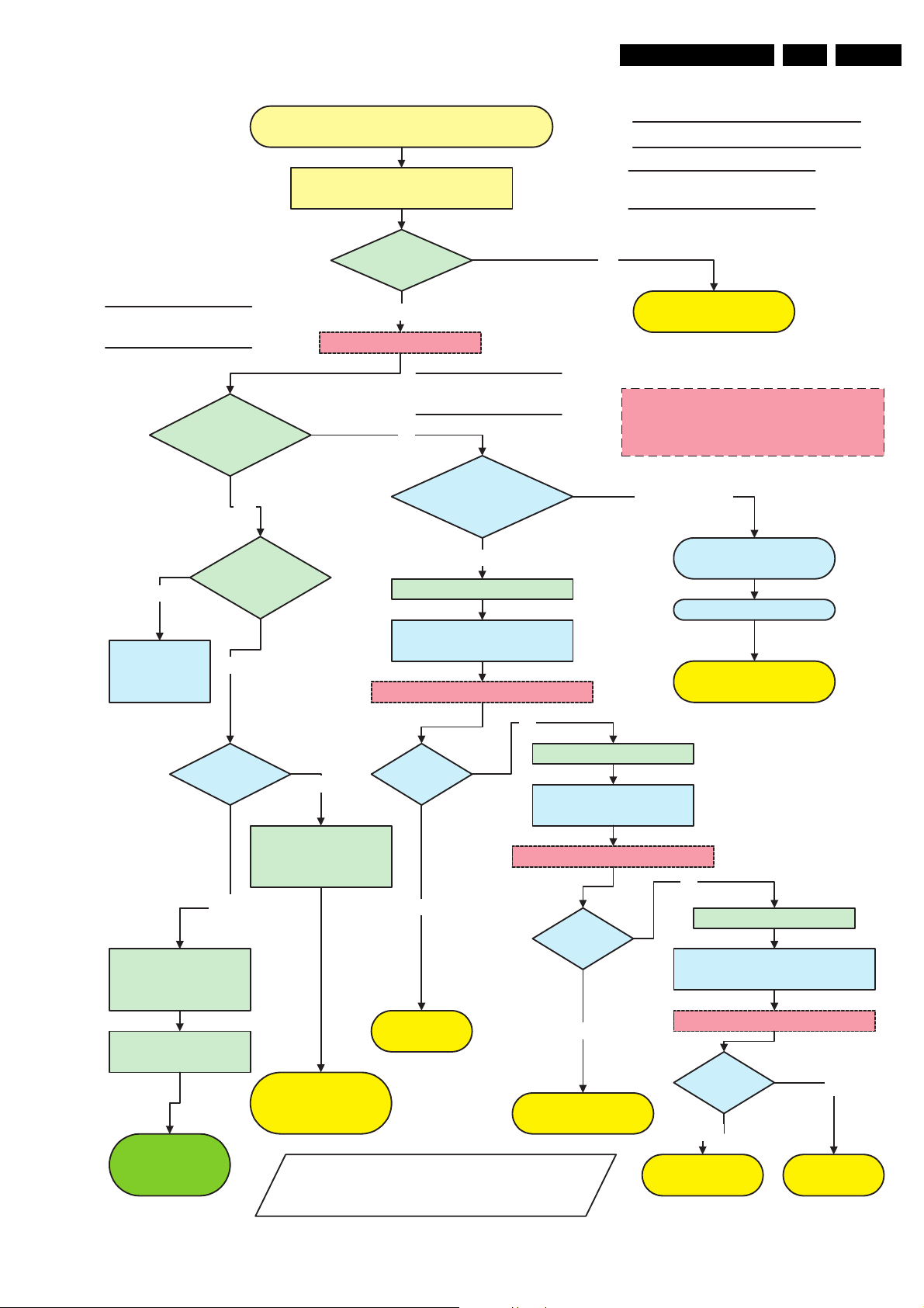
Service Modes, Error Codes, and Fault Finding
EN 33SDI PDP 5.
ON/OFF relay
RLY8001/8002 acts?
Green LEDs
8001, 8002
are ON?
LEDs 3.3V and 5V
Off
on Logic main board?
Power Supply Check (v3 versions)
Connect set to mains.
LED8003
Stby is ON?
Ye s
Switch ON via 1 or 2
Check Protection Red
No
SMPS shutsdown?
Ye s
Red LED8004 is on.
Protection
Disconnect mains cord
LED8004
Ye s
Check CN8001 / 2pin connector 220V AC
Check Fuse F800 / F8002 / F8003
NO
Standby supply is defective.
Replace PSU
Switch from standby to on;
1 Via RC when Philips application is in.
2 Via Switch-On-Jig connector when Philips
application is removed
Green LED 8001,
8002
& Red LED are OFF
Check Stanby Line pin 13
on CN8004 must be LOW.
No switch ON of PSU
Check Power
supply on Logic-
Main board.
Data communication from
Philips application to Logic
mains is OK.
Activate SAM
or SDM
Check SMPS outputs
Vs, Va, Vset, Ve, Vsc
see Sticker
On
Data LED ON
Logic Main ?
Blinking
On
Continous on, means no
data communication over
LVDS Cable.
Go to repair
scenario
as stand-alone
Discharge capacitors on Power supply,
before reconnecting X, Y or Logic Buffer
board, use 2K4/10W discharge resistor
Disconnect Y-main CN8003
Reconnect mains. Switch ON via 1 or 2
No
Disconnect mains cord
SMPS is
working?
Disconnect X-main CN8002
Reconnect mains. Switch ON via 1 or 2
Ye s
SMPS is
working?
Replace
Y-Main board
Replace
X-Main board
Ye s
Go to repair scenario
as stand-alone
No
Disconnect mains
Disconnect VA Logic Buffer
CN8005 / CN800x
Reconnect mains. Switch ON 1 or 2
SMPS is
working?
Ye s
Replace defective
Logic Buffer board
No
Replace PSU
Figure 5-11 Power Supply Check for v3 models
Page 34
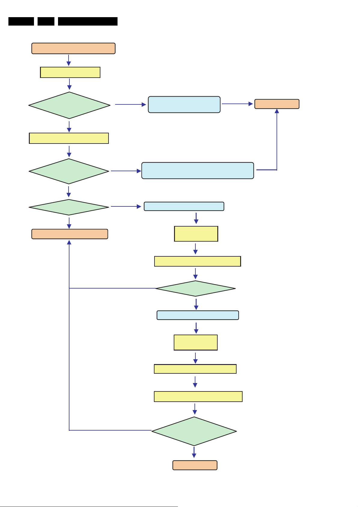
EN 34 SDI PDP5.
ΠΨΖΣ΄ΦΡΡΝΪʹΙΖΔΜ·ΙΚΝΚΡΤ
ʹΠΟΟΖΔΥΠΣΤΖΥΥΠ
·ΦΥΡΦΥ
·ΠΝΥΒΘΖͰ
΄ΥΒΟΕΓΪΤΦΡΡΝΪΚΤ
͵ΖΗΖΔΥΚΧΖ
Ϳ
΄ΨΚΥΔΙͿͲΔΥΚΧΖͽΠΨ
ΊΖΤ
Ϳ
ͽͶ͵
ΚΤͿͰ
ͲΥͽͶ͵ΗΗͷʹΙΖΔΜ
ͲΥͽͶ͵ͿΗΗ
ΊΖΤ
ͳ͵ͳΝΚΟΜͰ
ΊΖΤ
΄ΖΧΖΣΒΝͳΝΚΟΜͰΣΠΥΖΔΥΚΠΟΥΒΓΝΖ
Ϳ
ͲΝΝΕͺΤΔΠΟΟΖΔΥ
ͳ͵
΄ΆͿΠΣΞΒΝΚΥΪ
ͳ͵ͳΝΚΟΜͰ
ʹͿʹΠΟΟΖΔΥΒΟΕ΄ΨΚΥΔΙͿ
΄ΖΧΖΣΒΝͳΝΚΟΜͰΣΠΥΖΔΥΚΠΟΥΒΓΝΖ
Ϳ
ΊΖΤ
ͲΝΝΕͺΤΔΠΟΟΖΔΥ
ͳ͵
ʹͿʹΠΟΟΖΔΥΒΟΕ΄ΨΚΥΔΙͿ
ͳͻʹΠΟΟΖΔΥͻΦΞΡΖΣ
ͲΝΝΠΦΥΡΦΥ
ΧΠΝΥΒΘΖʹΙΖΔΜͰ
ΊΖΤ
Ϳ
΄ΆΖΡΝΒΔΖ
΄ΆΖΡΝΒΔΖ
ΞΒΚΟ
F_14991_064.eps
120206
Service Modes, Error Codes, and Fault Finding
Figure 5-12 Power Supply Check for v4 models
Page 35
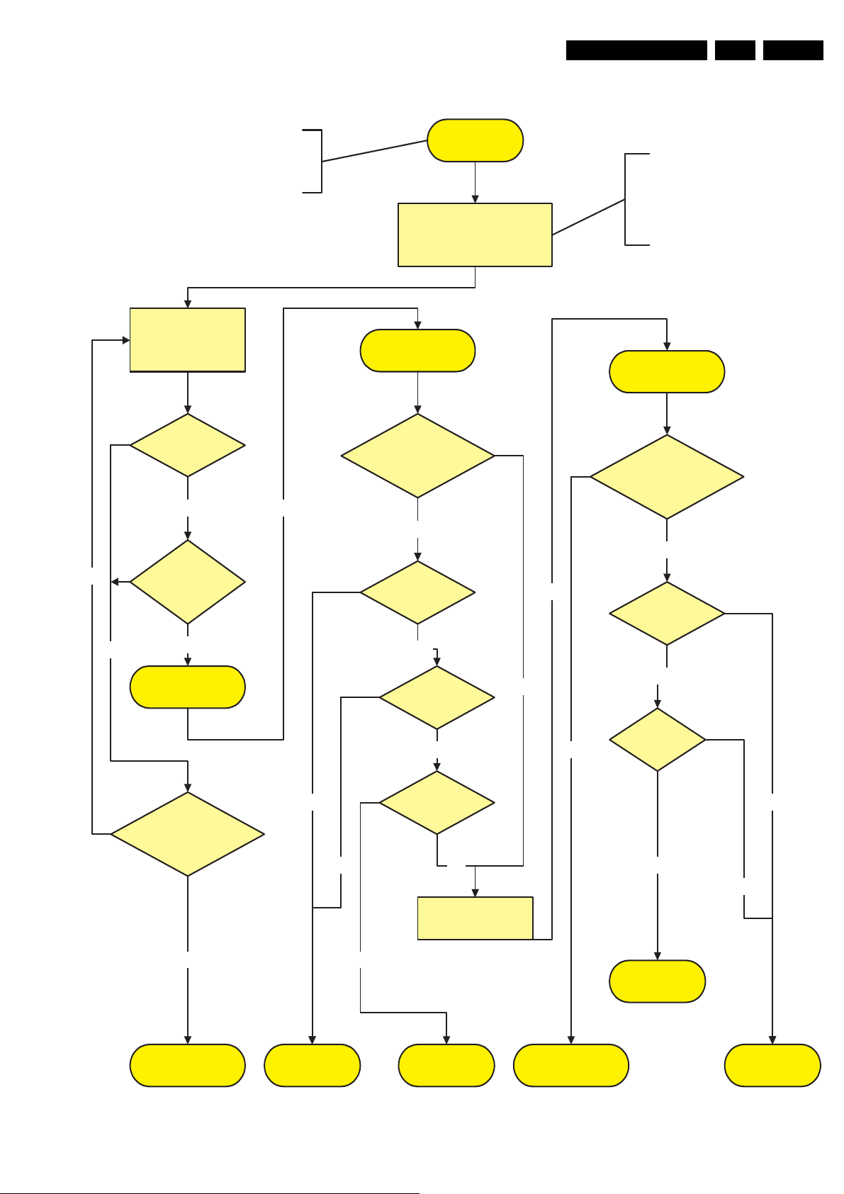
Service Modes, Error Codes, and Fault Finding
No Display
Check Logic Main
Dip switch is on
Internal mode!
LED blinks?
Logic main
normal state
Ye s
OK
Check Fuse ?
Check FET
Short?
Y-Main & Y-buffer
normal state
Not OK
OK
No
Check Fuse ?
Check FET
Short?
No
Not OK
OK
Bring set in
repair set-up as standalone
Scavio or SSB is
disconnected and removed.
Power supply will be started-
up with Jig connector and
DIP switch on Logic Main is
on internal mode.
No
Open
Ye s
Replace the Logic-
main board
Replace the
Y-main board
Replace the
X-main board
Open
Ye s
Operating voltages exist, but there
is no Display.
No Display is related with Y-Main,
X-Main or Logic-main board
Check Power
supply on Logic mains.
3V3 & 5V.
Not OK
OK
OK
Waveform
on Y Buffer
test point ?
Waveform
on X-board
test point ?
Replace PDP Panel
OK
Check V-Sync
on test point logic
main board
OK
OK
Check Y-Main board
X-Main
normal State
Check X-Main board
Check
Y Buffer Uper
and Lower?
OK
Replace Y buffer
Not OK
EN 35SDI PDP 5.
Figure 5-13 Fault symptom: “No Display”
Page 36
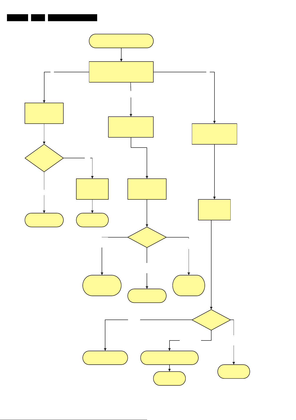
EN 36 SDI PDP5.
Abnormal Display
Exept for Horizontal or Vertical Lines
Check FFC
(Flat Foil Cables) between
Logic-main, X-main and Y-main
Logic-Main
Observation of
abnormal Display
Y-Main Check
Check Fuses and FET
X-Main Check
Check Fuses and FET
Regular abnormal
pattern
Logic main
normal state
Replace PDP
Ye s
No
Replace the Logic-
main board
Check X
Wavefo rm
Check Ramp
waveform on Y-board
(buffer)
1
2
3
Wavefo rm?
Go to X-Main board
Check
Check voltages.
Adjust Y waveform
Check voltages.
Replace Y-Main
board
Not
correct
Waveform is
OK
No
waveform
Wavefo rm?
X main board seems to be OK.
Check supply voltages or
replace X-Main board.
Replace X-Main
board
Not
correct
Waveform is
OK
Waveform not
OK
Replace PDP
Service Modes, Error Codes, and Fault Finding
Figure 5-14 Fault symptom: “Abnormal Display”
Page 37
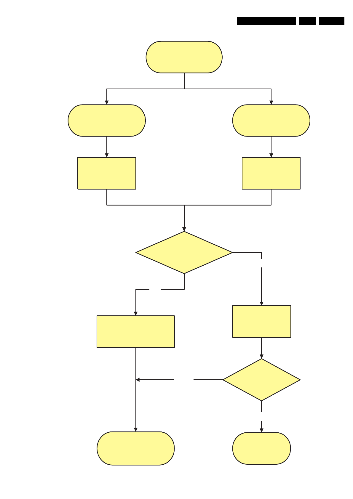
Service Modes, Error Codes, and Fault Finding
Sustain Open / Short
Y-FPC
Sustain open
Change Y-Buffer
Upper or Lower
Horizontal Lines
Some horizontal lines don´t
exist on Display
After changing buffer,
recheck the status
Done
Defect is from buffer
Replace the panel (PDP)
There is a defect on FPC
OK
OK
Horizontal lines
Some horizontal lines appear
to be linked on Video
Y-FPC
Sustain Short
Check connections
Y-buffer up & Low
Check FFC
FPC damaged or connection
to PDP
Nok
Not OK
EN 37SDI PDP 5.
Figure 5-15 Fault symptom: “Sustain open / short”
Page 38
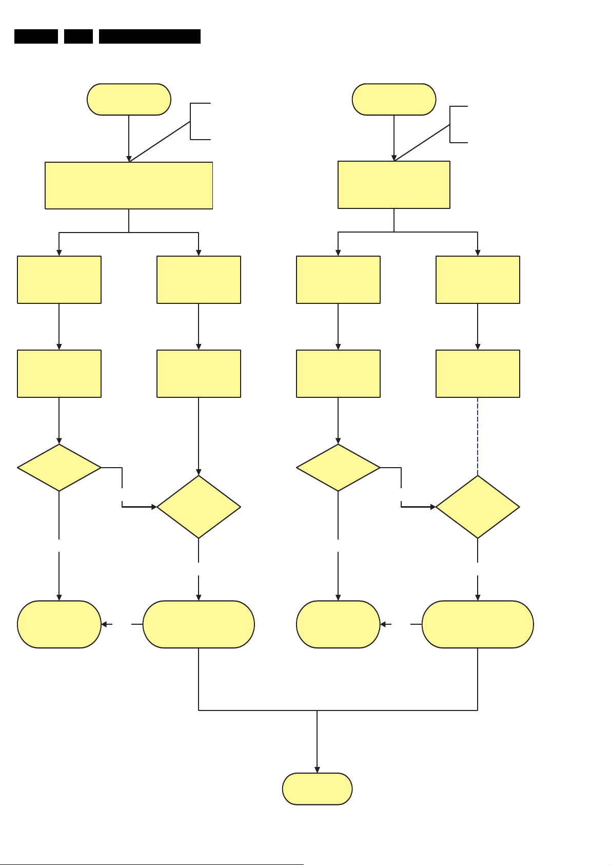
EN 38 SDI PDP5.
Adress Open
Line Open
Data Block Open
1/2 or 1/4 of Display is missing
COF Block Open
Logic Main / FFC
Check or change
interconnections
Logic Buffer
Check Va Supply
Check and / or
change E / F / G
Buffer
What is the status of
Open?
1 Line
or 1 Block
Half Block /
Half of Screen
Replace PDP
Replace Logic-Main/
Adress Buffer E or F or G/
FFC
Ye s
No
Ye s
Done
Adress Short
Line short
Data Block short
NOK
Adress open is related with
Logic Main, Logic Buffer
, FFC, TCP and so on.
Adress short is related with
Logic Main, Logic Buffer,
FFC, TCP and so on.
Logic Main / FFC
Check or change
interconnections
Logic Buffer
Check Va supply
Check and / or
change E / F / G
Buffer
What is the status of
Short?
1 Line
or 1 Block
Half Block /
Half of Screen
Replace PDP
Replace Logic-Main/
Adress Buffer E or F or G/
FFC
Ye s
No
Ye s
NOK
Service Modes, Error Codes, and Fault Finding
Figure 5-16 Fault symptom: “Address open / short”
Page 39
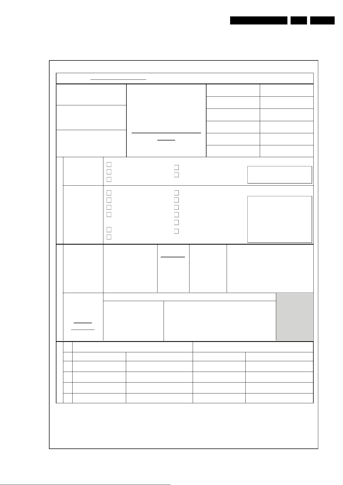
Service Modes, Error Codes, and Fault Finding
F_15590_115.eps
050407
Defect Description Form LCD PLASMA v4.0 final Date last modified: 28/03/2006
To be filled in by WORKSHOP / WORK CENTER
Country:
Customer Account nr.:
Job sheet nr.:
PHILIPS
LCD & Plasma
DEFECT DESCRIPTION
FORM
Type nr./Model nr. set
Serial nr. set
Type nr. display
Serial nr. display
Part nr display (12nc)
Return number
GENERAL REPAIR DATA
Condition
Symptom(s)
Constantly
Intermittently
After a while
In hot environment
In cold environment
Other:
No backlight
No picture
Picture too bright
Scratches (LCD only acc.
Pixel criteria sheet V4.0)
Only partial picture
Unstable picture
Flickering / flashing picture
Lines across/down image
Inactive row(s)
Inactive column(s)
Missing colour(s)
Light leakage
Other:
PANEL REPAIR
Pixel
Defect(s):
Symptoms
Out of
warranty
Dark dots
Bright dots
Qty of dots:
Mark
Defect(s):
These
symptoms
are not
claimable.
Following defect symptoms are out of warranty:
Broken glass / Broken
polarizer
Scratch(es) on display /
polarizer
Number of dark/bright pixels within spec.
Burn in (Plasma TV) / Sticking image (LCD TV)
MURA
-
-
-
-
-
BOARD REPAIR
Defect Board New Board
Spare Part Nr. Serial Nr. Spare Part Nr. Serial Nr.
1.
2.
3.
4.
Note 1: The defective LCD-panel / PDP needs to be returned in the same packaging as the new part was send. If not
the warranty claim will be rejected.
Owner: PHILIPS CE EUROSERVICE
DE10WEG
5.3 Defect Description Form
This form must be used by the workshops for warranty claims:
EN 39SDI PDP 5.
Figure 5-17 Defect Description Form (DDF)
Page 40
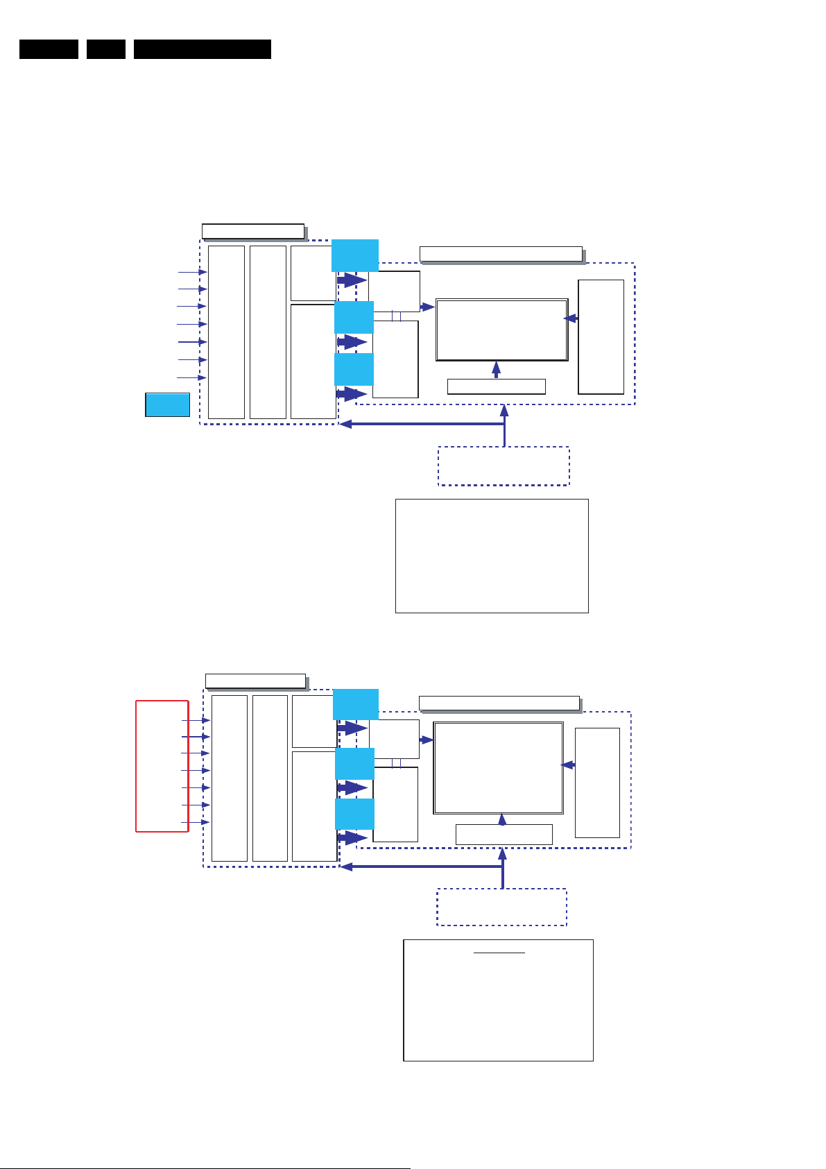
EN 40 SDI PDP6.
- Vcc : Voltage for Logic Control
- Vdd : Voltage for FET driver
- Va : Voltage for address pulse
- Vs : Voltage sustain pulse
- Vsc : Voltage for scan pulse
- Ve : Voltage for X ramp pulse
- Vset : Voltage for Y ramp pulse
Reference
VsVa
Vcc
Enable
Hsync
DCLK
Display
Data
Driver
Timing
Sca n
Timing
Vdd
Vset Vsc
Ve
LVDS
Interface
Data Controller
Input Data Processor
Driver
Timing Controller
DRAM
Row
Driver
Y Pulse
Generator
852 x 480 Pixels
852 x 3 x 480 Cells
Column Driver
X Pulse
Generator
DRIVER CIRCUIT & PANEL
LOGIC CONTROL
DATA_R
8 Bits
DATA_G
8 Bits
DATA_B
8 Bits
Vsync
852× 480 Pixels
852× 3× 480 Cells
P
Y
u
l
s
e
Ge tarenor
oRw
rD
ive
r
VsVa
V5
Vs ync
Enable
Hsync
DCLK
ARDM
Display
Data
irDver
Timi gnCt
n
oroller
Driver
Timing
Scan
Timing
Vdd
DATA_R
8Bits
Column Driver
Reference
-V3.3 :
-V5 :
-Vdd :
-Va :
-Vs :
-Vsc :
-Ve :
-Vset :
LOGIC CONTROL
DRIVER CIRCUIT & PANEL
DATA_G
8Bits
DATA_B
8Bits
In tupDataProcsesor
aD
t
aoCntor ller
PXulse
eGn
era
tor
Vset Vsc
Ve V3.3
LVDS
Voltage for LOGIC Control
Voltage for COF driver
Voltage for FET driver
Voltage for address pulse
Voltage for sustain driver
Voltage for scan pulse
Voltage for X ramppulse
Voltage for Y ramppulse
Block Diagrams, Test Point Overview, and Waveforms
6. Block Diagrams, Test Point Overview, and Waveforms
Index of this chapter:
6.1 Block Diagram for Logic Circuit
6.2 PSU Board diagram
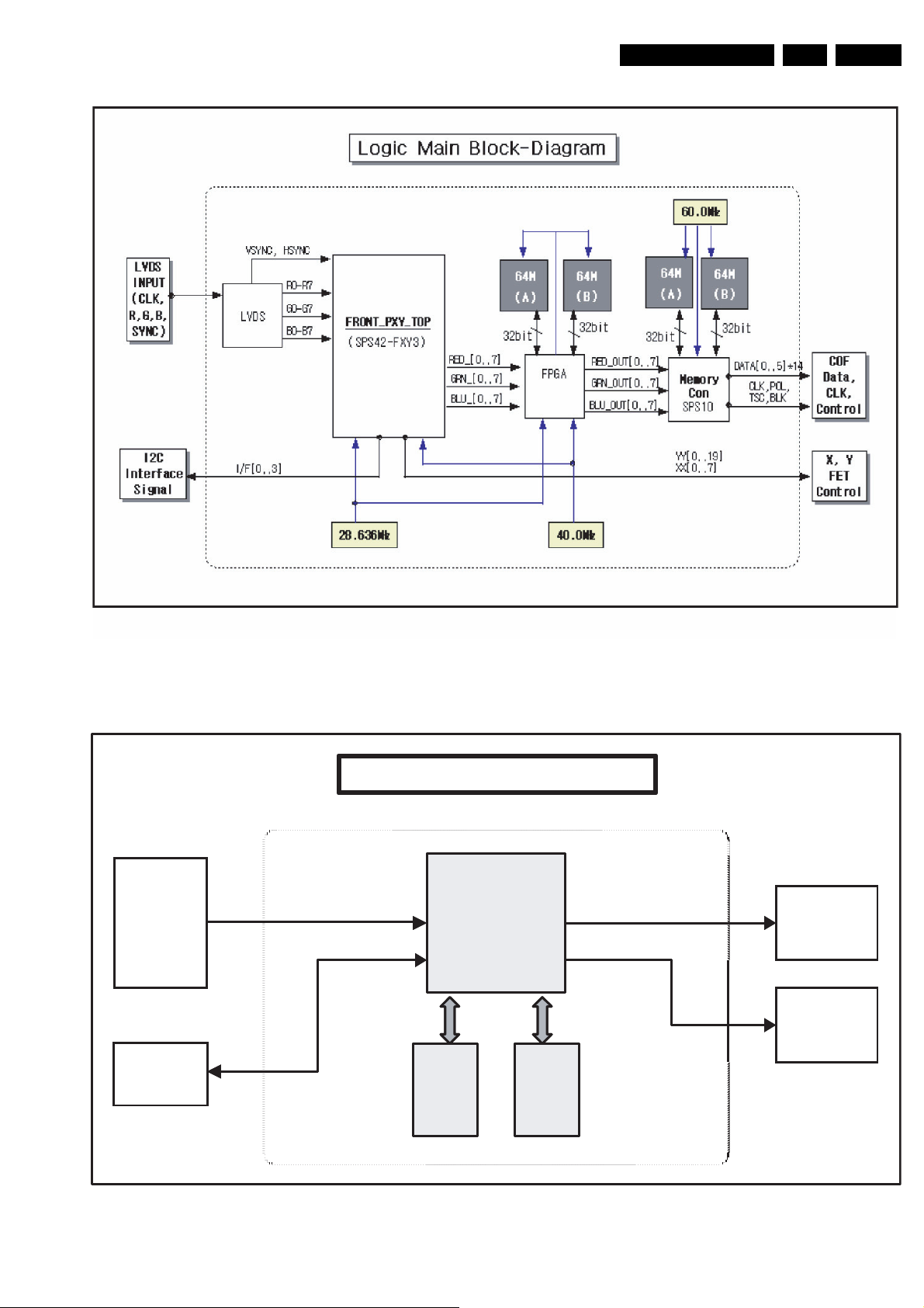
6.1 Block Diagram for Logic Circuit
Figure 6-1 Block diagram (37" SD v4)
Figure 6-2 Block diagram (42" SD v2)
Page 41
Block Diagrams, Test Point Overview, and Waveforms
F_14991_032.eps
030805
F_14991_002.eps
180705
ASIC
SPS - S101
128K
DDR
128K
DDR
ASIC
SPS - S101
128K
DDR
128K
DDR
LVDS
INPUT
(Clock,
RGB,Data,
V-, H-sync,
DE)
I2C
Interface
signal
X, Y
FET
Control
TCP
CLK, DATA
Control
Logic Main Block Diagram
EN 41SDI PDP 6.
Figure 6-3 Block diagram (42" SD v3)
Figure 6-4 Block diagram (42" SD v4)
Page 42
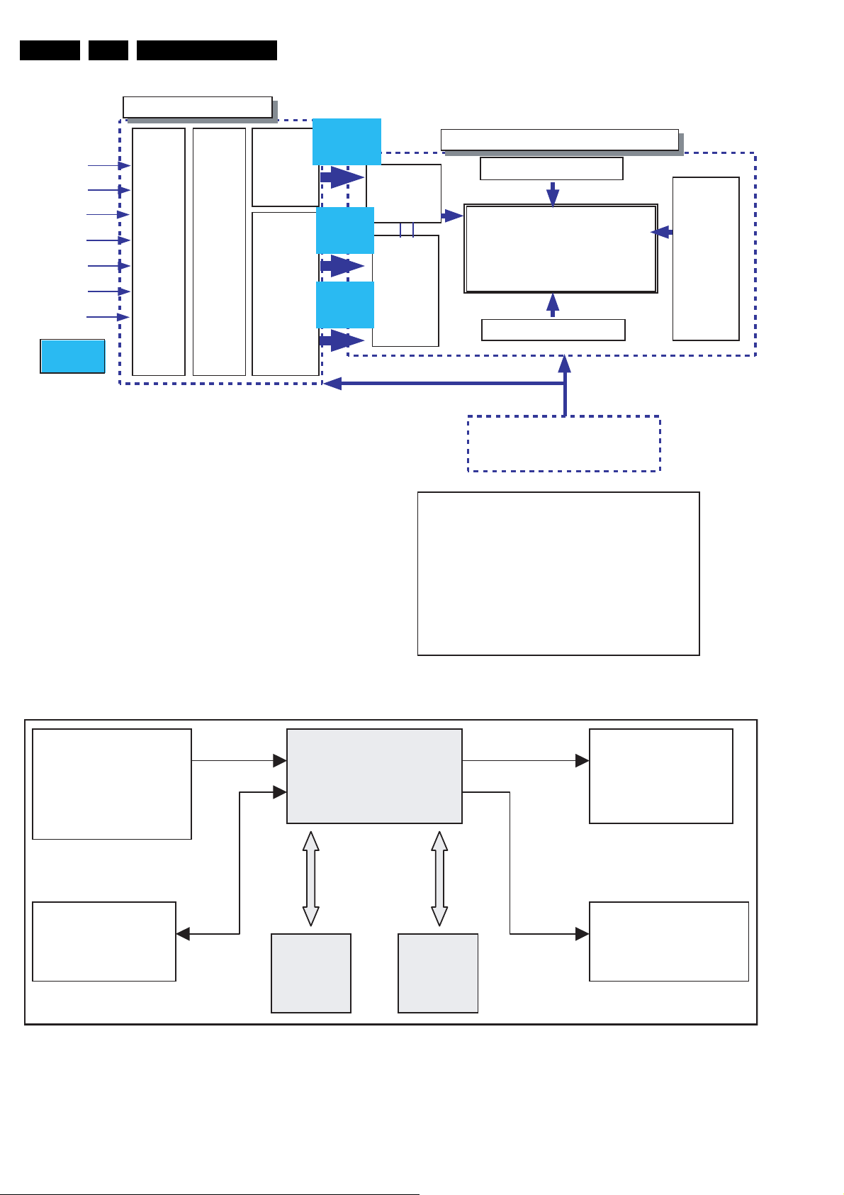
EN 42 SDI PDP6.
1024× 768 Pixels
1024× 3× 768 Cells
YPulse
Generator
Row
Driver
VsVa
Vcc
Vsync
Enable
Hsync
DCLK
DRAM
Display
Data
Driver
Timing Controller
Driver
Timing
Sca n
Timing
Vdd
DATA_R
8Bits
Column Driver
LOGIC CONTROL
DRIVER CIRCUIT & PANEL
DATA_G
8Bits
DATA_B
8Bits
Input Data Processor
Data Controller
XPulse
Generator
Vset Vsc
Ve
LVDS
Interface
Column Driver
- Vcc : Voltage for Logic Control
- Vdd : Voltage for Fet driver
- Va : Voltage for address pulse
- Vs : Voltage sustain pulse
- Vsc : Voltage for scan pulse
- Ve : Voltage for X ramp pulse
- Vset : Voltage for Y ramp pulse
Reference
F_14991_018.eps
030805
ASIC
SPS-NIRB_ 816P
LVDS Input
(DCLK, RG B data,
V/Hsync
X,Y main
Control
128M
DDR
128M
DDR
TCP
CLK, Data control
I2C Interface
Signal
Block Diagrams, Test Point Overview, and Waveforms
Figure 6-5 Block diagram (42" HD v3)
Figure 6-6 Block diagram (42" HD v4)
Page 43
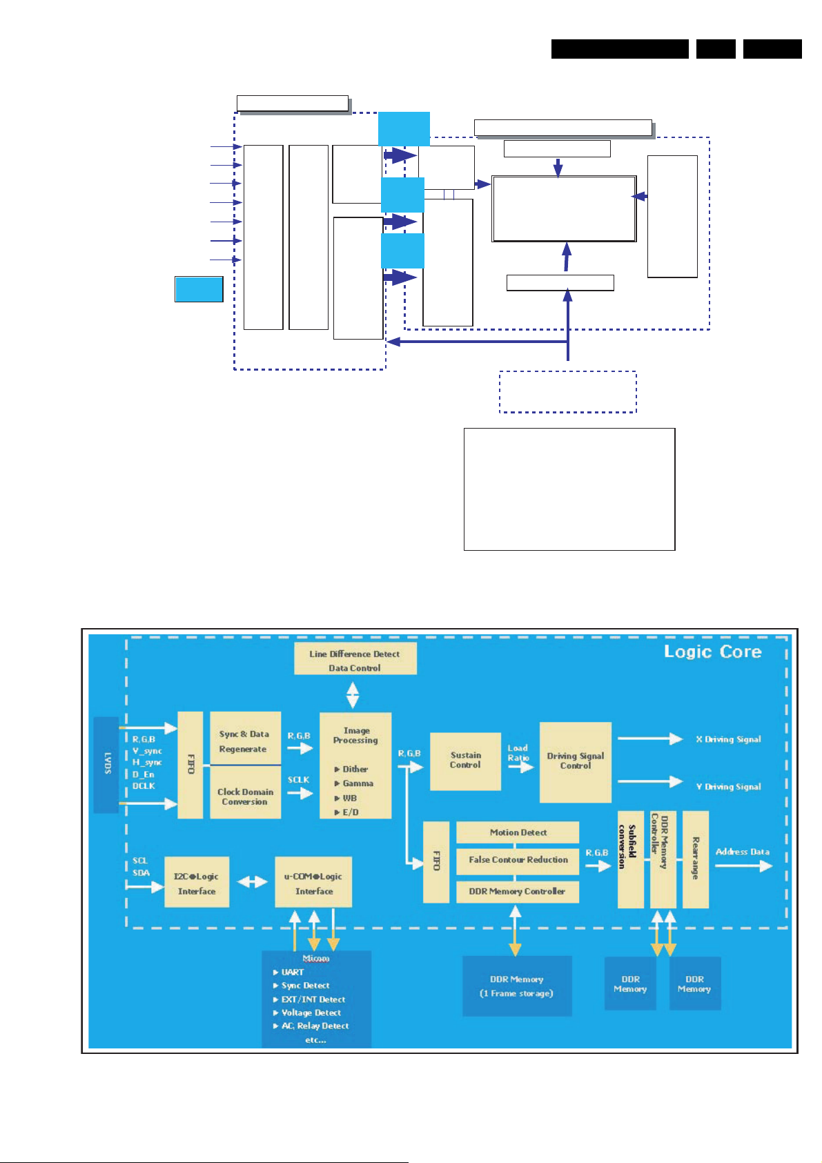
Block Diagrams, Test Point Overview, and Waveforms
- Vcc : Voltage for Logic Control
- Vdd : Voltage for FET driver
- Va : Voltage for address pulse
- Vsc_l
: Voltage sustain low
- Vscan : Voltage for scan high
- Vb : Voltage for X bias
- Vset : Voltage for Y ramp pulse
Reference
136 6× 76 8 Pixels
1366× 3× 768 Cells
YPulse
Generato r
Row
Driv er
Vsync
Enable
Hsync
DCLK
DRAM
Display
Data
Driv er
Timing Controller
Driver
Timing
Sca n
Timing
VsVaVcc Vdd
DATA_R
8(9 )B i ts
Column Driver
LOGIC CONTROL
DRIVER CIRCUIT & PANEL
DATA_G
8(9 )B i ts
DATA_B
8(9 )B i ts
Input Data Processor
Data Con troller
XPulse
Generato r
Vset
Vscan
Vb
LVDS
Interface
Column Driver
Vsc_l
EN 43SDI PDP 6.
Figure 6-7 Block diagram (50" HD v3)
Figure 6-8 Block diagram (50" HD v4)
F_14991_019.eps
030805
Page 44
EN 44 SDI PDP6.
VSCAN
VR8002
VSET
VA8008
VE
VA8003
A5SY CODE
LJ44-00084A
CN8006
D5VL
D3V3
GND
STAN D B Y
VS_ON
AC_DET
RELAY
GND
D5VL
GND
GND
D3V3
D3V3
SERIAL NO.
D3V3
VA8007
L D8004
Vedj
Vuo
L D8003
VA8208
+5V2
L D8001
PS-374-PH 20040420 ED05
N AC INPUT L
100-240V ~ 50/60Hz 6.3 A
CN8001
PBA Flev
ABCDEFGH I
123 45678 9
VPFC
VR8001
V5
VR8009
VR8005
VG
CN8002
SX
VS
VS
GND
GND
GND
GND
VE
VG
D5VL
D5VL
VG
GND
Vscan
GND
Vset
GND
GND
VS
VS
SY
CN8003
VA
D5VL
GND
CN8005
BUFFER
CN8004
HIC8003
8V_STBY
GND
+8.8 V
GND
+5.2V
GND
GND
GND
+12V
POWER_OK
5V_Relay
STANDBY
VA
VSCAN
D5VL
V9
VE
VSET
VG
+8.6V
+ 6.2V
+12V
D3V3
GND
AC_DET
DC_PR07
POWER_OK
CN8007
DC_PR07
GND
GND
GND
GND
GND
THEM_SEN
+5V2
PIRO
PIRO
PFC_OK
+6V2
VA
VR8004
VR8006
D5VL
CN8008
DC_VCC
0V
0V
VPFC
VPFC
0V
HOT(LIVE)
IN-2
IN-3
K
A
K
A
K
A
HIC8002
HIC8001
6.2 PSU Board diagram
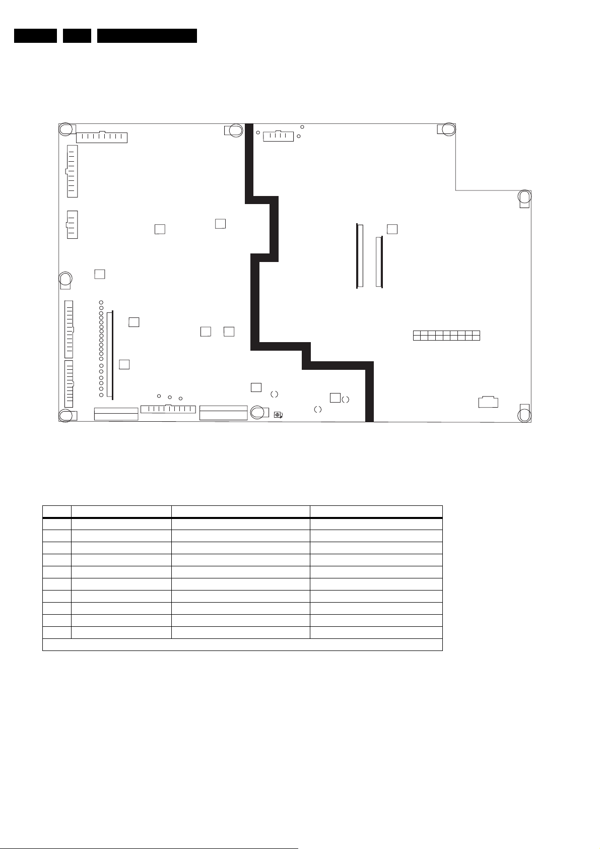
6.2.1 PSU 37" SD v4
Block Diagrams, Test Point Overview, and Waveforms
Figure 6-9 PSU layout
Table 6-1 Adjustment voltage level overview
No Output voltage (V) Voltage Setting (Nominal Load) Output Voltage Variable Point
2 VS 170 V 160 V ~ 185 V
3 VA 70V 60 V ~ 80 V
4 VE 180 V 165 V ~ 195 V
5 VSET 173 V 160 V ~ 180 V
6 VSCAN -160 V -145 V ~ -175 V
7 D5VL 5.2 V 5.0 V ~ 6.0 V
8 D3V3 3.3 V 2.8 V ~ 3.8 V
9 VCC 15 V Fixed
10 5V2 5.4 V 4.5 V ~ 5.6 V
11 9V_Standby 8.5 V ~ 9.5 V Fixed
Check voltage label on the PDP for correct values.
Page 45
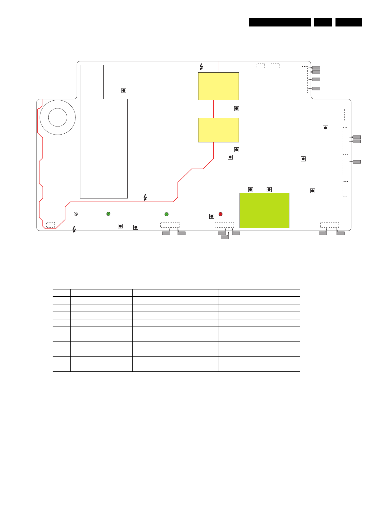
6.2.2 PSU 42" SD v2
CL 36532011_009.eps
050303
COLDHOT
COLD
HOT
13
8004
GREEN
VS
8001
13
8005
13
8006
1510
8009
13413
8002
1812
5
1
5
10
1
4
5
1
1
9
8001
8011
Protection
Board
8010
8008
8003
P7 P6 P2 P1
P4
P5 P3
P12
P13
9
1
2
5
8
8007
P8
P9
P10
P11
P14
GREEN
8002
GREEN
8003
RED
8004
VE
VA
Vcc
VSCAN
VSET
8V6 VFAN
DV5
PFC
3V3_VSB_S
5V_STBY_S
COLD HOT
Block Diagrams, Test Point Overview, and Waveforms
EN 45SDI PDP 6.
Figure 6-10 PSU layout
Table 6-2 Adjustment voltage level overview
No Output voltage (V) Voltage Setting (Nominal Load) Output Voltage Variable Point
1 Vs 87V 78V ~ 92V
2 Va 79V 72V ~ 86V
3 Ve 107V 100V ~ 120V
4 Vset 93V 75V ~ 95V
5 Vscan 79V 65V ~ 85V
6 Vg 15V Fixed
7 D5V 5.2V 5V ~ 5.6V
8 D3V3 3.3V 2.8V ~ 3.7V
Check voltage label on the PDP for correct values.
Page 46
EN 46 SDI PDP6.
VS
VSCAN
GND
VSET
GND
CN8003
VCC
GND
D5VL
VR8004
VS
VR8003
VSET
VR8005
VSCAN
VR8009
D5VL
VR8006
D3V3
VR8007
VA
VR8002
VSB
VR8008
VE
CN8001
AC INPUT
9V_Standby
GND
8V6
GND
5V_SW
GND
12V
GND
POWER OK
5V_Relay Io_2
GND
GND
VA
GND
VA
DC Prot
GND
GND
PIPQ
GND
5V2
GND
Temp Sensor
D3V3
D3V3
GND
GND
D5VL
GND
VS_ON
5V2
CN8009
CN8008
HIC8002
alarm B/D
CN8007CN8004
CN8006
CN8005
HIC8003
VS sub B/D
HIC8001
PFC sub B/D
CN8002
VS
D5VL
VCC
GND
GND
VE
GNDVSGND
PFC
0V
VCC
T-VS
T-VSCAN
T-VCC
T-VSET
T-VA
GND T-3V3
T-5V 9V_Standby 5V2
T-VE
T-VCC-S
T-0V
T-VPFC
T-PFC_VCC
GREEN
GREEN
GREEN
LED8001
LED8002
LED8003
FAIL
RED
LED8004
HOTCOLD
UP
DOWN
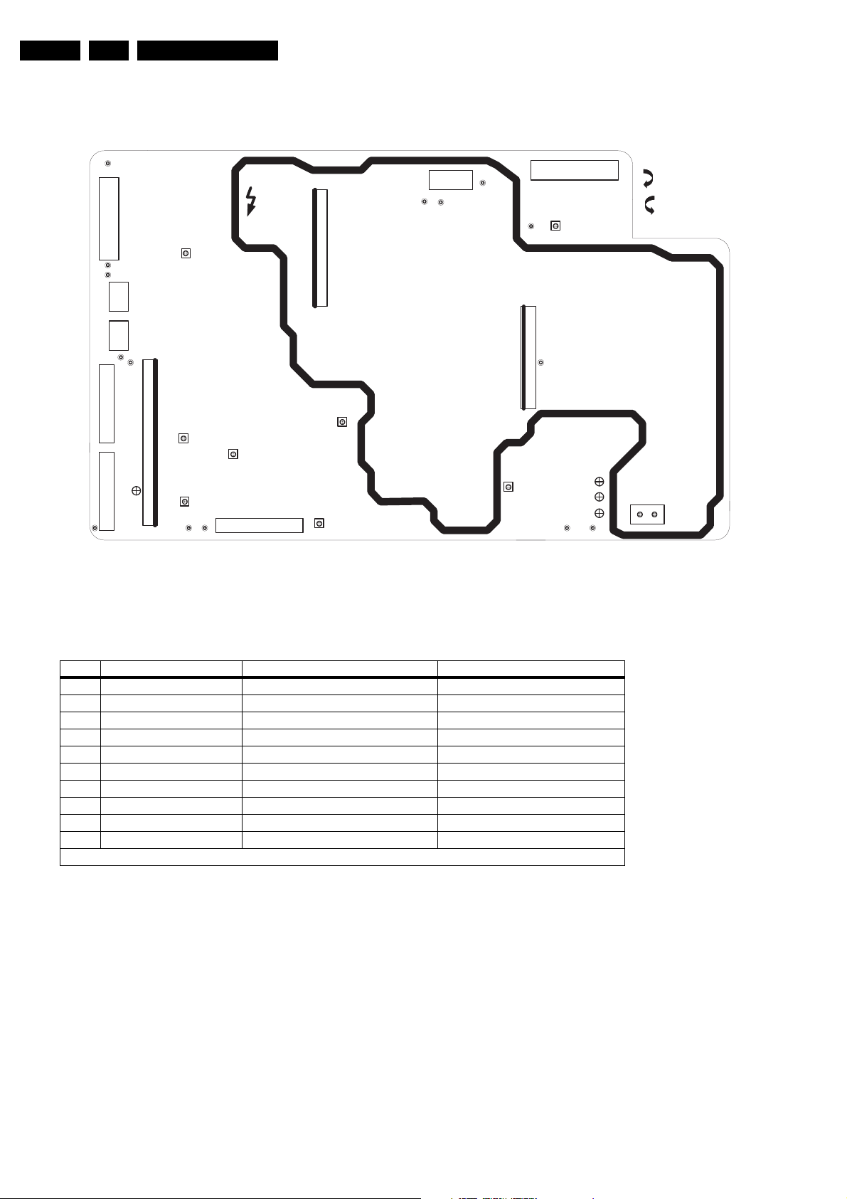
6.2.3 PSU 42" SD v3
Block Diagrams, Test Point Overview, and Waveforms
Figure 6-11 PSU layout
Table 6-3 Adjustment voltage level overview
No Output voltage (V) Voltage Setting (Nominal Load) Output Voltage Variable Point
1 Vs 175V 160V ~ 185V
2 Va 70V 65V ~ 80V
3 Ve 160V 150V ~ 170V
4 Vset 173V 160V ~ 18095V
5 Vscan -60V -55V ~ -75V
6 D5VL 5.2V 4.0V ~ 6V
7D3V3 3.3V 5V ~ 5.6V
8 Vcc 15V Fixed
Check voltage label on the PDP for correct values.
Page 47
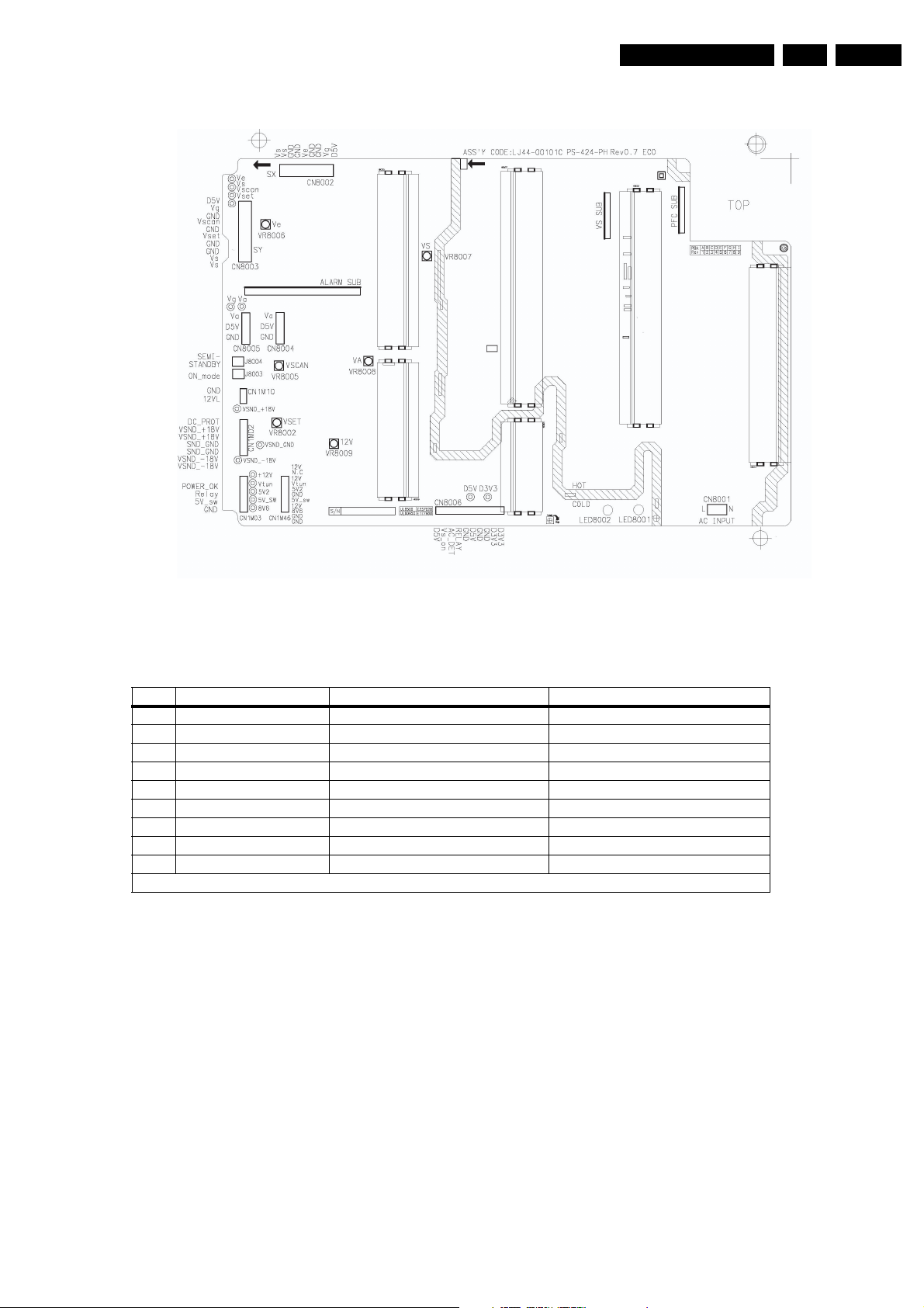
6.2.4 PSU 42" SD v4
F_14991_061.eps
120206
Block Diagrams, Test Point Overview, and Waveforms
EN 47SDI PDP 6.
Figure 6-12 PSU layout
Table 6-4 Adjustment voltage level overview
No Output voltage (V) Voltage Setting (Normal Load) Output Voltage Variable Point
1 VS 207V ± 1% 195V ~ 215V
2 VA 70V ± 1.5% 50V ~ 70V
3 VE 110V ± 1.5% 70V ~ 110V
4 VSET 198V ± 1.5% 180V ~ 210V
5 VSCAN -185V ± 1.5% -170V ~ -190V
6 VSB 5V ± 5% Fixed
7 VG 15V ± 5% Fixed
8 D5VL 5.2V ± 5% Fixed
9 D3V3 3.3V ± 5% Fixed
Check voltage label on the PDP for correct values.
Page 48
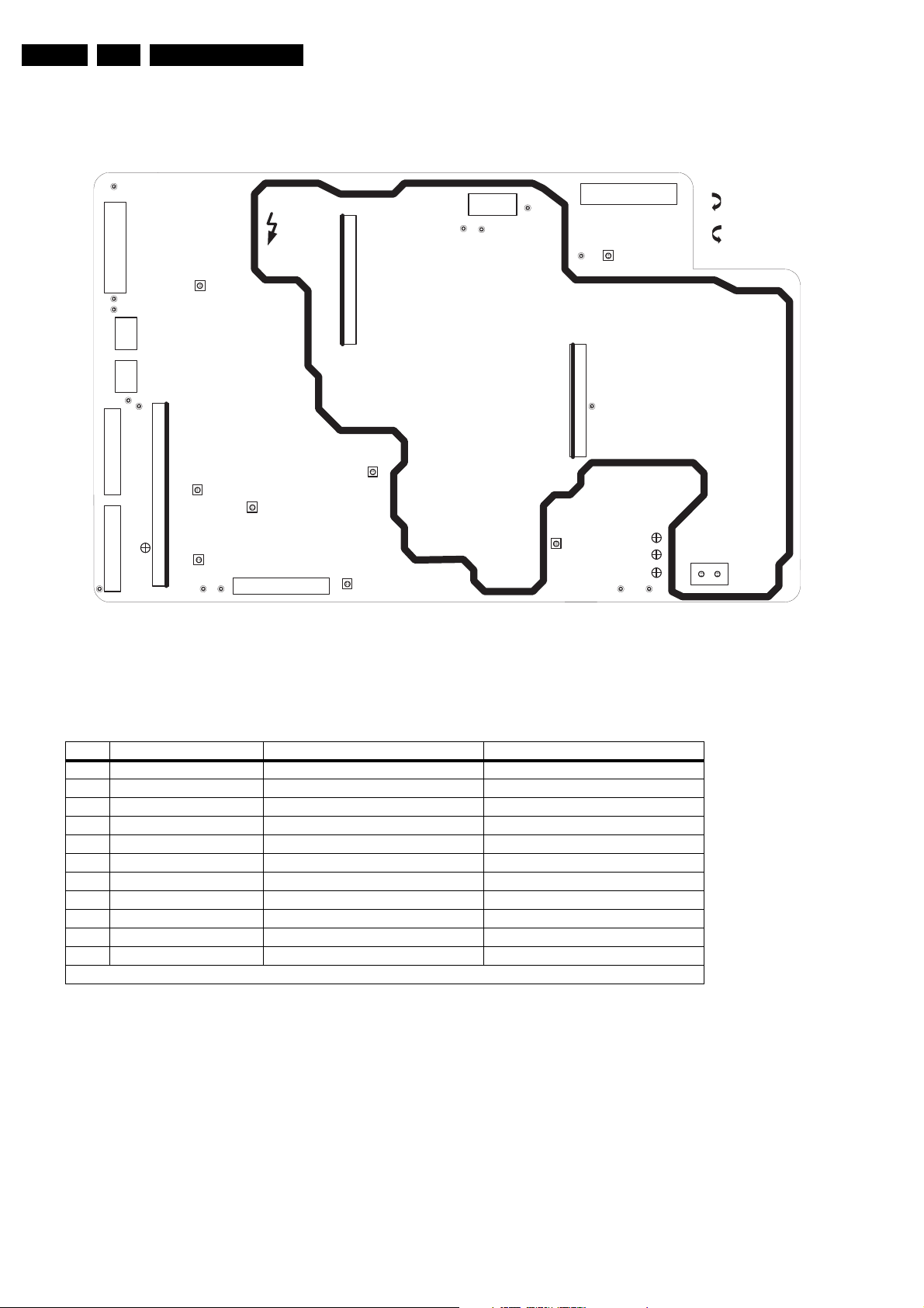
EN 48 SDI PDP6.
VS
VSCAN
GND
VSET
GND
CN8003
VCC
GND
D5VL
VR8004
VS
VR8003
VSET
VR8005
VSCAN
VR8009
D5VL
VR8006
D3V3
VR8007
VA
VR8002
VSB
VR8008
VE
CN8001
AC INPUT
9V_Standby
GND
8V6
GND
5V_SW
GND
12V
GND
POWER OK
5V_Relay Io_2
GND
GND
VA
GND
VA
DC Prot
GND
GND
PIPQ
GND
5V2
GND
Temp Sensor
D3V3
D3V3
GND
GND
D5VL
GND
VS_ON
5V2
CN8009
CN8008
HIC8002
alarm B/D
CN8007CN8004
CN8006
CN8005
HIC8003
VS sub B/D
HIC8001
PFC sub B/D
CN8002
VS
D5VL
VCC
GND
GND
VE
GND
VS
GND
PFC
0V
VCC
T-VS
T-VSCAN
T-VCC
T-VSET
T-VA
GND T-3V3
T-5V 9V_Standby 5V2
T-VE
T-VCC-S
T-0V
T-VPFC
T-PFC_VCC
GREEN
GREEN
GREEN
LED8001
LED8002
LED8003
FAIL
RED
LED8004
HOTCOLD
UP
DOWN
6.2.5 PSU 42" HD v3
Block Diagrams, Test Point Overview, and Waveforms
Figure 6-13 PSU layout
Table 6-5 Adjustment voltage level overview
No Output voltage (V) Voltage Setting (Normal Load) Output Voltage Variable Point
1 PFC 385V ± 2V 370V ~ 400V
2 VS 175V ± 1% 160V ~ 185V
3 VA 70V ± 1% 65V ~ 80V
4 VE 160V ± 2% 150V ~ 170V
5 VSET 173V ± 2% 160V ~ 180V
6 VSCAN -60V ± 2% -55V ~ -75V
7 D5VL 5.2V ± 2% 4.0V ~ 6.0V
8 D3V3 3.3V ± 2% 2.8V ~ 4.0V
9 VCC 15V ± 5% Fixed
10 5V2 5.4V ± 3% 3.5V ~ 6.0V
11 9V_Standby 8.5V ~ 9.5V Fixed
Check voltage label on the PDP for correct values.
Page 49
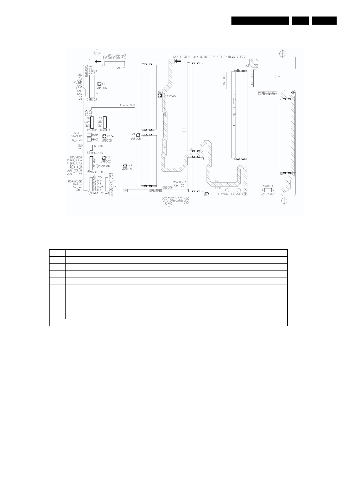
6.2.6 PSU 42" HD v4
F_14991_062.eps
120206
Block Diagrams, Test Point Overview, and Waveforms
EN 49SDI PDP 6.
Figure 6-14 PSU layout
Table 6-6 Adjustment voltage level overview
No Output voltage (V) Voltage Setting (Normal Load) Output Voltage Variable Point
1 Vs 208V 190V ~ 210V
2 Va 70V 50V ~ 70V
3 Ve 90V 80V ~ 105V
4 Vset 195V 180V ~ 205V
5 Vscan -190V -170V ~ -205V
6 Vsb 5V Fixed
7 Vg 15V Fixed
8 D5VL 5.2V Fixed
9 D3V3 3.3V Fixed
Check voltage label on the PDP for correct values.
Page 50
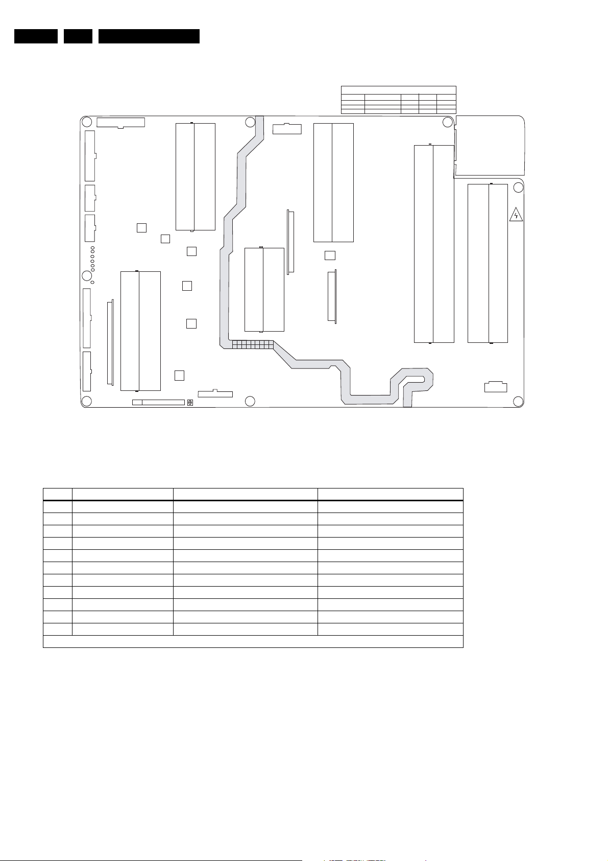
EN 50 SDI PDP6.
VG
VS
VA
VR8005
VR8009
VR8004
SX
SY
CN8002
CN8003
D5VL
V6
GND
GND
GND
GND
V5
V5
V0
V5
V9
GND
GND
GND
GND
GND
GND
GND
GND
D6V
V6
Yscan
Vset
CN8006
VA
VA
VA
VA
BUFFER
1
CN8006
GND
D6V
D3V3
V6
V0
V0
+5V2
IV-2
CN8004
HJC8003
12V
GND
D5V_5W
GND
GND
8V8
+9V_STBY
GND
GND
POWER_OK
+5V_RELAY_IDZ
STAND_BY
1
IV-3
DC_PROT_IN
PIRO
GND
GND
GND
GND
THERMAL_DET
+5V2
1
CN8007
S/N
H8008
VR8007
D3V3
+5VSB
VR8208
VR8006
D5V
Vedj
Vuo
SL
GND
GND
GND
GND
D3V3
D3V3
CN8008
A55V CODE : LJ44-00065A
P5-503-PH
AC INPUT
N
I
L
CN8001
100-240V ~ 50/60Hz BA
WARNING
FOR CONTINUED PROTECTION AGAINST RISK OF FIRE,
REPLACE ONLY WITH SAME TYPE AND RATING OF FUSE.
CAUTION
H8001
TOP
H8002
PCB NAME
VER. NO.
SHEET
FILE NAME
P5-503-PHINZI
00M5510408191
1 OF 6
P5-503-PHINZ1 .PCB
DESIGN
CHECK
APPROVE
00MS5510408191
DIPPING
UL6500:E240806.UL60950:E166582
H8003
HOT (LIVE)
CN8009
DC_VCC
GND
GND
VPFC
IV - 1
COLD (ISOLATED)
H8005
COMP.SILK SCREEN
-P 1/6 -
H8004
PBA Rev HOT (LIVE)
COLD (ISOLATED)
ABCDEFGH
I
123 456779
VR8001
VPFC
HC8001
DONGAH ELECOMM
6.2.7 PSU 50" HD v3
Block Diagrams, Test Point Overview, and Waveforms
Figure 6-15 PSU layout
Table 6-7 Adjustment voltage level overview
No Output voltage (V) Voltage Setting (Normal Load) Output Voltage Variable Point
1 PFC 385V ± 2V 370V ~ 400V
2 VS 175V ± 1% 160V ~ 185V
3 VA 70V ± 1% 65V ~ 80V
4 VE 160V ± 2% 150V ~ 170V
5 VSET 173V ± 2% 160V ~ 180V
6 VSCAN -60V ± 2% -55V ~ -75V
7 D5VL 5.2V ± 2% 4.0V ~ 6.0V
8 D3V3 3.3V ± 2% 2.8V ~ 4.0V
9 VCC 15V ± 5% Fixed
10 5V2 5.4V ± 3% 3.5V ~ 6.0V
11 9V_Standby 8.5V ~ 9.5V Fixed
Check voltage label on the PDP for correct values.
Page 51
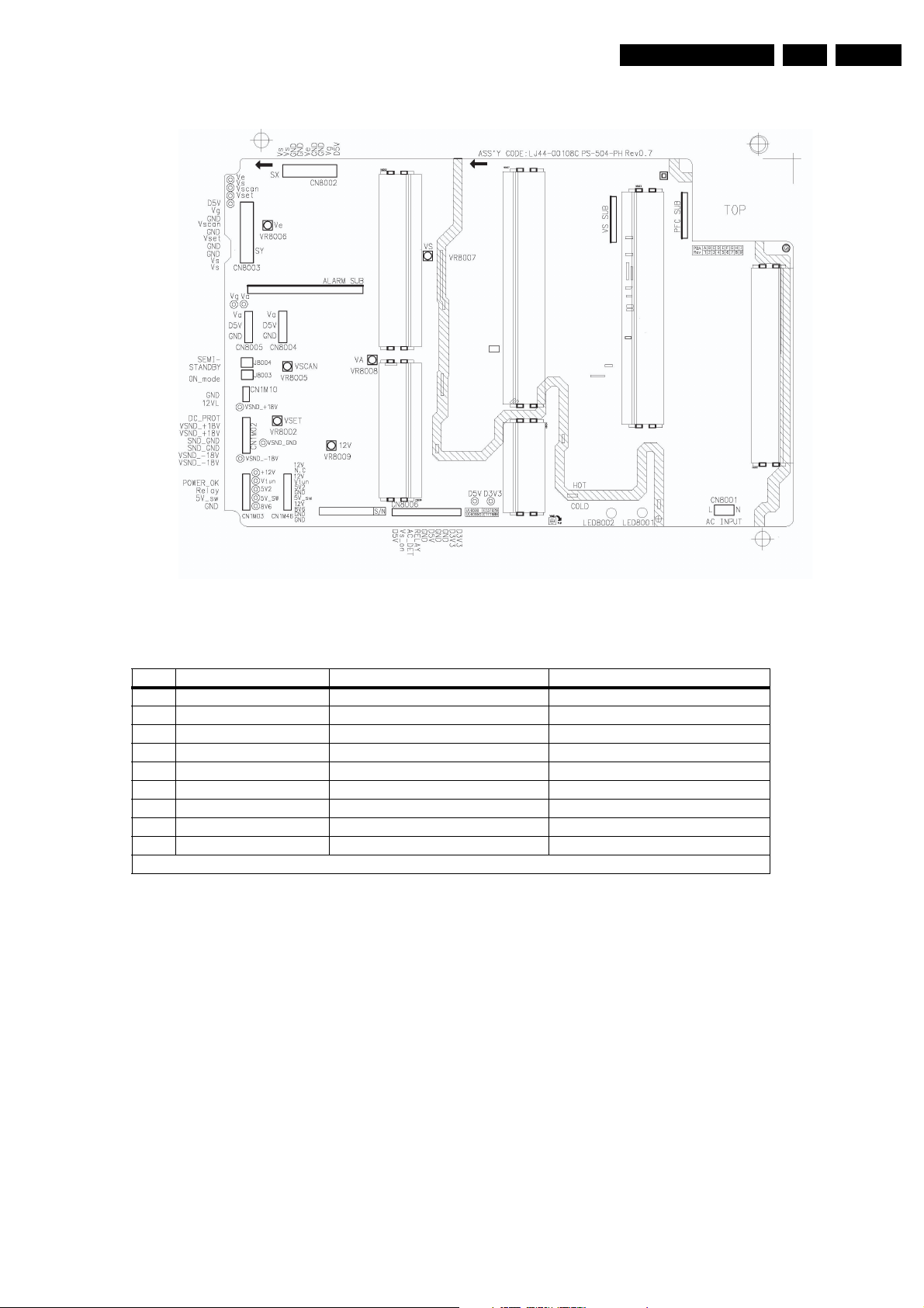
6.2.8 PSU 50" HD v4
F_14991_063.eps
120206
Circuit Diagrams and PWB Layouts
EN 51SDI PDP 7.
Figure 6-16 PSU layout
Table 6-8 Adjustment voltage level overview
No Output voltage (V) Voltage Setting (Normal Load) Output Voltage Variable Point
1 VS 200V ± 1% 195V ~ 215V
2 VA 70V ± 1.5% 50V ~ 70V
3 VE 100V ± 1.5% 70V ~ 110V
4 VSET 195V ± 1.5% 180V ~ 210V
5 VSCAN -175V ± 1.5% -170V ~ -185V
6 VSB 5V ± 5% Fixed
7 VG 15V ± 5% Fixed
8 D5VL 5.2V ± 5% Fixed
9 D3V3 3.3V ± 5% Fixed
Check voltage label on the PDP for correct values.
7. Circuit Diagrams and PWB Layouts
Not applicable.
Page 52
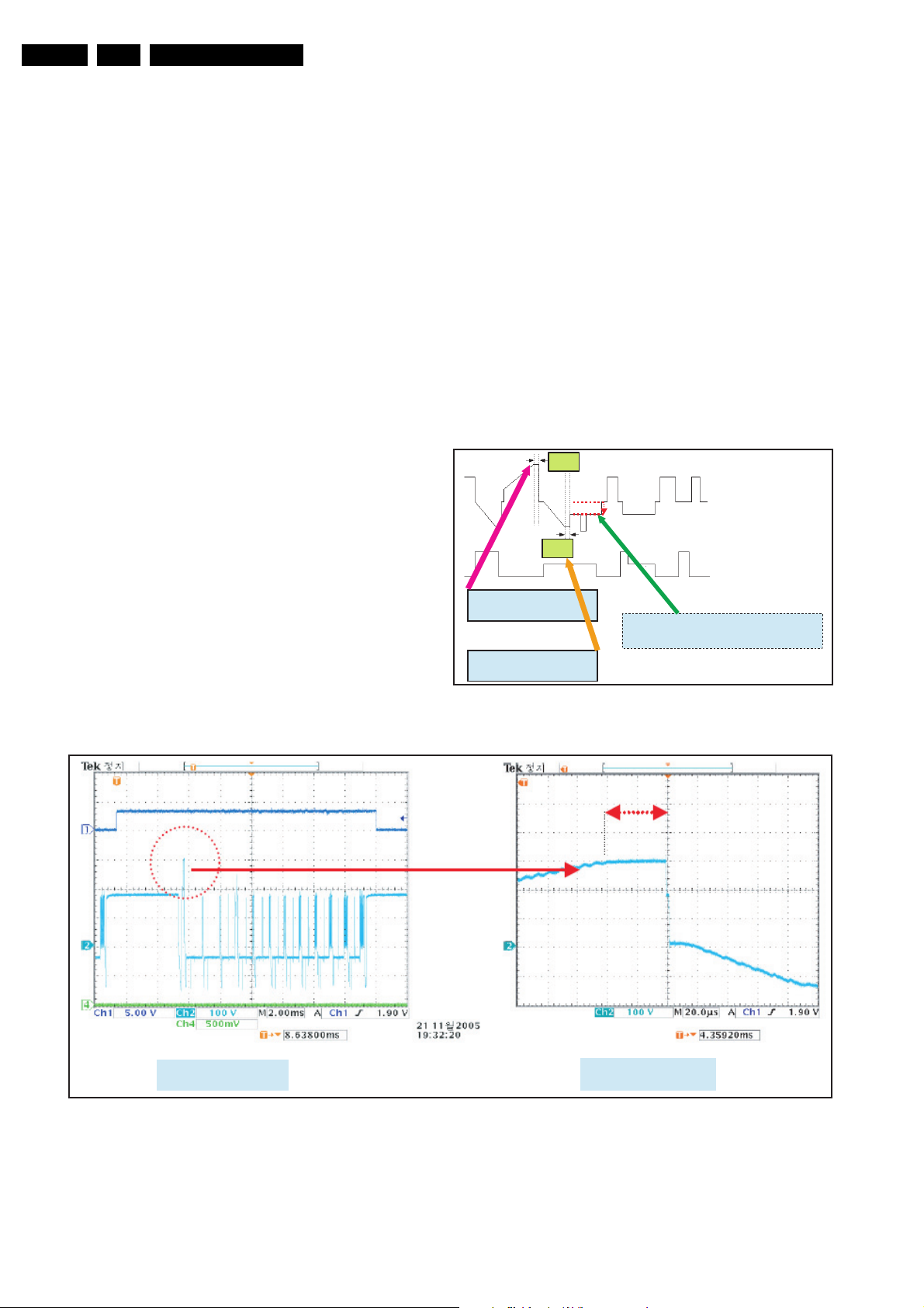
EN 52 SDI PDP8.
G_14992_001.eps
190106
Adjust VR5001 to set the time of
Yrr( Ri sing Ramp) 40
µs
Adjust VR5002 to set the time
of Yfr (Falling Ramp_1st) 16
µs
Adjust VR5000 to set the voltage to -38 V.This
alignment can be executed by using a DMM, the
+ of the DMM on Y-sca n H test point
40 µs
16 µs
Ch2 = 100V/2ms/div
Ch2 = 100V/20µs/div
G_14992_002.eps
190106
8. Alignments
Alignments
Index of this chapter:
8.1 Alignments 37" SD v4
8.2 Alignments 42" SD v2
8.3 Alignments 42" SD v3
8.4 Alignments 42" HD v3
8.6 Alignments 42" HD v4
8.7 Alignments 50" HD v3
8.8 Alignments 50" HD v4
8.9 Alignment value overview (all screens)
Note:
• Figures can deviate due to the different model executions.
Important: Remove all non-default jumpers and reset all DIP
switches, after the repair!
8.1 Alignments 37" SD v4
1. Set the pattern to Full White (place jumper CN2008 on the
Logic Board).
2. Set Vsch (see Figure “Test point location LJ92-0102A”) to
-38V (see Figure “Waveform adjustment (Y-Board)”).
Check with a digital multimeter, connected between the Yscan test point and ground. Adjust the voltage with
VR5000.
3. Check the waveform using an Oscilloscope.
• Triggering through V_TOGG of the LOGIC Board (see
Figure “Logic PWB”).
• Connect the “ODD” test point, located at the centre of
Y_buffer (see Figure “Potentiometer locations LJ9201149A”), to the other channel, and then check the first
Subfield waveform of one TV-Field.
• Check the waveform by adjusting Horizontal Division of
the oscilloscope.
4. Adjust the flat time of the rising ramp of the 1st subframe to
40 µS with VR5001 (see Figure “Rising ramp flat time
adjustment”).
5. Adjust the flat time of the falling ramp of the 1st subframe
to 16 µs with VR5002 (see Figure “Falling ramp flat time
adjustment”).
• This is a difficult adjustment.
• It is easier and more accurate to do the following:
– Count 3 pulses between A and B;
– Set the difference between A and B to 40 V; the
time between C and D will then automatically be
set to approximately 16 µS
– Settings of the oscilloscope: vertically 20VDC/div,
horizontally 10 µS/div.
6. Check with the oscilloscope if the voltage of Vsch is -38 V
(see Figure “Y-scan H waveform”).
Special notice: It is very important, that you execute this
adjustment on the 1st Sub-Field (SF) of the 1st Frame of the
Reset waveform and then move to the 3rd Sub-field for
adjusting.
Figure 8-1 Waveform adjustment (Y-Board)
Figure 8-2 Rising ramp flat time adjustment (Y-Board)
Page 53
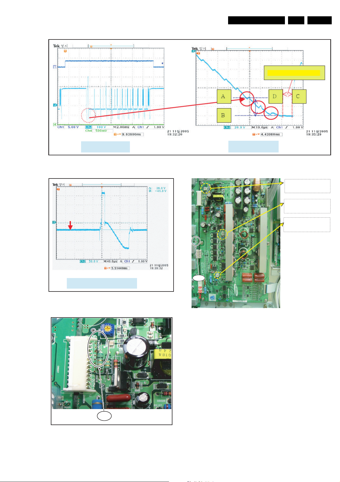
Alignments
Ch2 = 100V/2ms/div
Ch2 = 20V/10µs/div
G_14992_003.eps
190106
Not easy to set to 16 µs
G_14993_001.eps
240306
1
Vsch
1. VR5000 Adjustment:
2. VR5001 Adjustment:
3. VR5002 Adjustment:
Falling ramp flat time: 16 us
Rising ramp flat time: 40 us
Vsch TP: 38 V
F_14991_051.eps
240306
1
TP_ODD
Figure 8-3 Falling ramp flat time adjustment (Y-Board)
EN 53SDI PDP 8.
Ch2 = 40us/50V/DC/div
G_14992_004.eps
Figure 8-4 Y-scan H waveform (Y-Board)
Figure 8-5 Test point location LJ92-01021A
190106
Figure 8-6 Potentiometer locations LJ92-01149A
Page 54
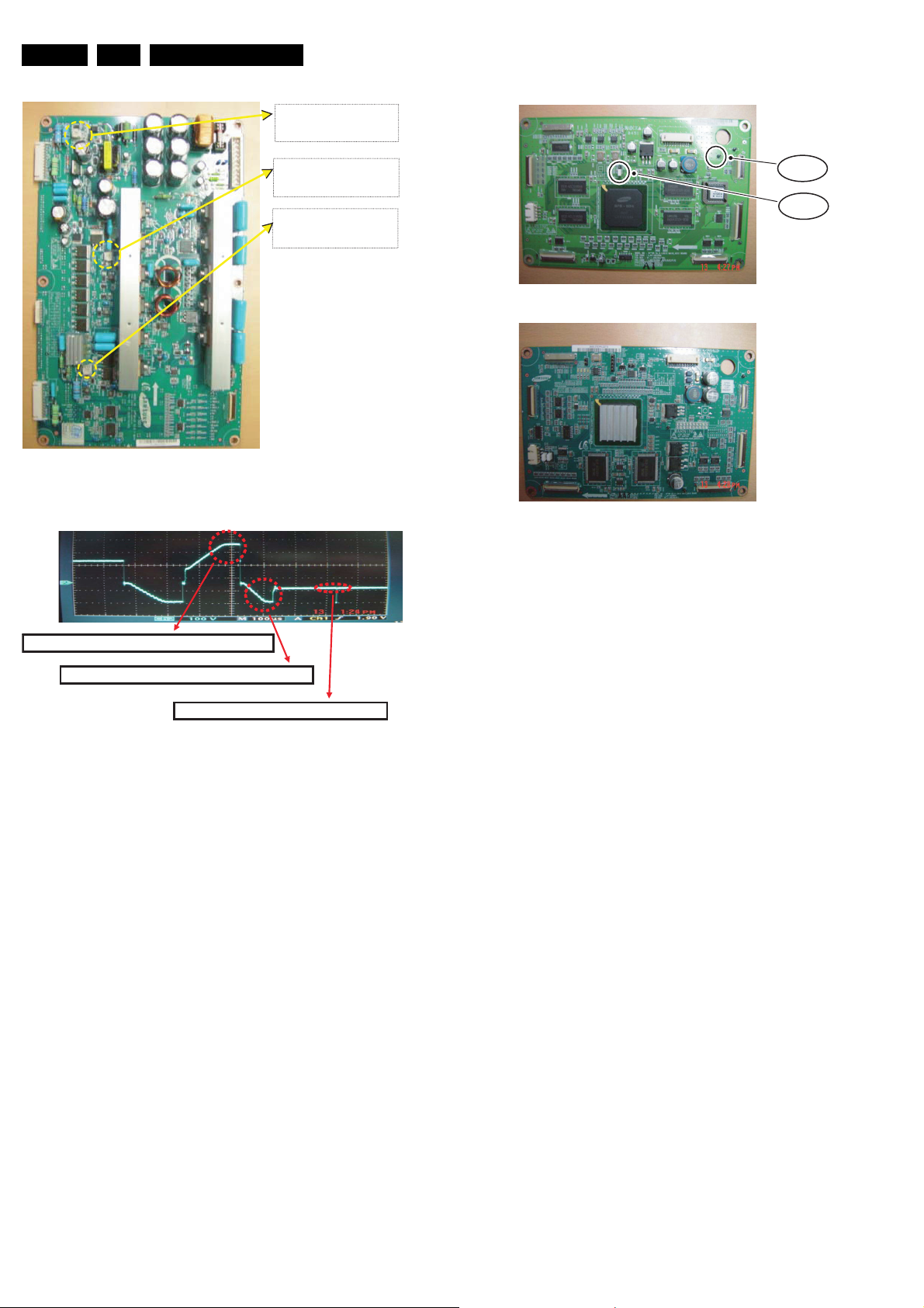
EN 54 SDI PDP8.
1. VR5000 Adjustment:
2. VR5001 Adjustment:
3. VR5002 Adjustment:
Falling ramp flat time: 16 us
Rising ramp flat time: 40 us
Vsch TP: 38 V
F_14991_067.eps
140206
GXWW\y}GhGGGWZGPyGyOGG ༕
GYWW\y}GhGGG]XGPyGmOGG
༕
GWWW\y}GhGG}GG}G – }_Z
G_14991_066.eps
140206
sq`
Y
TWXW\^
h
sq`YTWX
W
\
]h
Figure 8-7 Potentiometer locations LJ92-01149B
Alignments
GVGsq`YTWXX[\h
V_TOGG
1
1
CN2008
Figure 8-8 Wave form adjustment (Y-Main board)
s
F_14991_068.eps
Figure 8-9 Logic PWB
230306
Page 55
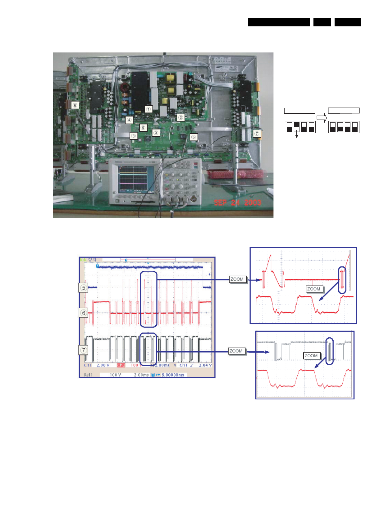
8.2 Alignments 42" SD v2
1) Preparation
1
Insert jumper J8002 on PSU board
2 Connect the Jig connector switch
3
Put the Logic board dipswitches
into internal mode, to generate
a Full White screen
External Mode
Internal Mode
1234 1234
4 Connect the AC power jig
Connect the Oscilloscope:
5 CH1: V-SYNC (CN201)
6 CH2: Y-output (OUT4)
7 CH3: X-output (TP OUT )
8 Connect the Key-scan Board
2) Turn-On.
- Turn on the Power switch
- Check the LED on the Logic Board
- Check waveform of X- and Y-board
(Refer to Picture below)
Vsync
Y-Output
X-Output
Alignments
EN 55SDI PDP 8.
Figure 8-10 Adjusting procedure (42" SD v2)
Figure 8-11 Waveform of X- and Y-board (42" SD v2)
Page 56
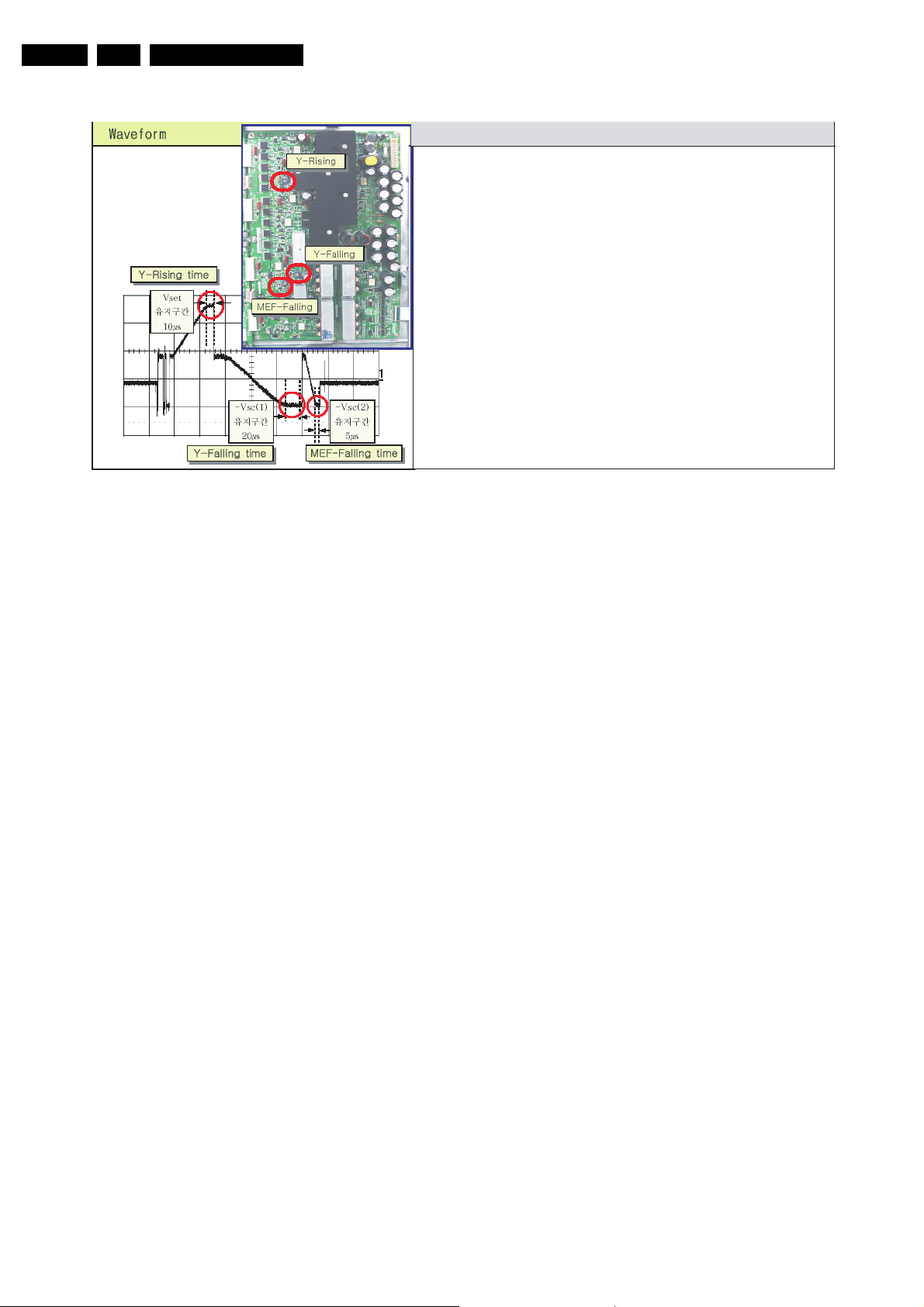
EN 56 SDI PDP8.
1) Make Full White on Screen.
2) Observe waveform using Oscilloscope.
a Check OUT4 TP in Y-buffer(upper).
Observe the waveform of the third waveform of 1TV-Field.
b Adjust the division of oscilloscope like the left picture
c Adjust the period of Vset as 10µS, that of -Vsc(1) as 20µs,
that of -Vsc(2) as 5µs, turning VR (Variable Resistor)
(only,when you adjust each period of -Vsc(1) & -Vsc(2)
adjust Vertical Division of oscilloscope as '2V or 5V')
d VR for Vset : VR5003 (Y_main)
VR for -Vsc(1) : VR5001 (Y_main)
VR for -Vsc(2) : VR5002 (Y_main)
Procedure
Alignments
Figure 8-12 How to adjust the waveform (42" SD v2)
Page 57
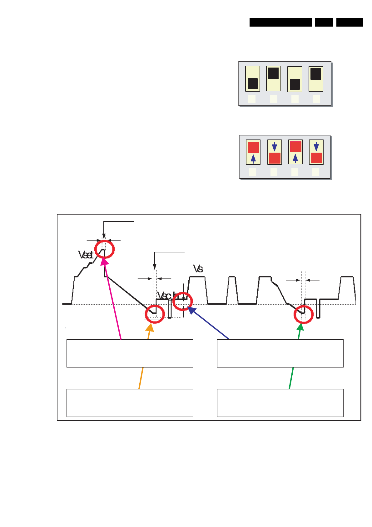
Alignments
1 2 3 4
1
2
3
4
EN 57SDI PDP 8.
8.3 Alignments 42" SD v3
1. Put the dipswitches on the Logic Board in the internal
position to get a Full White Pattern.
2. You can find the location of the test point and
potentiometers in Figure “Potentiometer locations”.
3. Adjust Vsch to 40 V with VR5004.
4. Check the waveform with an Oscilloscope.
• Take the trigger signal from the testpoint marked “V-
sync” on the Logic Board.
• Connect the testpoint marked “OUT 4”, located in the
centre of Y_buffer Board to the other channel, and then
check the first Subfield operating waveform of one TVField.
• Check the waveform again after adjusting Horizontal
Division. Check the Reset waveform when the
V_TOGG Level is changed.
• Set the Vset to 10µs by adjusting VR5002.
• Set the Falling maintenance time to 30 µs by adjusting
VR5003.
• Change the waveform position of Oscilloscope to the
3rd Subfield and then set the Falling maintenance time
to 30µsby adjusting the VR5001. GND maintenance
section should be checked after the Vertical Division is
readjusted to “2 V or 5 V”.
Special notice: It is very important, that you execute this
adjustment on the 1st Sub-Field (SF) of the 1st Frame of the
Reset waveform and then move to the 3rd Sub-field for
adjusting.
Figure 8-13 DIP switch mode: External
Figure 8-14 DIP switch mode: Internal
rising maintenance time
falling maintenance time
Adjust VR5002 to set the time of
Yrr (Rising Ramp) 10
µs
Adjust VR5004 to set the voltage of
Vsch (Scan high voltage) 40 V
Adjust VR5003 to set the time of
Yfr (Falling Ramp_1st) 30
µs
Adjust VR5001 to set the time of
Yfr (Falling Ramp_3rd) 30
µs
Figure 8-15 TCP ramp waveform inclination adjustment (Y-Board)
Page 58
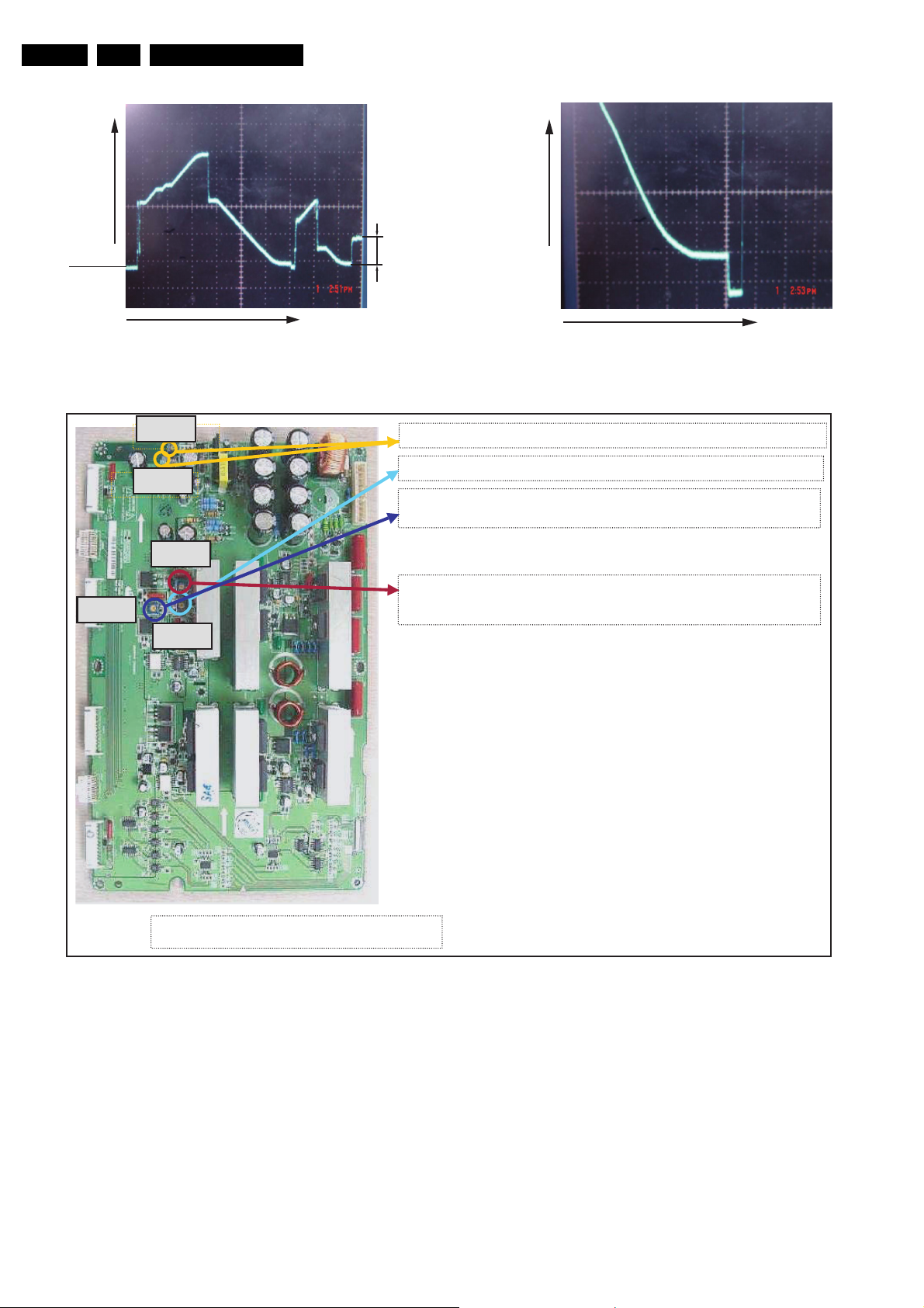
EN 58 SDI PDP8.
(V)
20V/div.
50ms/div.
(t)
4. VR5001 Adjustment: 3rd SF Falling Ramp flat time => Typ. 30 µsec
* Pay close attention to above adjustment
1. VR5004 Adjustment: Vsch TP => 40 volt
2. VR5002 Adjustment: Rising Ramp flat time: Typ. 10 µsec
3. VR5003 Adjustment: Falling Ramp flat time => Typ. 30 µsec
VR5003
VR5002
VR5001
VR5004
TP:Vsch
(V)
50V/div.
DC=0V
Alignments
40V
20ms/div.
(t)
Figure 8-16 Rising ramp
Figure 8-17 Falling ramp
Figure 8-18 Potentiometer locations
Page 59
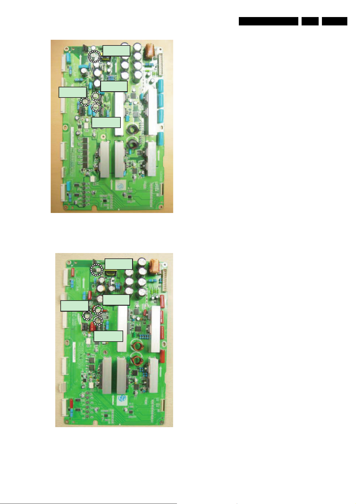
Alignments
G[WW\y}
GZWW\y}
XWW\y}
GYWW\y}
sq`YTWXY_[h
F_14991_070.eps
140206
G[WW\y}
GZWW
\y}
XW
W\y}
GYWW\y}
sq`YTW
W`[[i
F_14991_069.eps
140206
EN 59SDI PDP 8.
Figure 8-19 Potentiometer locations LJ92-01284A
Figure 8-20 Potentiometer locations LJ92-00944B
Page 60
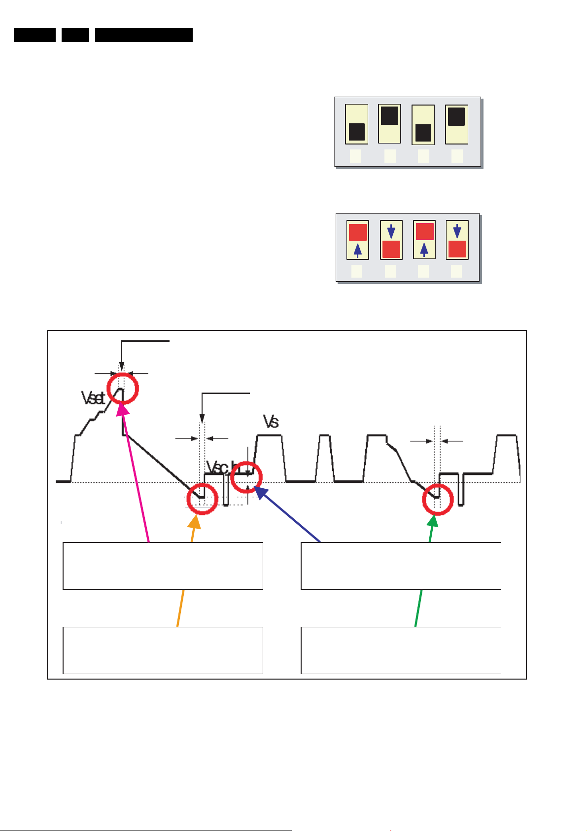
EN 60 SDI PDP8.
1 2 3 4
1
2
3
4
Adjust VR5003 to set the time of
Yfr (Falling Ramp_1st) 20
µs
Adjust VR5002 to set the time of
Yrr (Rising Ramp) 20
µs
Adjust VR5001 to set the time of
Yfr (Falling Ramp_3rd) 10
µs
Adjust VR5004 to set the voltage of
Vsch (Scan high voltage) 40 V
rising maintenance time
falling maintenance time
Alignments
8.4 Alignments 42" HD v3
1. Put the dipswitches on the Logic Board in the internal
position to get a Full White Pattern.
2. Adjust Vsch to Clock-wise max by using VR5004 (Vsch
should be connected to "+" unit of DMM).
3. Check the waveform using Oscilloscope.
• Triggering through V_TOGG of LOGIC Board.
• Connect the OUT 4 Test Point at the centre of Y_buffer
to other channel, and then check the first Subfield
operating waveform of one TV-Field.
• Check the waveform again after adjusting Horizontal
Division. Check the Reset waveform when the
V_TOGG Level is changed.
• Set the Vset to 20 µs by adjusting VR5002. GND
maintenance section should be checked after the
Vertical Division is readjusted to “2 V or 5 V”.
• Set the Falling maintenance time to 20 µs by adjusting
VR5006.
• Change the waveform position of Oscilloscope to the
3rd Subfield and then set the Falling maintenance time
to 10µs by adjusting the VR5003. GND maintenance
section should be checked after the Vertical Division is
readjusted to “2 V or 5 V”.
Special notice: It is very important, that you execute this
adjustment on the 1st Sub-Field (SF) of the 1st Frame of the
Reset waveform and then move to the 3rd Sub-field for
adjusting.
Figure 8-21 DIP switch mode: External
Figure 8-22 DIP switch mode: Internal
Figure 8-23 TCP ramp waveform inclination adjustment (Y-Board)
Page 61
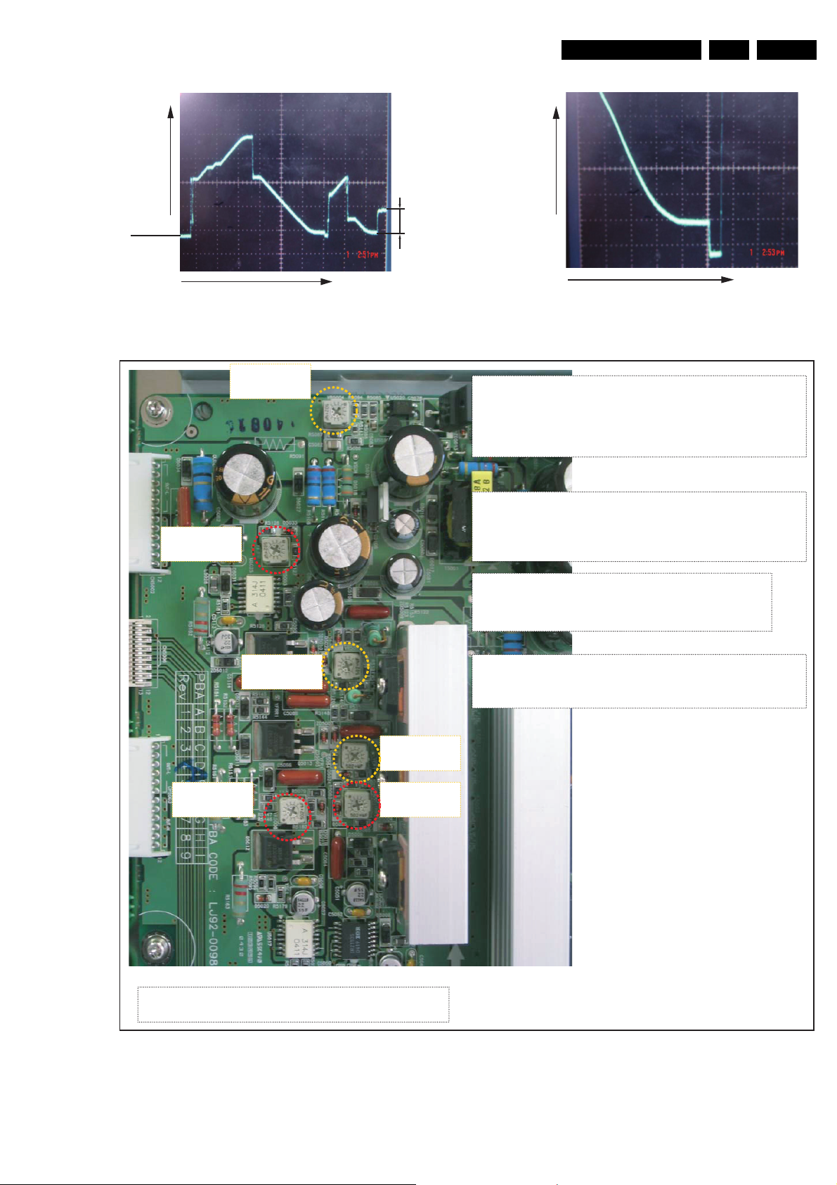
Alignments
(V)
50V/div.
DC=0V
20ms/div.
(t)
40V
(V)
20V/div.
50ms/div.
(t)
* Pay close attention to above adjustment
1. VR5004 / Adjustment; Clock-wise to max
2. VR5005/ Adiustment; Clock-wise to max
3. VR5001/ Adiustment; Clock-wise to 4
th
division
4. VR5002 Adjustment: Rising Ramp flat time:
=> Typ. 20usec
6. VR5003 Adjustment: 3th SF Falling Ramp flat time
=> Typ. 10usec
5. VR5006 Adjustment: Falling Ramp flat time
=> Typ. 20usec
VR5004
VR5005
VR5001
VR5003
VR5002VR5006
EN 61SDI PDP 8.
Figure 8-24 Rising ramp
Figure 8-25 Falling ramp
Figure 8-26 Potentiometer locations
Page 62
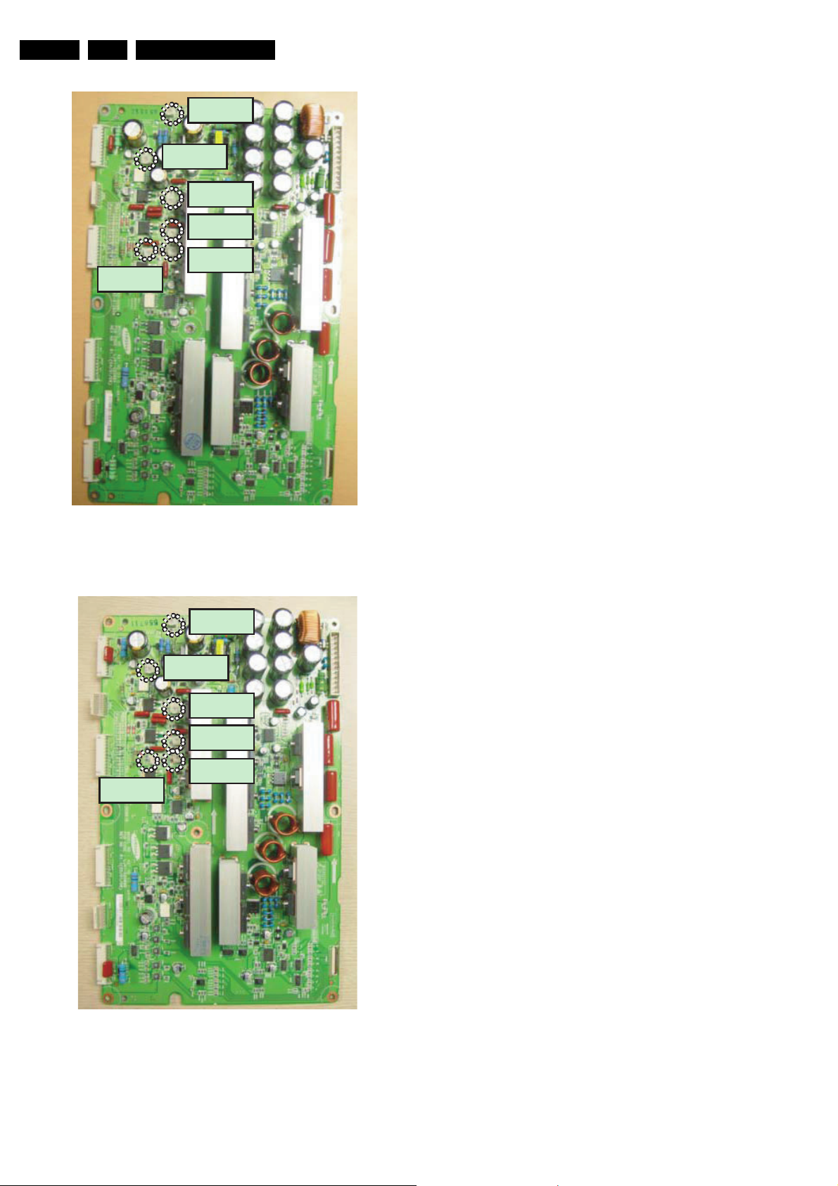
EN 62 SDI PDP8.
G[WW\y}
GZWW
\y}
GXWW\y}
G\WW\y}
GYWW\y}
G]WW
\y}
sq`YTW
W`_Xh
F_14991_071.eps
140206
G[WW\y}
GZWW\y}
GXWW\y}
G\WW\y}
GYWW\y}
G]WW\y}
sq`YTWW`_Xi
F_14991_072.eps
140206
Alignments
Figure 8-27 Potentiometer locations LJ92-00981A
Figure 8-28 Potentiometer locations LJ92-00981B
Page 63
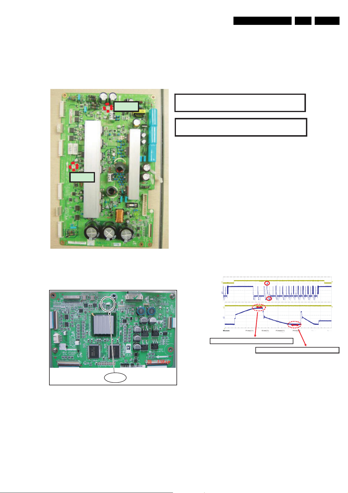
Alignments
GZWW\y}
GXWW\y}
GXWW\y}UXhGaGyGGyGGa
GW] ༕
GZWW\y}UYhGaGmGy GGaG
GW_ ༕
sq`YTWXZZ^h
F_14991_074.eps
140206
G_14993_002.eps
270306
1
CN2034
EN 63SDI PDP 8.
8.5 Alignments 42" SD v4
1. Get Pattern to be Full White (place jumper CN2034 on
Logic Board).
2. Check the waveform using an Oscilloscope.
• Triggering through V_TOGG of LOGIC Board.
• Connect the OUT 240 Test Point at the centre of
Y_buffer to other channel, and then check the first aidreset waveform from the last sustain of 1TV-Field.
• Check the waveform again after adjusting Horizontal
Division.
Check the Reset waveform when the V_TOGG Level
is changed.
• Adjust the flat time of the rising ramp to 60μs with
VR5001.
• Adjust the flat time of the falling ramp to 80μs with
VR5003.
Figure 8-29 Potentiometer locations
Figure 8-30 Jumper location (Logic board)
hG
GXWW\y}G
Figure 8-31 Wave form adjustment (Y-Main board)
GGW
]GP
yGyOGG ༕
GZWW\
y}GhG
GGW
_GP
yGmOGG ༕
F_14991_073.eps
140206
Page 64
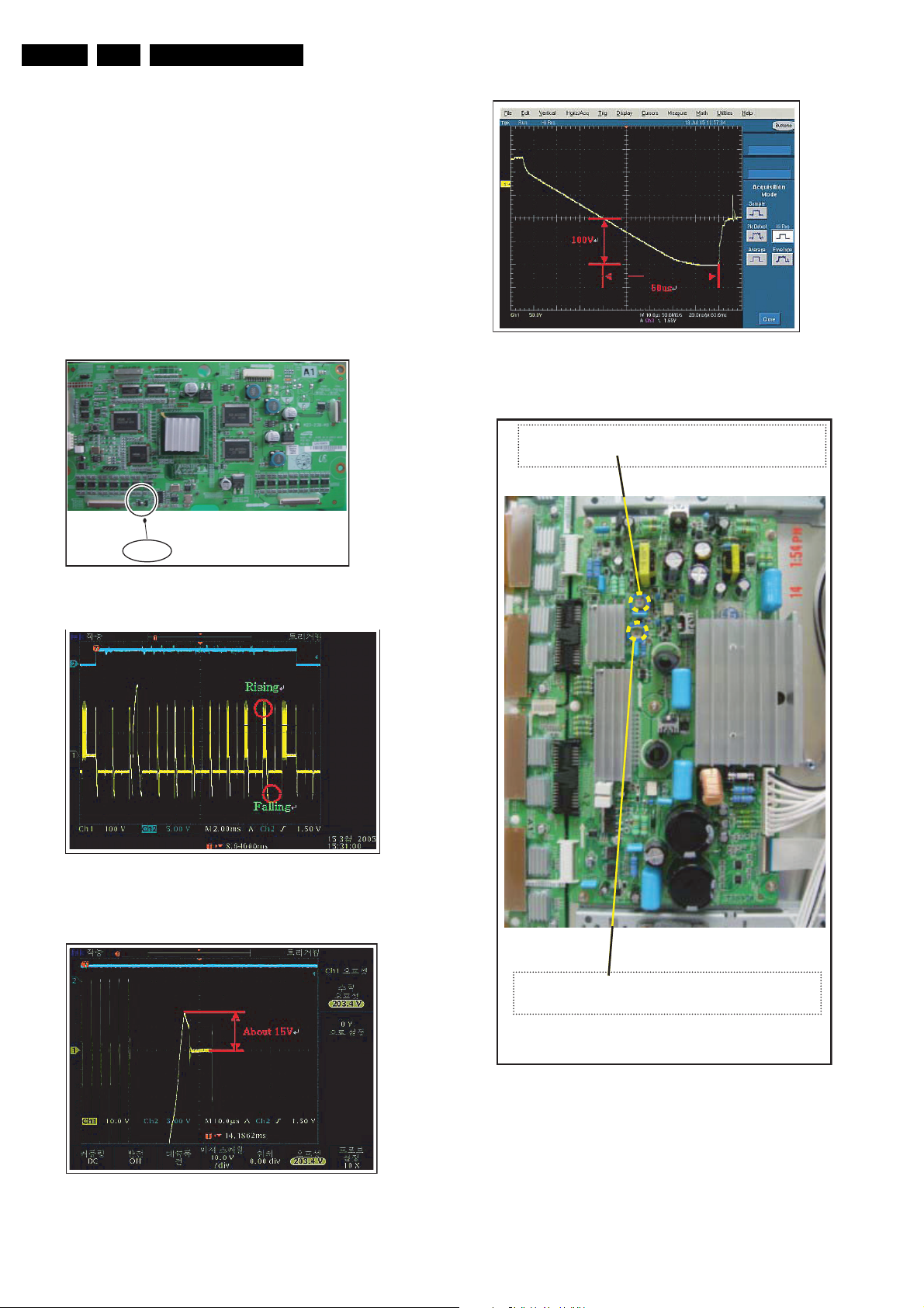
EN 64 SDI PDP8.
G_14993_003.eps
270306
1
CN2072
F_14991_023.eps
030805
F_14991_024.eps
030805
F_14991_025.eps
030805
F_14991_026.eps
160206
VR5002 Adjustment : Falling ramp(Yfr)
VR5001 Adjustment : Risi
LJ92 - 01200A
ng ramp(Yrr)
8.6 Alignments 42" HD v4
1. Get Pattern to be Full White (place jumper CN2072 on
Logic Board).
2. Check the waveform using an Oscilloscope.
• Triggering through V_TOGG of LOGIC Board.
• Connect the OUT 240 Test Point at the centre of
Y_buffer to other channel, and then check the first aidreset waveform from the last sustain of one TV-Field.
• Check the waveform again after adjusting Horizontal
Division.
Check the Reset waveform when the V_TOGG Level
is changed.
• Set the 15V by adjusting VR5002.
• Set the 100V and 50us by adjusting VR5001
Alignments
Figure 8-35 Falling ramp of aid-reset
Figure 8-32 Jumper location (Logic board)
Figure 8-33 1st subfield from the last sustain within 1 frame
Figure 8-34 Rising ramp of aid-reset
Figure 8-36 Potentiometer locations
Page 65
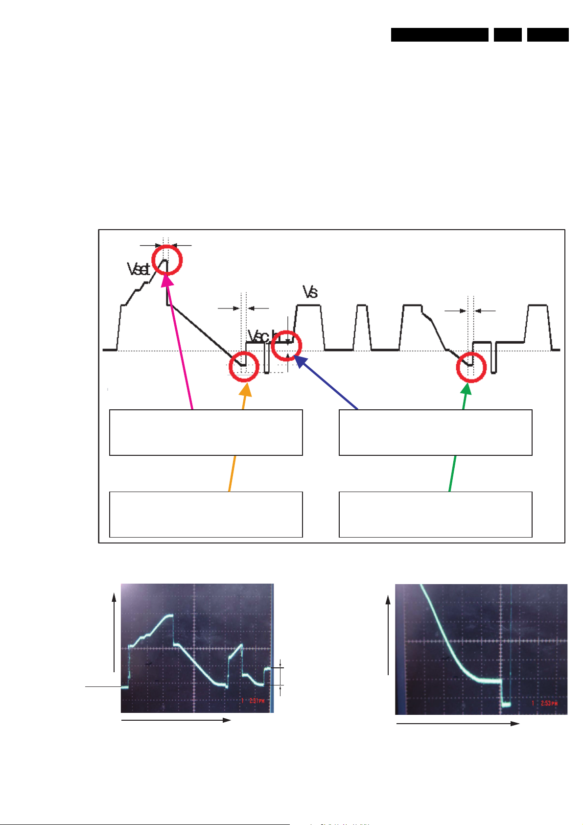
Alignments
Adjust VR5001 to set the time of Yfr
(Falling Ramp_1st) 35 µs
Adjust VR5002 to set the time of
Yfr (Falling Ramp_3rd) 20 µs
Adjust VR5000 to set the time of
Yrr( Rising Ramp) 50 µs
Adjust VR5901 to set the voltage of
Vsch [Scan high voltage ] 25V
(V)
20V/div.
50ms/div.
(t)
EN 65SDI PDP 8.
8.7 Alignments 50" HD v3
1. Put the dipswitches on the Logic Board in the internal
position to get a Full White Pattern (see Figure “DIP switch
positions”).
2. Adjust Vsch to 25 V by using VR5901_VSC_h (Vsc_h
should be connected to "+" unit of DMM).
3. Check the waveform using Oscilloscope.
• Triggering through V_TOGG of LOGIC Board.
• Connect the OUT 4 Test Point at the centre of Y_buffer
to other channel, and then check the first Subfield
operating waveform of one TV-Field.
• Check the waveform again after adjusting Horizontal
Division. Check the Reset waveform when the
V_TOGG Level is changed.
• Set the Rising Ramp Flat Time to 50 µs by adjusting
VR5000. GND maintenance section should be
checked after the Vertical Division is readjusted to “2 V
or 5 V”.
• Set the Falling maintenance time to 35 µs by adjusting
VR5001.
• Change the waveform position of Oscilloscope to the
3rd Subfield and then set the Falling maintenance time
to 20µs by adjusting the VR5002.
• GND maintenance section should be checked after the
Vertical Division is readjusted to “2 V or 5 V”.
Special notice: When you adjust the inclination of waveform,
do check and adjustment being based on the Reset waveform
of 1st Sub-field of 1st Frame and then move to 3rd Sub-field for
adjusting.
(V)
50V/div.
DC=0V
Figure 8-38 Rising ramp
Figure 8-37 TCP ramp waveform inclination adjustment (Y-Board)
40V
20ms/div.
(t)
Figure 8-39 Falling ramp
Page 66
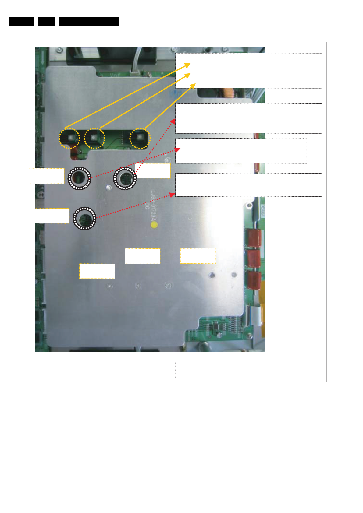
EN 66 SDI PDP8.
* Pay close attention to above adjustment
1. VR5901(Vscan_h) / Adjustment; 25V
2. VR5901/(Vscan) / Adjustment; -90V
3. VR5901/ Adiustment; Fix
4. VR5000 Adjustment: Rising Ramp flat time:
=> Typ. 50 µsec
6. VR5002 Adjustment : 3th SF Falling Ramp flat time
=> Typ. 20 µsec
5. VR5001 Adjustment : Falling Ramp flat time
=> Typ. 35 µsec
VR5004 VR5005
VR5001
VR5000
VR5002
VR5006
Alignments
Figure 8-40 Potentiometer locations
Page 67
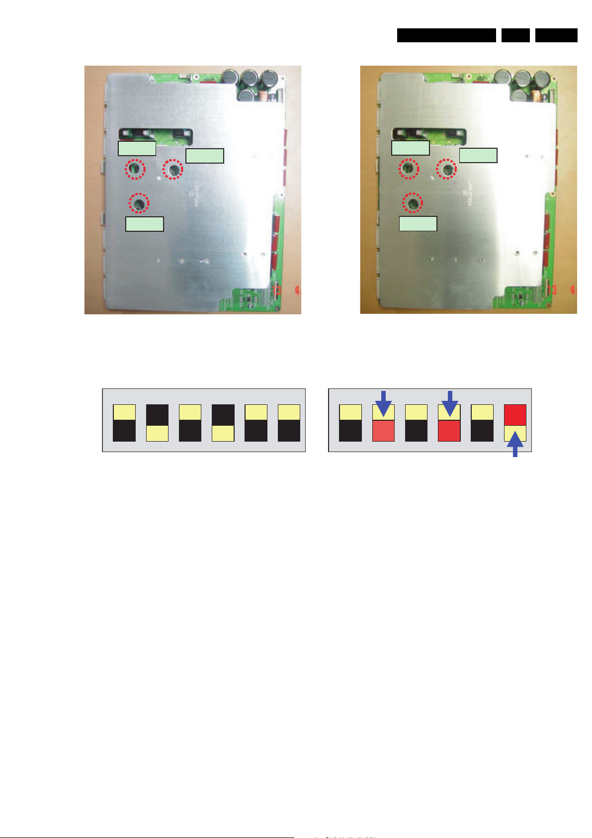
Alignments
GXWW
\y}
GWWW\y}
GYWW
\y}
sq`YTW
W_\Zh
F_14991_076.eps
140206
GXWW\y}
GWWW\y}
GYWW\y}
sq`YTWW_\Zi
F_14991_077.eps
140206
EN 67SDI PDP 8.
Figure 8-41 Potentiometer locations LJ92-00853A Figure 8-42 Potentiometer locations LJ92-00853B
<External>
<Internal>
F_14991_050.eps
230306
Figure 8-43 DIP switch positions
Page 68
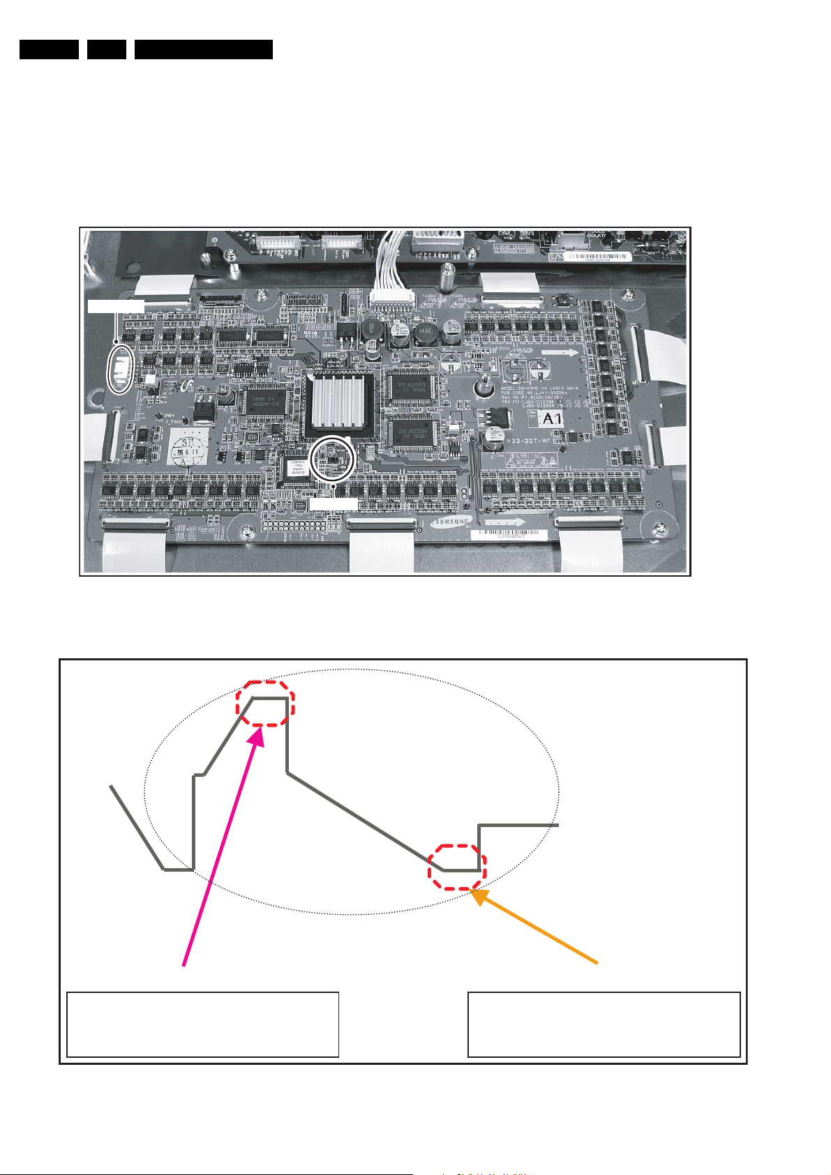
EN 68 SDI PDP8.
F_14991_052.eps
081105
ComPair
CN2012
Alignments
8.8 Alignments 50" HD v4
1. Get Pattern to be Full White (place jumper CN2012 on
Logic Board).
2. Locate all testpoints and potentiometers of the board at
hand.
• Triggering through V_TOGG of LOGIC Board.
• Connect the CN5511 Test Point at the Y_buffer to
other channel, and then check the first Subfield
operating waveform of one TV-Field.
• Check the waveform again after adjusting Horizontal
Division. Check the Reset waveform when the
V_TOGG Level is changed.
• Set the Rising Ramp Flat Time to 90 µs by adjusting
VR5000.
• Set the Falling maintenance time to 80 µs by adjusting
VR5001.
Figure 8-44 Jumper CN2012 / ComPair connector on v4 Logic board
1stSub Field
Adjust VR5000 to set the time of
Yrr (Main Reset Rising Ramp) 90 us
Adjust VR5001 to set the time of
Yfr (Main Reset Falling Ramp) 80 us
F_14991_020.eps
030805
Page 69
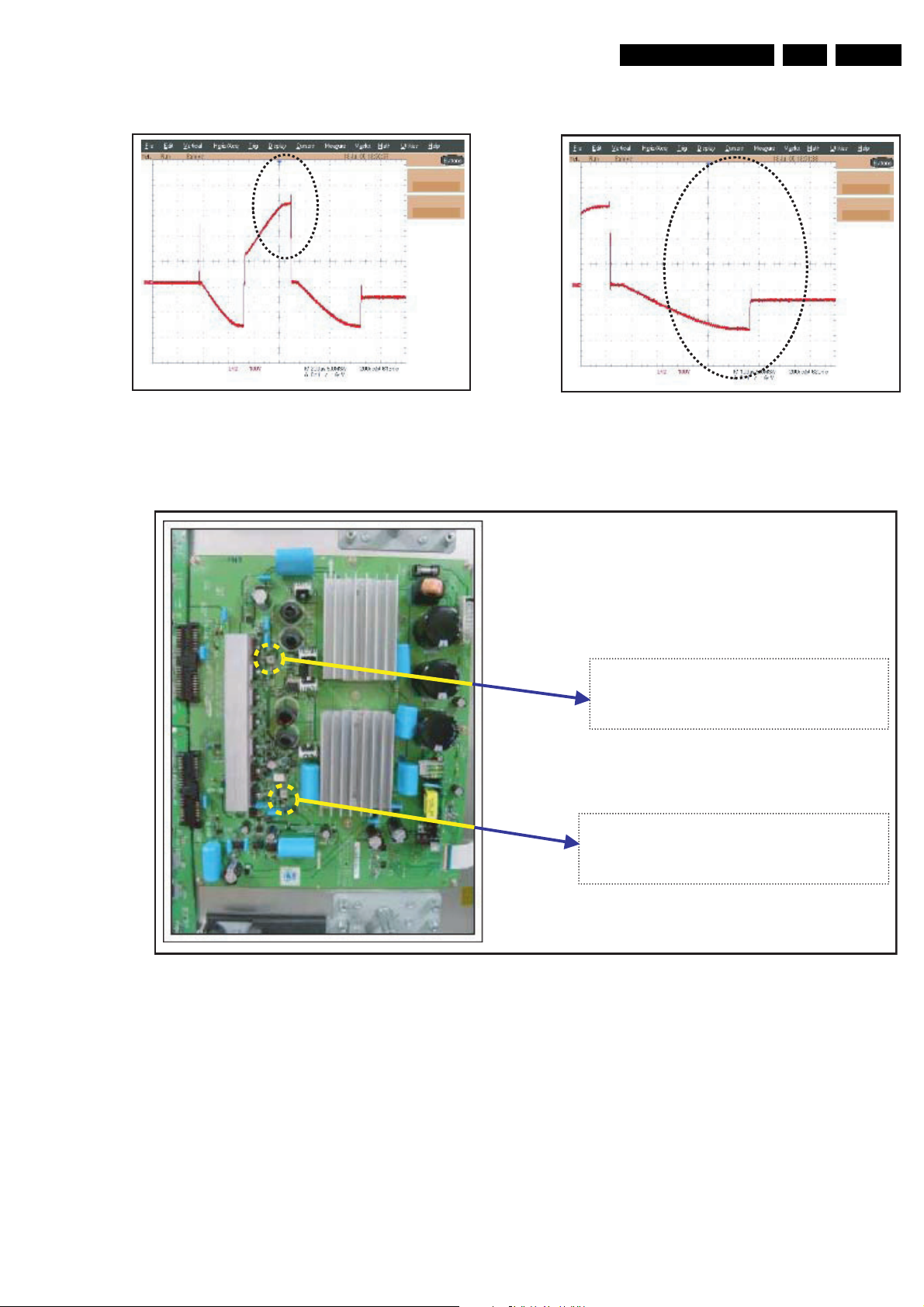
Alignments
F_14991_021a.eps
030805
F_14991_021b.eps
030805
F_14991_022.eps
030805
VR5001 Adjustment :
Falling Ramp
T
yp. 80usec
VR5000 Adjustment
:
Rising Ramp flat time => Typ. 90use
c
flat time =>
Figure 8-45 TCP ramp waveform inclination adjustment (Y-Board)
EN 69SDI PDP 8.
Figure 8-46 Rising ramp
Figure 8-47 Falling ramp
Figure 8-48 Potentiometer locations
Page 70
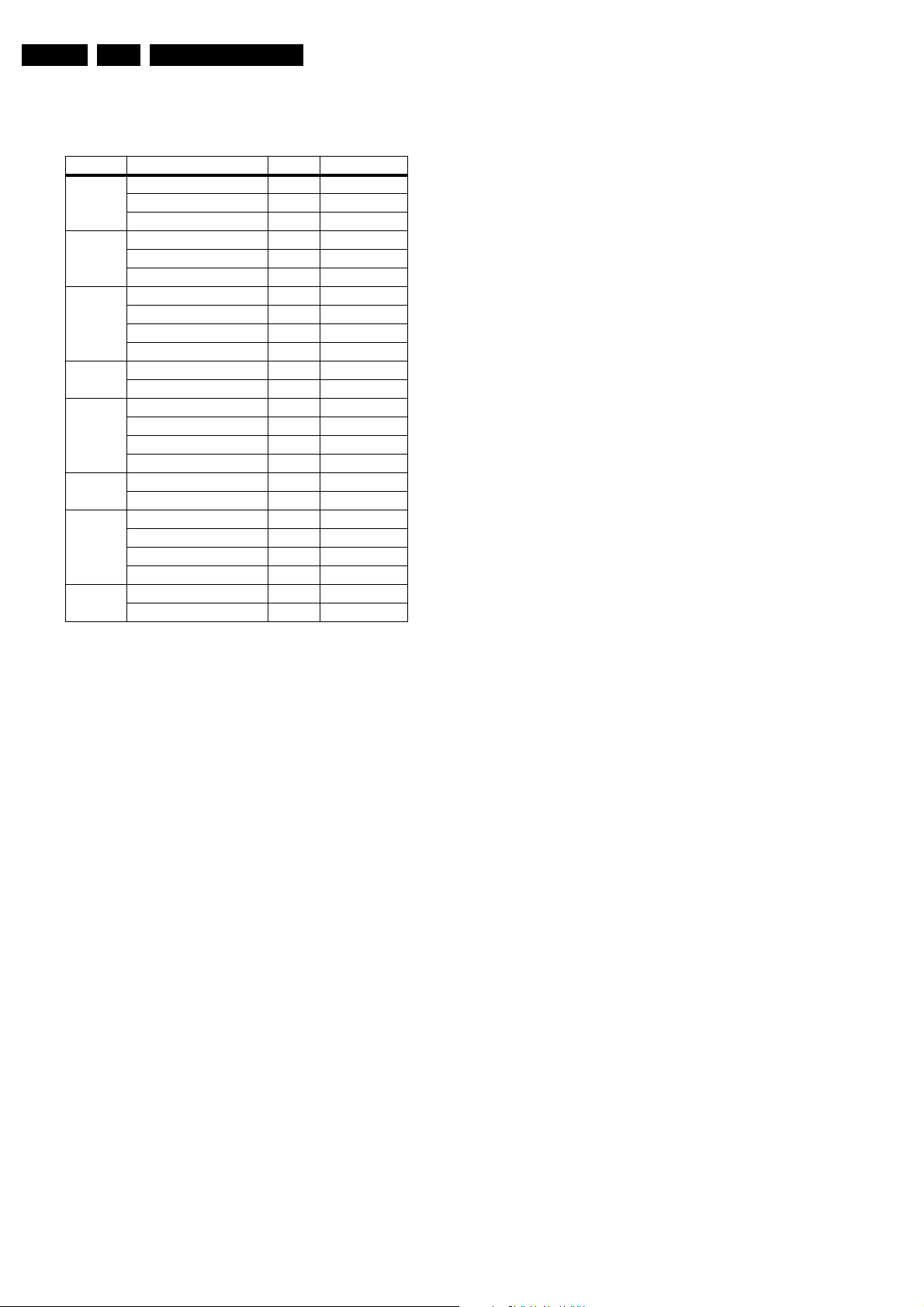
EN 70 SDI PDP8.
Alignments
8.9 Alignment value overview (all screens)
Table 8-1 Alignment table Y PWB
Model Wave Form Item Default
37"SD v4 Rising_Ramp VR5001 30 µs (30 ~ 40)
Falling_Ramp_1st VR5002 16 µs (10 ~ 20)
Vsch VR5000 38 V
42" SD v2 Rising_Ramp (Vset) VR5003 10 µs
-Vsc 1 VR5001 20 µs
-Vsc 2 VR5002 5 µs
42" SD v3 Rising_Ramp VR5002 10 µs
Falling_Ramp_1st VR5003 30 µs
Falling_Ramp_3rd VR5001 30 µs
Vsch VR5004 40 V
42" SD v4 Rising_Ramp VR5001 60 µs
Falling_Ramp_1st VR5003 80 µs
42" HD v3 Rising_Ramp VR5002 10 µs
Falling_Ramp_1st VR5003 20 µs
Falling_Ramp_3rd VR5001 10 µs
Vsch Scan high voltage VR5004 40 V
42" HD v4 Rising_Ramp VR5001 15 V
Falling_Ramp_1st VR5002 50 µs
50" HD v3 Rising_Ramp VR5000 50 µs
Falling_Ramp_1st VR5001 35 µs
Falling_Ramp_3rd VR5002 20 µs
Vsch Scan high voltage VR5901 25 V
50" HD v4 Rising_Ramp VR5001 90 µs
Falling_Ramp_1st VR5003 80 µs
Page 71

Circuit Descriptions, Abbreviation List, and IC Data Sheets
9. Circuit Descriptions, Abbreviation List, and IC Data Sheets
EN 71SDI PDP 9.
Index of this chapter:
9.1 Main function of Each Assembly
9.2 Abbreviation List
9.3 IC Data Sheets
9.1 Main function of Each Assembly
9.1.1 X Main Board
The X Main board generates a drive signal by switching the
FET in synchronization with logic main board timing, and
supplies the X electrode of the panel with the drive signal
through the connector.
1. Maintain voltage waveforms (including ERC).
2. Generate X rising ramp signal.
3. Maintain Ve bias between Scan intervals.
9.1.2 Y Main Board
The Y Main board generates a drive signal by switching the
FET in synchronization with the logic Main Board timing and
sequential supplies the Y electrode of the panel with the drive
signal through the scan driver IC on the Y-buffer board. This
board connected to the panel’s Y terminal has the following
main functions.
1. Maintain voltage waveforms (including ERC).
2. Generate Y-rising Falling Ramp.
3. Maintain V scan bias.
9.1.3 Logic Main Board
The Logic Main board generates and outputs the address drive
output signal and the X,Y drive signal by processing the video
signals. This Board buffers the address drive output signal and
feeds it to the address drive IC (COF module, video signal- X Y
drive signal generation, frame memory circuit / address data
rearrangement).
9.2 Abbreviation List
AC Alternating Current
COF Circuit On Foil
DC Direct Current
ERC Energy Recovery Circuit
ESD Electro Static Discharge
FET Field Effect Transistor
FFC Flat Foil Cable
FPC Flexible Printed Circuit
FTV Flat TeleVision
HD High Definition
I/O Input/Output
IC Integrated Circuit
LB Logic Buffer
LED Light Emitting Diode
LVDS Low Voltage Differential Signalling
PCB Printed Circuit Board (same as PWB)
PDP Plasma Display Panel
PSU Power Supply Unit
PWB Printed Wiring Board (same as PCB)
RGB Red, Green, Blue colour space
SD Standard Definition
SDI Samsung Display Industry (supplier)
SMPS Switched Mode Power Supply
SSB Small Signal Board
SF Sub Field
TCP Tape Carrier Package
VR Variable Resistor
Vsc Scan Voltage
YBL Y Buffer Lower board
YBU Y Buffer Upper board
YM Y Main board
9.3 IC Data Sheets
Not applicable.
9.1.4 Logic Buffer (E, F)
The Logic Buffer transmits data signal and control signal.
9.1.5 Y Buffer Board (Upper, Lower)
The Y Buffer board consisting of the upper and lower boards
supplies the Y-terminal with scan waveforms. The board
comprises eight scan driver ICs (ST microelectronics STV
7617: 64 or 65 output pins), but four ICs for the SD class.
9.1.6 AC Noise Filter
The AC Noise filter has function for removing noise (low
frequency) and blocking surge. It affects safety standards
(EMC, EMI).
9.1.7 TCP (Tape Carrier Package)
The TCP applies the Va pulse to the address electrode and
constitutes address discharge by the potential difference
between the Va pulse and the pulse applied to the Y electrode.
The TCP comprise four data driver ICs (STV7610A: 96 pins
output pins). Seven TCPs are required for signal scan.
Page 72
EN 72 SDI PDP10.
10. Spare Parts List
Notes;
• Determine the SDI part / model number of the PDP
• Find the SDI part number on the actual board to be
replaced.
SDI part number begin with “LJ92” and for the SMPS and
sub SMPS the part number will begin with “LJ44”.
• Find the SDI board part number in the spare parts
overview.
• Find the SDI part number in this overview that matches the
part number that is actually on the original board.
• Cross the SDI board part number to the philips part
number.
• Order the philips part number.
Table 10-1 Spare parts overview 37" SD v4
PDP type 37" SD v4
PDP 12NC 9322 217 39682 (8204 000 77261)
PDP model type and version S37SD-YD02
Remarks
Boards Codes for lead type PWB’s Codes for lead-free type PWB’s
Logic-Buffer (E) LJ92-00976A 9965 000 26187 LJ92-01138B 9965 000 32616 N
Logic-Buffer (F) LJ92-00977A 9965 000 26188 LJ92-01139B 9965 000 32617 N
Logic-Buffer (G) LJ92-01002A 9965 000 26189 LJ92-01140B 9965 000 32618 N
Logic-Buffer (H)- ----
Logic-Buffer (I)- ----
Logic-Buffer (J)- ----
Y-Buffer (up) LJ92-01022A 9965 000 26190 LJ92-01147A 9965 000 32619 N
Y-Buffer (down)- ----
Logic-Board LJ92-01056A (See Kit 1 Note)
SUBL - ----
SUBR - ----
X-Board LJ92-01020A 9965 000 26192 LJ92-01268A 9965 000 32620 N
Y-Board LJ92-01021A 9965 000 26193 LJ92-01149B 9965 000 32621 N
SMPS (PSU) LJ44-00084A 9965 000 26194 LJ44-00084B 9965 000 32622 Y
SUB PSU LJ44-00075A 9965 000 25131 LJ44-00075B 9965 000 32623 Y
Lead type boards being not compatible with lead free type
LJ92-01145A (See Kit 2 Note)
Spare Parts List
will not be phased out
9965 000 26191 LJ92-01257A 9965 000 29322 N
• Note: The appearance of a leaded and lead-fraa board can
be different; the colour of the PWB and also the layout of
the components are sometimes different.
E_06532_026.eps
081105
Figure 10-1 Lead-free logo SDI
Lead Free type
being compatible
with Lead type
PWB
Kit 1 LJ93-00205A 9965 000 33796
Kit 2 LJ93-00204A 9965 000 33797
Note:
Kit 1: 37" FCR kit concists of 4 boards ( Logic + Y-main + Y and
E buffer)
reference Symptom Cure information TV-05/0006
CORRECTION XI: PDP with "Lead" boards and use of Logic
board (LJ92-01056A):
Replace the Logic board, the Y-Main board, the Y-buffer board,
and the Logic buffer E board together.
These four boards are available in Service Kit number 1 (with
order code 9965 000 33796 (LJ93-00205A)).
The content of Service Kit number 1 is:
* Logic main board 9965 000 29322 (LJ92-01257A).
* Y-Main board 9965 000 32621 (LJ92-01149B).
* Y-Buffer board 9965 000 32619 (LJ92-01147A).
* Logic-Buffer E 9965 000 32616 (LJ92-01138B).
Note:
FCR Kit: = False contouring reduction kit
Note:
Kit 2: 37" FCR kit concists of 2 boards (logic + Y-main)
reference Symptom Cure information TV-05/0006
CORRECTION XI
PDP with "Lead-free" boards and use of Logic board (LJ9201145A):
Replace the Logic board and the Y-Main board together. These
two boards are available in Service Kit number 2 (with order
code 9965 000 33797 (LJ93-00204A)).
The content of Service Kit number 2 is:
* Logic main board 9965 000 29322 (LJ92-01257A).
* Y-Main board 9965 000 32621 (LJ92-01149B).
3) PDP with "Lead-free" boards and use of Logic board (LJ92-
01257A):
In case this PDP has a defective board, replace this defective
board only
Page 73
Spare Parts List
EN 73SDI PDP 10.
Table 10-2 Spare parts overview 42" SD v2
PDP type 42"SDv2
PDP model 12NC 9322 195 45682
PDP model type and version S42SD-YD06
Remarks
Boards PWB Codes
Logic-Buffer (E) LJ92-00632A 9965 000 17726
Logic-Buffer (F) LJ92-00633A 9965 000 17725
Logic-Buffer (G) LJ92-00634A 9965 000 17724
Logic-Buffer (H) - -
Logic-Buffer (I) - -
Logic-Buffer (J) - -
Y-Buffer (up) LJ92-00751A 9965 000 17727
Y-Buffer (down) LJ92-00750A 9965 000 17728
Logic-Board LJ92-00818A 9965 000 17729
SUBL - -
SUBR - -
X-Board LJ92-00998A 9965 000 17720
Y-Board LJ92-00999A 9965 000 17731
SMPS (PSU) LJ44-00049A 9965 000 17730
SUB PSU - -
Codes for lead type PWBs (this model has been produced
with leaded type PWB’s only)
Table 10-3 Spare parts overview 42" SD v3
PDP type 42" SD v3
PDP model 12NC 9322 215 27682
PDP model type and version S42SD-YD05
Remarks Lead type boards being phased out
Boards Codes for leaded type PWBs Codes for lead-free type PWBs
Logic-Buffer (E) LJ92-00811A 9965 000 25109 LJ92-00811B 9965 000 32624 Y
Logic-Buffer (F) LJ92-00812A 9965 000 25110 LJ92-00812B 9965 000 32625 Y
Logic-Buffer (G) LJ92-00813A 9965 000 25111 LJ92-00813B 9965 000 32626 Y
Logic-Buffer (H)-----
Logic-Buffer (I)-----
Logic-Buffer (J)-----
Y-Buffer (up) LJ92-00796A 9965 000 25112 LJ92-01285A 9965 000 32376 Y
Y-Buffer (down) LJ92-00797A 9965 000 25113 LJ92-01286A 9965 000 32377 Y
Logic-Board LJ92-00975D 9965 000 25114 LJ92-01247D 9965 000 32378 N (tbd)
SUBL -----
SUBR -----
X-Board LJ92-00943A 9965 000 25115 LJ92-01283A 9965 000 32627 Y
Y-Board LJ92-00944B 9965 000 25116 LJ92-01284A 9965 000 32379 Y
SMPS (PSU) LJ44- 000 58A 9965 000 25108 LJ44-00058B 9965 000 32638 Y
SUB PSU LJ44- 000 75A 9965 000 25131 LJ44-00075B 9965 000 32623 Y
Lead Free type
being compatible
with Lead type
PWB
Table 10-4 Spare parts overview 42" SD v4 (Part 1)
PDP type 42" SD v4
PDP model 12NC 9322 226 37682
PDP model type and version S42SD-YD07 (*) S42SD-YD07 (PP42SD015A)
Remarks
Logic-Buffer (E) LJ92-01026A 9965 000 29205 LJ92-01026A 9965 000 29205 Y
Logic-Buffer (F) LJ92-01027A 9965 000 29206 LJ92-01027A 9965 000 29206 Y
Logic-Buffer (G) - - - - -
Logic-Buffer (H) - - - - -
Logic-Buffer (I) - - - - -
Logic-Buffer (J) - - - - -
Y-Buffer (up) LJ92-01031A 9965 000 29207 LJ92-01031A 9965 000 29207 Y
Y-Buffer (down) LJ92-01032A 9965 000 29208 LJ92-01032A 9965 000 29208 Y
Logic-Board LJ92-01274D 9966 000 30042 LJ92-01274D 9966 000 30042 Y
SUBL -----
SUBR -----
X-Board LJ92-01029A 9965 000 29204 LJ92-01336A 9965 000 32628 Y
Y-Board LJ92-01030A 9965 000 29209 LJ92-01337A 9965 000 32629 Y
SMPS (PSU) LJ44-00092B 9965 000 29210 LJ44-00101A 9965 000 29210 N (tdb)
SUB PSU - - - - -
No supply of new SMPS LJ44-00092B.
Compatibility with LJ44-00101C + cable: tdb (15/2)
Version number used by SDI:PP42SD015B(SMPS Rev.0.55)
New SMPS supply:LJ44-00101C + cables. Service
information: tbd
Boards from
PP42SD015A
and
S42SD-YD07 (*)
being
compatible
Page 74
EN 74 SDI PDP10.
Table 10-5 Spare parts overview 42" SD v4 (Part 2)
Spare Parts List
PDP type 42" SD v4 Service Information
PDP model 12NC 9322 226 96682 9322 233 81682
PDP model type and version S42SD-YD07 (PP42SD015B) S42SD-YD07 (PP42SD015F)
Version number used by
Remarks
Logic-Buffer (E) LJ92-01026A 9965 000 29205 Y LJ92-01026A 9965 000 29205 Y
Logic-Buffer (F) LJ92-01027A 9965 000 29206 Y LJ92-01027A 9965 000 29206 Y
Logic-Buffer (G) - - - - - -
Logic-Buffer (H) - - - - - -
Logic-Buffer (I) - - - - - -
Logic-Buffer (J) - - - - - -
Y-Buffer (up) LJ92-01031A 9965 000 29207 Y LJ92-01031A 9965 000 29207 Y
Y-Buffer (down) LJ92-01032A 9965 000 29208 Y LJ92-01032A 9965 000 29208 Y
Logic-Board LJ92-01274D 9966 000 30042 Y LJ92-01274D 9966 000 30042 Y
SUBL - - - - - -
SUBR - - - - - -
X-Board LJ92-01336A 9965 000 32628 Y LJ92-01336A 9965 000 32628 Y
Y-Board LJ92-01337A 9965 000 32629 Y LJ92-01337A 9965 000 32629 Y
SMPS (PSU) LJ44-00101B 9965 000 32630 N LJ44-00101C 9965 000 33880 Y
SUB PSU - - - - - -
SDI:PP42SD015B(SMPS Rev.0.55)
New SMPS supply:LJ44-00101C +
cables. Service information: tbd
PWB’s from
PP42SD015B and
PP42SD015A
being compatible
Version number used by SDI: PP42SD015F (SMPS
Rev.0.7)
932223381682
being backwards
compatible tbd
PWB’s from
PP42SD015B and
PP42SD015F
being compatible
Table 10-6 Spare parts overview 42" HD v3
PDP type 42" HD v3
PDP model 12NC 9322 215 25682
PDP model type and version S42AX-XD02
Remarks Lead type boards being phased out
Boards Codes for leaded type PWBs Codes for lead-free type PWBs
Logic-Buffer (E) LJ92-00895A 9965 000 25101 LJ92-01264A 9965 000 32631 Y
Logic-Buffer (F) LJ92-00896A 9965 000 25102 LJ92-01265A 9965 000 32632 Y
Logic-Buffer (G)-----
Logic-Buffer (H)-----
Logic-Buffer (I)-----
Logic-Buffer (J)-----
Y-Buffer (up) LJ92-00993A 9965 000 25103 LJ92-00993B 9965 000 32633 Y
Y-Buffer (down) LJ92-00994A 9965 000 25104 LJ92-00994B 9965 000 32634 Y
Logic-Board LJ92-00990E 9965 000 25105 LJ92-01221C 9965 000 32635 Y
SUBL -----
SUBR-----
X-Board LJ92-00980A 9965 000 25106 LJ92-00980B 9965 000 32636 Y
Y-Board LJ92-00981A 9965 000 25107 LJ92-00981B 9965 000 32637 Y
SMPS (PSU) LJ44-00058A 9965 000 25108 LJ44-00058B 9965 000 32638 Y
SUB PSU LJ44-00075A 9965 000 25131 LJ44-00075B 9965 000 32623 Y
Lead Free type
being compatible
with Lead type
PWB
Table 10-7 Spare parts overview 42" HD v4 (Part 1)
PDP type 42" HD v4
PDP model 12NC 8204 000 78191 9322 225 38682
PDP model type and version S42AX-YD01 (*) S42AX-YD01 (PP42AX-007A)
Remarks
Logic-Buffer (E) LJ92-01054A 9965 000 29197 LJ92-01054A 9965 000 29197 Y
Logic-Buffer (F) LJ92-01055A 9965 000 29198 LJ92-01055A 9965 000 29198 Y
Logic-Buffer (G)-----
Logic-Buffer (H)-----
Logic-Buffer (I)-----
Logic-Buffer (J)-----
Y-Buffer (up) LJ92-01117A 9965 000 29199 LJ92-01202A 9965 000 32639 Y
Y-Buffer (down) LJ92-01118A 9965 000 29200 LJ92-01203A 9965 000 32640 Y
Logic-Board LJ92-01053A 9965 000 29203 LJ92-01270B 9965 000 32641 Y
SUBL-----
SUBR-----
X-Board LJ92-01115A 9965 000 29196 LJ92-01199A 9965 000 32642 Y
Y-Board LJ92-01200A 9965 000 32643 LJ92-01200A 9965 000 32643 Y
SMPS (PSU) LJ44-00092A 9965 000 29202 LJ44-00101A 9965 000 29210 N
SUB PSU-----
SMPS LJ44-00092A being phased out
supply:LJ44-00101C + cables. Service information: tbd
(SMPS Rev.0.55) New SMPS supply:LJ44-00101C + cables.
Service information: tbd
Boards from
S42AX-YD01(*)
and PP42AX007A being
Compatible
Page 75
Table 10-8 Spare parts overview 42" HD v4 (Part 2)
Spare Parts List
EN 75SDI PDP 10.
PDP type 42" HD v4 Service
PDP model 12NC 9322 226 95682 9322 233 80682
PDP model type and version S42AX-YD01 (PP42AX-008A) PWB’s from
Remarks
Logic-Buffer (E) LJ92-01054A 9965 000 29197 Y LJ92-01054A 9965 000 29197 Y
Logic-Buffer (F) LJ92-01055A 9965 000 29198 Y LJ92-01055A 9965 000 29198 Y
Logic-Buffer (G) - - - - - -
Logic-Buffer (H) - - - - - -
Logic-Buffer (I) - - - - - -
Logic-Buffer (J) - - - - - -
Y-Buffer (up) LJ92-01202A 9965 000 32639 Y LJ92-01202A 9965 000 32639 Y
Y-Buffer (down) LJ92-01203A 9965 000 32640 Y LJ92-01203A 9965 000 32640 Y
Logic-Board LJ92-01270B 9965 000 32641 Y LJ92-01270B 9965 000 32641 Y
SUBL - - - - - -
SUBR - - - - - -
X-Board LJ92-01199A 9965 000 32642 Y LJ92-01199A 9965 000 32642 Y
Y-Board LJ92-01200A 9965 000 32643 Y LJ92-01200A 9965 000 32643 Y
SMPS (PSU) LJ44-00101B 9965 000 32630 N LJ44-00101C 9965 000 33880 Y
SUB PSU - - - - - -
(SMPS Rev.0.65) New SMPS supply:LJ4400101C + cables. Service information: tbd
PP42AX-007A
and
PP42AX-008A
being
Compatible
(SMPS Rev.0.55) New SMPS supply:LJ44-00101C + cables.
S42AX-YD01 (PP42AX-008B)
Service information: tbd
Information 9322
233 80682 being
backwards
compatible tbd
PWB’s from
PP42AX-008A
and
PP42AX-008B
being compatible
Table 10-9 Spare parts overview 50" HD v3
PDP type 50" HD v3
PDP model 12NC 9322 215 26682
PDP model type and version S50HW-XD03 (PP50HW004C)
Remarks Lead type boards being phased out Lead Free type
Boards Codes for leaded type PWBs Codes for lead-free typePWBs
Logic-Buffer (E) LJ92-00917A 9965 000 25117 LJ92-00917B 9965 000 32614 Y
Logic-Buffer (F) LJ92-00918A 9965 000 25118 LJ92-00918B 9965 000 32615 Y
Logic-Buffer (G) LJ92-00919A 9965 000 25119 LJ92-00919B 9965 000 32646 Y
Logic-Buffer (H) LJ92-00920A 9965 000 25120 LJ92-00920B 9965 000 32647 Y
Logic-Buffer (I) LJ92-00921A 9965 000 25121 LJ92-00921B 9965 000 32648 Y
Logic-Buffer (J) LJ92-00922A 9965 000 25122 LJ92-00922B 9965 000 32649 Y
Y-Buffer (up) LJ92-00880A 9965 000 25123 LJ92-00880B 9965 000 32650 Y
Y-Buffer (down) LJ92-00881A 9965 000 25124 LJ92-00881B 9965 000 32651 Y
Logic-Board LJ92-00949C 9965 000 25125 LJ92-01224B 9965 000 32652 Y
SUBL LJ92-00923A 9965 000 25126 LJ92-00923B 9965 000 32653 Y
SUBR LJ92-00959A 9965 000 25127 LJ92-00959B 9965 000 32654 Y
X-Board LJ92-00852A 9965 000 25128 LJ92-00852B 9965 000 32655 Y
Y-Board LJ92-00853A 9965 000 25129 LJ92-00853B 9965 000 32656 Y
SMPS (PSU) LJ44-000 65A 9965 000 25130 LJ44-00065B 9965 000 32657 Y
SUB PSU LJ44-000 99A 9965 000 26195 LJ44-00099B 9965 000 32658 Y
being compatible
with Lead type
PWB
Page 76
EN 76 SDI PDP10.
Spare Parts List
Table 10-10 Spare parts overview 50" HD v4 (Part 1)
PDP type 50" HD v4
PDP model 12NC 9322 226 54682 9322 226 97682
PDP model type and version S50HW-XD04 (PP50HW-005A) S50HW-XD04 (PP50HW-005B)
Remarks
Logic-Buffer (E) LJ92-01103A 9965 000 30025 LJ92-01103A 9965 000 30025 Y
Logic-Buffer (F) LJ92-01104A 9965 000 30026 LJ92-01104A 9965 000 30026 Y
Logic-Buffer (G) LJ92-01105A 9965 000 30027 LJ92-0110 5A 9965 000 30027 Y
Logic-Buffer (H) - - - - -
Logic-Buffer (I) - - - - -
Logic-Buffer (J) - - - - -
Y-Buffer (up) LJ92-01047A 9965 000 30028 LJ92-01047A 9965 000 30028 Y
Y-Buffer (down) LJ92-01048A 9965 000 30029 LJ92-01048A 9965 000 30029 Y
Logic-Board LJ92-01269B 9965 000 30032 LJ92-01269B 9965 000 30032 Y
SUBL - - - - -
SUBR - - - - -
X-Board LJ92-01045A 9965 000 30024 LJ92-01045A 9965 000 30024 Y
Y-Board LJ92-01046A 9965 000 30030 LJ92-01046A 9965 000 30030 Y
SMPS (PSU) LJ44-00108A 9965 000 33390 LJ44-00108B 9965 000 30031 N
SUB PSU - - - - -
Codes for PWBs from 932222654682 PP50H-005A
New SMPS supply:LJ44-00108C + cables.
Service information: tbd
Codes for PWBs from 932222697682 PP50H-005B
New SMPS supply:LJ44-00108C + cables.
Service information: tbd
Table 10-11 Spare parts overview 50" HD v4 (Part 2)
PWB’s from
PP50HW-005A and
PP50HW-005B
being compatible
PDP type 50" HD v4 Service
PDP model 12NC 9322 233 79682
PDP model type and version S50HW-XD04 (PP50HW-005B) PWB’s from
Remarks Codes for PWBs from 932223379682 PP50H-005E
Logic-Buffer (E) LJ92-01103A 9965 000 30025 Y
Logic-Buffer (F) LJ92-01104A 9965 000 30026 Y
Logic-Buffer (G) LJ92-01105A 9965 000 30027 -
Logic-Buffer (H) - - -
Logic-Buffer (I) - - -
Logic-Buffer (J) - - -
Y-Buffer (up) LJ92-01047A 9965 000 30028 Y
Y-Buffer (down) LJ92-01048A 9965 000 30029 Y
Logic-Board LJ92-01269B 9965 000 30032 Y
SUBL - - -
SUBR - - -
X-Board LJ92-01045A 9965 000 30024 Y
Y-Board LJ92-01046A 9965 000 30030 Y
SMPS (PSU) LJ44-00108C 9965 000 33879 Y
SUB PSU - - -
information:
932223379682
being backwards
compatible: tdb
PP50HW-005B and
PP50HW-005E
being compatible
Note: All 42- and 50-inch v4 panels are lead-free. Differences
in table above are related to the SMPS (PSU).
Page 77

11. Revision List
Manual xxxx xxx xxxx.0
• First release.
Manual xxxx xxx xxxx.1
• General: Update of whole manual to the latest publication
standards and information.
• 37" SD v4: Errors corrected, and info updated.
• 42" SD v2: Errors corrected, and info updated.
• 42" SD v3: Errors corrected, and info updated.
• 42” SD v4: New.
• 42" HD v3: Errors corrected, and info updated.
• 42" HD v4: New.
• 50" HD v3: Errors corrected, and info updated.
• 50" HD v4: New.
Manual xxxx xxx xxxx.2
• SMPS layouts and voltages updated
• Alignments updated
• Parts list updated
Manual xxxx xxx xxxx.3
• General: Correction of some minor errors.
• Chapter 8, Alignments: Errors corrected, and info
updated.
Revision List
EN 77SDI PDP 11.
Manual xxxx xxx xxxx.4
• Chapter 5, Service Modes, Error Codes, and Fault
Finding: References to LEDs corrected in Figure 5-7.
 Loading...