

Philips SCN2661AC1N28, SCN2661BA1F28, SCN2661BC1A28, SCN2661BC1F28, SCN2661BC1N28 Datasheet
...
INTEGRATED CIRCUITS
SCN2661/SCN68661
Enhanced programmable
communications interface (EPCI)
Product specification
IC19 Data Handbook
1994 Apr 27

Philips Semiconductors Product specification
Enhanced programmable communications
interface (EPCI)
DESCRIPTION
The Philips Semiconductors SCN2661 EPCI is a universal
synchronous/asynchronous data communications controller chip
that is an enhanced version of the SCN2651. It interfaces easily to
all 8-bit and 16-bit microprocessors and may be used in a polled or
interrupt driven system environment. The SCN2661 accepts
programmed instructions from the microprocessor while supporting
many serial data communications disciplines —synchronous and
asynchronous — in the full- or half-duplex mode. Special support
for BISYNC is provided.
The EPCI serializes parallel data characters received from the
microprocessor for transmission. Simultaneously, it can receive
serial data and convert it into parallel data characters for input to the
microcomputer.
The SCN2661 contains a baud rate generator which can be
programmed to either accept an external clock or to generate
internal transmit or receive clocks. Sixteen different baud rates can
be selected under program control when operating in the internal
clock mode. Each version of the EPCI (A, B, C) has a different set
of baud rates.
SCN2661/SCN68661
PIN CONFIGURATIONS
D2
1
D3
2
RxD
3
GND
4
D4
5
D5
6
D6
7
D7
8
/XSYNC
TxC
R/W
CE
9
A1
10
11
A0
12
13
14
DIP
28
27
26
25
24
23
22
21
20
19
18
17
16
15
D1
D0
V
CC
RxC/BKDET
DTR
RTS
DSR
RESET
BRCLK
TxD
/DSCHG
TxEMT
CTS
DCD
TxRDYRxRDY
FEA TURES
•Synchronous operation
– 5- to 8-bit characters plus parity
– Single or double SYN operation
– Internal or external character synchronization
– Transparent or non-transparent mode
– Transparent mode DLE stuffing (Tx) and detection (Rx)
– Automatic SYN or DLE-SYN insertion SYN, DLE and DLESYN
stripping
– Odd, even, or no parity
– Local or remote maintenance loopback mode
– Baud rate: DC to 1Mbps (1X clock)
•Asynchronous operation
– 5- to 8-bit characters plus parity
– 1, 1-1/2 or 2 stop bits transmitted
– Odd, even, or no parity
– Parity, overrun and framing error detection
– Line break detection and generation
– False start bit detection
– Automatic serial echo mode (echoplex)
– Local or remote maintenance loopback mode
– Baud rate: DC to 1Mbps
(1X clock)
DC to 62.5kbps (16X clock)
DC to 15.625kbps
(64X clock)
OTHER FEATURES
•Internal or external baud rate clock
•3 baud rate sets
•16 internal rates for each set
•Double-buffered transmitter and receiver
INDEX
CORNER
NOTE:
Pin Functions the same as 28-pin DIP.
41
5
11
TOP VIEW
26
25
PLCC
19
1812
SD00077
Figure 1. Pin Configurations
•Dynamic character length switching
•Full- or half-duplex operation
•TTL compatible inputs and outputs
•RxC and TxC pins are short-circuit protected
•Single +5V power supply
•No system clock required
APPLICATIONS
•Intelligent terminals
•Network processors
•Front-end processors
•Remote data concentrators
•Computer-to-computer links
•Serial peripherals
•BISYNC adaptors
1994 Apr 27 853-1070 12793
2
Philips Semiconductors Product specification
Enhanced programmable communications
interface (EPCI)
ORDERING CODE
VCC = +5V +5%
PACKAGES
28-Pin Ceramic Dual In-Line Package (cerdip) 0.6” Wide
28-Pin Plastic Dual In-Line Package (DIP) 0.6” Wide
28-Pin Plastic Lead Chip Carrier (PLCC)
BLOCK DIAGRAM
NOTES:
DATA BUS
D0–D7
RESET
R/W
BRCLK
TxC/SYNC
RxC
/BKDET
DSR
DCD
CTS
RTS
DTR
TxEMT/*
DSCHG
CE
A
0
A
1
DATA BUS
BUFFER
OPERATION CONTROL
MODE REGISTER 1
MODE REGISTER 2
COMMAND REGISTER
STATUS REGISTER
BAUD RATE
GENERATOR
AND
CLOCK CONTROL
MODEM
CONTROL
* Open–drain output pin.
Figure 2. Block Diagram
ABSOLUTE MAXIMUM RATINGS
SYMBOL
T
A
T
STG
NOTES:
1. Stresses above those listed under Absolute Maximum Ratings may cause permanent damage to the device. This is a stress rating only and
functional operation of the device at these or at any other condition above those indicated in the operation section of this specification is not
implied.
2. For operating at elevated temperatures, the device must be derated based on +150°C maximum function temperature.
3. This product includes circuitry specifically designed for the protection of its internal devices from the damaging effect of excessive static
charge. Nonetheless, it is suggested that conventional precautions be taken to avoid applying any voltages larger than the rated maxima.
4. Over recommended free-air operating temperature range and supply voltage range unless otherwise specified. For conditions shown as MIN
or MAX, use the appropriate value specified under recommended operating conditions.
Operating ambient temperature
Storage temperature -65 to +150 °C
All voltages with respect to ground
1
PARAMETER RATING UNIT
2
3
Commercial
0°C to +70°C
SCN2661BC1F28
SCN2661CC1F28
SCN2661AC1N28
SCN2661BC1N28
SCN2661CC1N28
SCN2661AC1A28
SCN2661BC1A28
SCN2661CC1A28
SNE/DLE CONTROL
SYN 1 REGISTER
SYN 2 REGISTER
DLE REGISTER
TRANSMITTER
TRANSMIT DATA
HOLDING REGISTER
SHIFT REGISTER
RECEIVE DATA
HOLDING REGISTER
SHIFT REGISTER
SCN2661/SCN68661
Industrial
-40°C to +85°C
SCN2661BA1F28
SCN2661CA1F28
Contact Factory SOT117-2
Contact Factory SOT261-3
TxRDY*
TRANSMIT
RECEIVER
RECEIVE
Note 4 °C
-0.5 to +6.0
TxD
RxRDY
RxD
SD00078
DWG #
0589B
*
V
1994 Apr 27
3
Philips Semiconductors Product specification
SYMBOL
PARAMETER
TEST CONDITIONS
UNIT
SYMBOL
PARAMETER
TEST CONDITIONS
UNIT
Enhanced programmable communications
interface (EPCI)
DC ELECTRICAL CHARACTERISTICS
Input voltage
V
IL
V
IH
Output voltage
V
OL
4
V
OH
I
IL
3-State output leakage current
I
LH
I
LL
I
CC
NOTES:
1. Over recommended free-air operating temperature range and supply voltage range unless otherwise specified. For conditions shown as MIN
or MAX, use the appropriate value specified under recommended operating conditions.
2. All voltages measurements are referenced to ground. All time measurements are at the 50% level for inputs (except t
0.8V and 2.0V for outputs. Input levels swing between 0.4V and 2.4V , with a transition time of ≤ 20ns maximum.
3. Typical values are at +25°C, typical supply voltages and typical processing parameters.
4. INTR
Low 0.8 V
High 2.0 V
Low IOL = 2.2mA 0.4 V
High IOH = -400µA 2.4 V
Input leakage current VIN = 0 to 5.5V 10 µA
Data bus high VO = 4.0V 10 µA
Data bus low VO = 0.45V 10 µA
Power supply current 150 mA
, TxRDY, RxRDY and TxEMT/DSCHG outputs are open-drain.
1, 2, 3
SCN2661/SCN68661
LIMITS
Min Typ Max
BRH
and t
BRL
) and at
CAP ACITANCE TA = 25°C, V
Capacitance
C
C
C
IN
OUT
I/O
Input 20 pF
Output
Input/Output Unmeasured pins tied to ground 20 pF
CC
= 0V
f
= 1MHz
C
LIMITS
Min Typ Max
20 pF
1994 Apr 27
4

Philips Semiconductors Product specification
SYMBOL
PARAMETER
TEST CONDITIONS
UNIT
Enhanced programmable communications
interface (EPCI)
AC ELECTRICAL CHARACTERISTICS
Pulse width
t
RES
t
CE
Setup and hold time
t
AS
t
AH
t
CS
t
CH
t
DS
t
DH
t
RXS
t
RXH
t
DD
7
t
DF
t
CED
Input clock frequency
f
BRG
f
BRG
6
f
R/T
Clock width
5
t
BRH
5
t
BRH
5
t
BRL
5
t
BRL
t
R/TH
6
t
R/TL
t
TXD
t
TCS
NOTES:
1. Over recommended free-air operating temperature range and supply voltage range unless otherwise specified. For conditions shown as MIN
or MAX, use the appropriate value specified under recommended operating conditions.
2. All voltages measurements are referenced to ground. All time measurements are at the 50% level for inputs (except t
0.8V and 2.0V for outputs. Input levels swing between 0.4V and 2.4V , with a transition time of ≤ 20ns maximum.
3. Typical values are at +25°C, typical supply voltages and typical processing parameters.
4. Parameter applies when internal transmitter clock is used.
5. Under test conditions of 5.0688MHz f
6. In asynchronous local loopback mode, using 1X clock, the following parameters apply: f
7. See AC load conditions.
Reset 1000 ns
Chip enable 250 ns
Address setup 10 ns
Address hold 10 ns
R/W control setup 10 ns
R/W control hold 10 ns
Data setup for write 150 ns
Data hold for write 10 ns
RX data setup 300 ns
RX data hold 350 ns
Data delay time for read
Data bus floating time for read
CE to CE delay 600 ns
Baud rate generator (2661A, B) 1.0 4.9152 4.9202 MHz
Baud rate generator (2661C) 1.0 5.0688 5.0738 MHz
TxC or RxC dc 1.0 MHz
Baud rate High (2661A, B) 75 ns
Baud rate High (2661C) 70 ns
Baud rate Low (2661A, B) 75 ns
Baud rate Low (2661C) 70 ns
TxC or RxC High 480 ns
TxC or RxC Low 480 ns
TxD delay from falling edge of TxC
Skew between TxD changing and falling edge
of TxC
output
4
BRG
1, 2, 3
(68661) and 4.9152MHz f
C
= 150pF
L
C
= 150pF
L
C
= 150pF
L
C
= 150pF
L
(68661A, B), t
BRG
and t
BRH
= 0.83MHz max and t
R/T
SCN2661/SCN68661
LIMITS
Min Typ Max
200 ns
100 ns
650 ns
0 ns
and t
BRH
measured at VIH and VIL, respectively.
BRL
= 700ns min.
R/TL
BRL
) and at
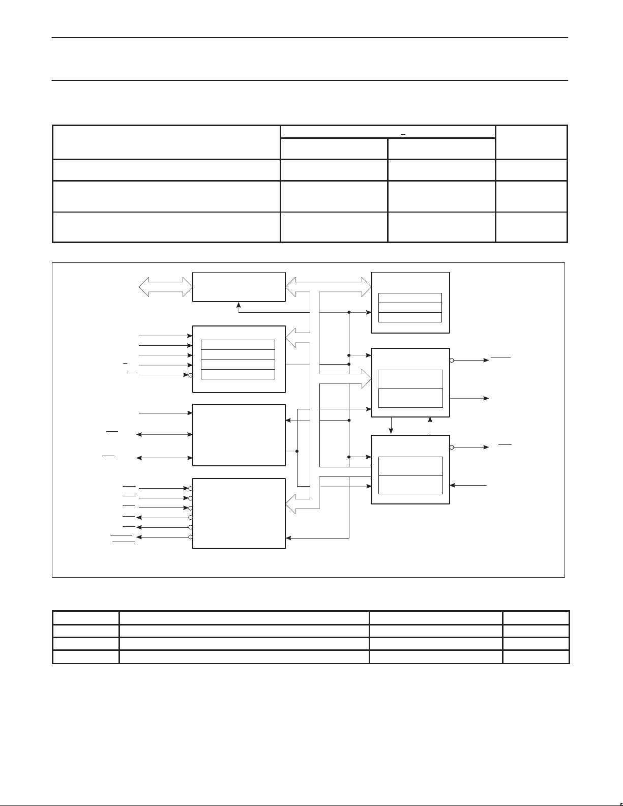
BLOCK DIAGRAM
The EPCI consists of six major sections. These are the transmitter,
receiver, timing, operation control, modern control and SYN/DLE
control. These sections communicate with each other via an
internal data bus and an internal control bus. The internal data bus
interfaces to the microprocessor data bus via a data bus buffer.
Operation Control
This functional block stores configuration and operation commands
from the CPU and generates appropriate signals to various internal
sections to control the overall device operation. It contains read and
write circuits to permit communications with the microprocessor via
the data bus and contains mode registers 1 and 2, the command
register, and the status register. Details of register addressing and
protocol are presented in the EPCI programming section of this data
sheet.
1994 Apr 27
Timing
The EPCI contains a Baud Rate Generator (BRG) which is
programmable to accept external transmit or receive clocks or to
divide an external clock to perform data communications. The unit
can generate 16 commonly used baud rates, any one of which can
be selected for full-duplex operation. See Table 1.
Receiver
The receiver accepts serial data on the RxD pin, converts this serial
input to parallel format, checks for bits or characters that are unique
to the communication technique and sends an “assembled”
character to the CPU.
Transmitter
The transmitter accepts parallel data from the CPU, converts it to a
serial bit stream, inserts the appropriate characters or bits (based on
5

Philips Semiconductors Product specification
Enhanced programmable communications
interface (EPCI)
the communication technique) and outputs a composite serial
stream of data on the TxD output pin.
Modem Control
The modern control section provides interfacing for three input
signals and three output signals used for “handshaking” and status
indication between the CPU and a modem.
Table 1. Baud Rate Generator Characteristics
68661A (BRCLK = 4.9152MHz)
MR23–20
0000 50 0.8kHz — 6144
0001 75 1.2 — 4096
0010 110 1.7598 –0.01 2793
0011 134.5 2.152 — 2284
0100 150 2.4 — 2048
0101 200 3.2 — 1536
0110 300 4.8 — 1024
0111 600 9.6 — 512
1000 1050 16.8329 0.196 292
1001 1200 19.2 — 256
1010 1800 28.7438 –0.19 171
1011 2000 31.9168 –0.26 154
1100 2400 38.4 — 128
1101 4800 76.8 — 64
1110 9600 153.6 — 32
1111 19200 307.2 — 16
BAUD RATE
ACTUAL FREQUENCY
16X CLOCK
SCN2661/SCN68661
SYN/DLE Control
This section contains control circuitry and three 8-bit registers
storing the SYN1, SYN2, and DLE characters provided by the CPU.
These registers are used in the synchronous mode of operation to
provide the characters required for synchronization, idle fill and data
transparency.
PERCENT
ERROR
DIVISOR
68661B (BRCLK = 4.9152MHz)
MR23–20
0000 45.5 0.7279kHz 0.005 6752
0001 50 0.8 — 6144
0010 75 1.2 — 4096
0011 110 1.7598 –0.01 2793
0100 134.5 2.152 — 2284
0101 150 2.4 — 2048
0110 300 4.8 — 1024
0111 600 9.6 — 512
1000 1200 19.2 — 256
1001 1800 28.7438 –0.19 171
1010 2000 31.9168 –0.26 154
1011 2400 38.4 — 128
1100 4800 76.8 — 64
1101 9600 153.6 — 32
1110 19200 307.2 — 16
1111 38400 614.4 — 8
BAUD RATE
ACTUAL FREQUENCY
16X CLOCK
PERCENT
ERROR
DIVISOR
1994 Apr 27
6

Philips Semiconductors Product specification
Enhanced programmable communications
interface (EPCI)
68661C (BRCLK = 5.0688MHz)
MR23–20 BAUD RATE ACTUAL FREQUENCY 16X CLOCK PERCENT ERROR DIVISOR
0000 50 0.8kHz — 6336
0001 75 1.2 — 4224
0010 110 1.76 — 2880
0011 134.5 2.1523 0.016 2355
0100 150 2.4 — 2112
0101 300 4.8 — 1056
0110 600 9.6 — 528
0111 1200 19.2 — 264
1000 1800 28.8 — 176
1001 2000 32.081 0.253 158
1010 2400 38.4 — 132
1011 3600 57.6 — 88
1100 4800 76.8 — 66
1101 7200 115.2 — 44
1110 9600 153.6 — 33
1111 19200 316.8 3.125 16
NOTE: 16X clock is used in asynchronous mode. In synchronous mode, clock multiplier is 1X and BRG can be used only for TxC.
SCN2661/SCN68661
OPERATION
The functional operation of the 68661 is programmed by a set of
control words supplied by the CPU. These control words specify
items such as synchronous or asynchronous mode, baud rate,
number of bits per character, etc. The programming procedure is
described in the EPCI programming section of the data sheet.
After programming, the EPCI is ready to perform the desired
communications functions. The receiver performs serial to parallel
conversion of data received from a modem or equivalent device.
The transmitter converts parallel data received from the CPU to a
serial bit stream. These actions are accomplished within the
framework specified by the control words.
Receiver
The 68661 is conditioned to receiver data when the DCD input is
Low and the RxEN bit in the commands register is true. In the
asynchronous mode, the receiver looks for High-to-Low (mark to
space) transition of the start bit on the RxD input line. If a transition
is detected, the state of the RxD line is sampled again after a delay
of one-half of a bit-time. If RxD is now high, the search for a valid
start bit is begun again. If RxD is still Low, a valid start bit is
assumed and the receiver continues to sample the input line at one
bit time intervals until the proper number of data bits, the parity bit,
and one stop bit have been assembled. The data are then
transferred to the receive data holding register, the RxRDY bit in the
status register is set, and the RxRDY
character length is less than 8 bits, the High order unused bits in the
holding register are set to zero. The parity error, framing error, and
overrun error status bits are strobed into the status register on the
positive going edge of RxC
boundary . If the stop bit is present, the receiver will immediately
begin its search for the next start bit. If the stop bit is absent
(framing error), the receiver will interpret a space as a start bit if it
persists into the next bit timer interval. If a break condition is
detected (RxD is Low for the entire character as well as the stop bit),
only one character consisting of all zeros (with the FE status bit SR5
set) will be transferred to the holding register. The RxD input must
return to a High condition before a search for the next start bit
begins.
corresponding to the received character
output is asserted. If the
Pin 25 can be programmed to be a break detect output by
appropriate setting of MR27-MR24. If so, a detected break will
cause that pin to go High. When RxD returns to mark for one RxC
time, pin 25 will go low. Refer to the Break Detection T iming
Diagram.
When the EPCI is initialized into the synchronous mode, the
receiver first enters the hunt mode on a 0 to 1 transition of RxEN
(CR2). In this mode, as data are shifted into the receiver shift
register a bit at a time, the contents of the register are compared to
the contents of the SYN1 register. If the two are not equal, the next
bit is shifted in and the comparison is repeated. When the two
registers match, the hunt mode is terminated and character
assembly mode begins. If single SYN operation is programmed, the
SYN DETECT status bit is set. If double SYN operation is
programmed, the first character assembled after SYN1 must be
SYN2 in order for the SYN DETECT bit to be set. Otherwise, the
EPCI returns to the hunt mode. (Note that the sequence
SYN1-SYN1-SYN2 will not achieve synchronization.) When
synchronization has been achieved, the EPCI continues to
assemble characters and transfer then to the holding register,
setting the RxRDY status bit and asserting the RxRDY
time a character is transferred. The PE and OE status bits are set
as appropriate. Further receipt of the appropriate SYN sequence
sets the SYN DETECT status bit. If the SYN stripping mode is
commanded, SYN characters are not transferred to the holding
register. Note that the SYN characters used to establish initial
synchronization are not transferred to the holding register in any
case.
External jam synchronization can be achieved via pin 9 by
appropriate setting of MR27-MR24. When pin 9 is an XSYNC input,
the internal SYN1, SYN1–SYN2, and DLE–SYN1 detection is
disabled. Each positive going signal on XSYNC will cause the
receiver to establish synchronization on the rising edge of the next
RxC pulse. Character assembly will start with the RxD input at this
edge. XSYNC may be lowered on the next rising edge of RxD. This
external synchronization will cause the SYN DETECT status bit to
be set until the status register is read. Refer to XSYNC timing
diagram.
output each
1994 Apr 27
7

Philips Semiconductors Product specification
Enhanced programmable communications
interface (EPCI)
Table 2. CPU-Related Signals
PIN NAME PIN NO.
RESET 21 I A High on this input performs a master reset on the 68661. This signal asynchronously
A0, A1 12,10 I Address lines used to select internal EPCI registers.
R/W 13 I Read command when Low, write command when High.
CE 11 I Chip enable command. When Low, indicates that control and data lines to the EPCI are
D0–D7 27,28,1,2,5–8 I/O 8-bit, 3-State data bus used to transfer commands, data and status between EPCI and the
TxRDY 15 O This output is the complement of status register bit SR0. When Low, it indicates that the
RxRDY 14 O This output is the complement of status register bit SR1. When Low, it indicates that the
TxEMT/DS
CHG
18 O This output is the complement of status register bit SR2. When Low, it indicates that the
INPUT/
OUTPUT
FUNCTION
terminates any device activity and clears the mode, command and status registers. The
device assumes the idle state and remains there until initialized with the appropriate control
words.
valid and that the operation specified by the RW , A1 and A0 inputs should be performed.
When High, places the D0–D7 lines in the 3-State condition.
CPU. D0 is the least significant bit, D7 the most significant bit.
transmit data holding register (THR) is ready to accept a data character from the CPU. It
goes High when the data character is loaded. This output is valid only when the transmitter
is enabled. It is an open-drain output which can be used as an interrupt to the CPU.
receive data holding register (RHR) has a character ready for input to the CPU. It goes
High when the RHR is read by the CPU, and also when the receiver is disabled. It is an
open-drain output which can be used as an interrupt to the CPU.
transmitter has completed serialization of the last character loaded by the CPU, or that a
change of state of the DSR or DCD inputs has occurred. This output goes High when the
status register is ready by the CPU, if the TxEMT condition does not exist. Otherwise, the
THR must be loaded by the CPU for this line to go high. It is an open-drain output which
can be used as an interrupt to the CPU. See Status Register (SR2) for details.
SCN2661/SCN68661
Table 3. Device-Related Signals
PIN NAME PIN NO.
BRCLK 20 I Clock input to the internal baud rate generator (see Table 1). Not required if external
RxC/BKDET 25 I/O Receiver clock. If external receiver clock is programmed, this input controls the rate at
TxC/XSYNC 9 I/O Transmitter clock. If external transmitter clock is programmed, this input controls the rate at
RxD 3 I Serial data input to the receiver. “Mark” is High, “space” is Low.
TxD 19 O Serial data output from the transmitter. “Mark” is High, “Space” is Low. Held in mark
DSR 22 I General purpose input which can be used for data set ready or ring indicator condition. Its
DCD 16 I Data carrier detect input. Must be Low in order for the receiver to operate. Its complement
CTS 17 I Clear to send input. Must be Low in order for the transmitter to operate. If it goes High
DTR 24 O General purpose output which is the complement of command register bit CR1. Normally
RTS 23 O General purpose output which is the complement of command register bit CR5. Normally
INPUT/
OUTPUT
FUNCTION
receiver and transmitter clocks are used.
which the character is to be received. Its frequency is 1X, 16X or 64X the baud rate, as
programmed by mode register 1. Data are sampled on the rising edge of the clock. If
internal receiver clock is programmed, this pin can be a 1X/16X clock or a break detect
output pin.
which the character is transmitted. Its frequency is 1X, 16X or 64X the baud rate, as
programmed by mode register 1. The transmitted data changes on the falling edge of the
clock. If internal transmitter clock is programmed, this pin can be a 1X/16X clock output or
an external jam synchronization input.
condition when the transmitter is disabled.
complement appears as status register bit SR7. Causes a Low output on TxEMT/DSCHG
when its state changes if CR2 or CR0 = 1.
appears as status register bit SR6. Causes a Low output on TxEMT/DSCHG when its
state changes if CR2 or CR0 = 1. If DCD goes High while receiving, the RxC is internally
inhibited.
during transmission, the character in the transmit shift register will be transmitted before
termination.
used to indicate data terminal ready.
used to indicate request to send. See Command Register (CR5) for details.
1994 Apr 27
8
 Loading...