

Philips SC68C94A1N, SC68C94C1A, SC68C94C1N Datasheet
Philips Semiconductors Product specification
SC68C94Quad universal asynchronous receiver/transmitter (QUART)
1
1995 May 1 853-1601 15179
DESCRIPTION
The 68C94 quad universal asynchronous receiver/transmitter
(QUART) combines four enhanced Philips Semiconductors
industry-standard UARTs with an innovative interrupt scheme that
can vastly minimize host processor overhead. It is implemented
using Philips Semiconductors’ high-speed CMOS process that
combines small die size and cost with low power consumption.
The operating speed of each receiver and transmitter can be
selected independently at one of eighteen fixed baud rates, a 16X
clock derived from a programmable counter/timer, or an external 1X
or 16X clock. The baud rate generator and counter/timer can
operate directly from a crystal or from external clock inputs. The
ability to independently program the operating speed of the receiver
and transmitter make the QUART particularly attractive for
dual-speed channel applications such as clustered terminal
systems.
Each receiver is buffered with eight character FIFOs (first-in-first-out
memories) and one shift register to minimize the potential for
receiver overrun and to reduce interrupt overhead in interrupt driven
systems. In addition, a handshaking capability is provided to disable
a remote UART transmitter when the receiver buffer is full. (RTS
control)
The 68C94 provides a power-down mode in which the oscillator is
stopped and the register contents are stored. This results in reduced
power consumption on the order of several magnitudes. The
QUART is fully TTL compatible and operates from a single +5V
power supply.
FEATURES
•New low overhead interrupt control
•Four Philips Semiconductors industry-standard UARTs
•Eight byte receive FIFO and eight byte transmit FIFO for each
UART
•Programmable data format:
– 5 to 8 data bits plus parity
– Odd, even, no parity or force parity
– 1, 1.5 or 2 stop bits programmable in 1/16-bit increments
•Baud rate for the receiver and transmitter selectable from:
– 23 fixed rates: 50 to 230.4K baud Non-standard rates to 1.0M
baud
– User-defined rates from the programmable counter/timer
associated with each of two blocks
– External 1x or 16x clock
•Parity, framing, and overrun error detection
•False start bit detection
•Line break detection and generation
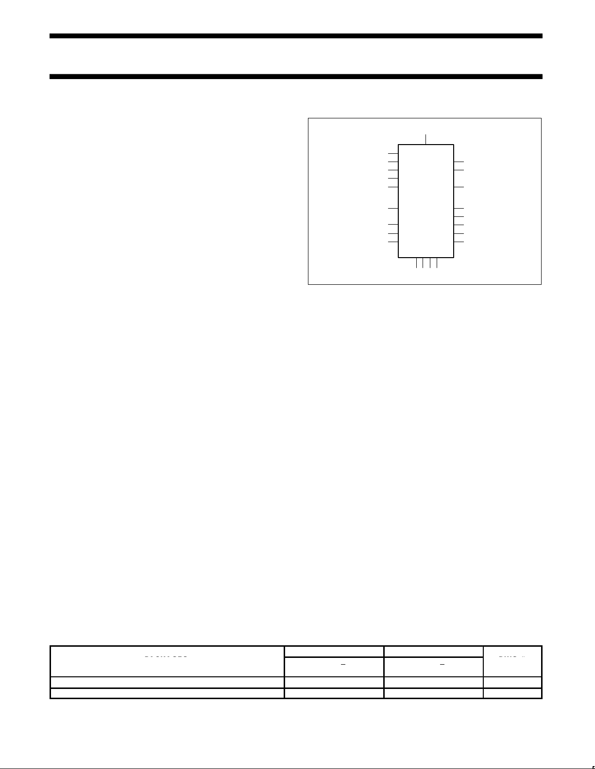
PIN CONFIGURATIONS
V
CC
A5:0
CEN
RDN
WRN
IACKN
RESET
X1/CLK
X2
RDa-d
V
SS
D7-0
DACKN
RQN
I/O0a–d
I/O1a–d
I/O2a–d
I/O3a–d
TDa-d
SD00178
•Programmable channel mode
– Normal (full-duplex), automatic echo, local loop back, remote
loopback
•Programmable interrupt priorities
•Identification of highest priority interrupt
•Global interrupt register set provides data from interrupting
channel
•Vectored interrupts with programmable vector format
•IACKN and DTACKN signals
•Built-in baud rate generator with choice of 18 rates
•Four I/O pins per UART for modem controls, clocks, etc.
•Power down mode
•High-speed CMOS technology
•52-pin PLCC and 48-pin DIP
•Commercial and industrial temperature ranges available
•On-chip crystal oscillator
•TTL compatible
•Single +5V power supply with low power mode
•Two multifunction programmable 16-bit counter/timers
•1MHz 16x mode operation
•30ns data bus release time
•“Watch Dog” timer for each receiver
ORDERING INFORMATION
COMMERCIAL INDUSTRIAL
PACKAGES
VCC = +5V +10%,
T
A
= 0oC to +70oC
VCC = +5V +10%,
T
A
= –40oC to +85oC
DWG #
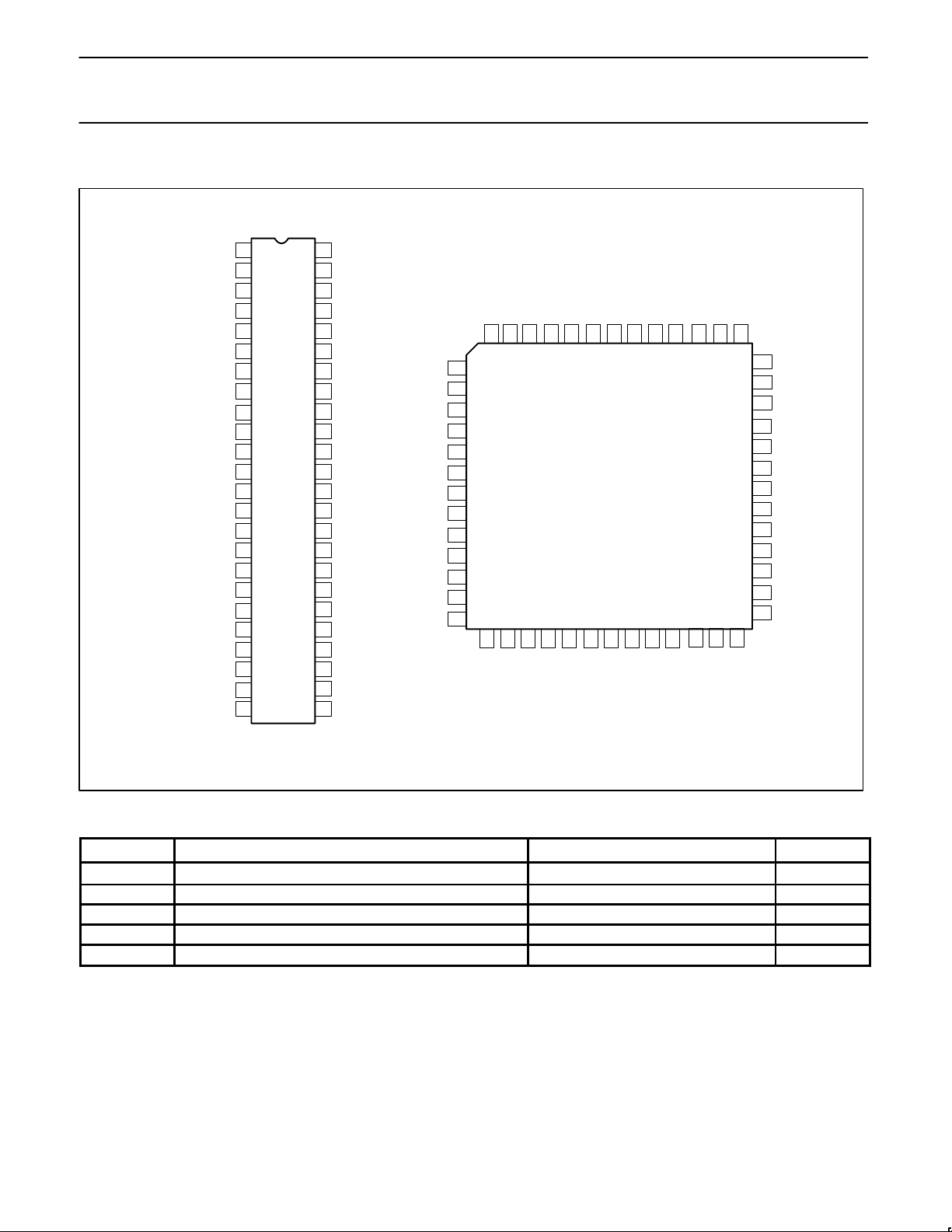
48-Pin Plastic Dual In-Line Package (DIP) SC68C94C1N SC68C94A1N SOT240-1
52-Pin Plastic Leaded Chip Carrier (PLCC) SC68C94C1A SC68C94A1A SOT238-3
Philips Semiconductors Product specification
SC68C94Quad universal asynchronous receiver/transmitter (QUART)
1995 May 1
2
PIN CONFIGURATIONS
46
45
44
48
47
46
45
44
43
42
41
40
39
38
37
36
35
34
33
32
31
30
29
1
2
3
4
5
6
7
8
9
10
11
12
13
14
15
16
17
18
19
20
28
27
26
25
21
22
23
24
X1/CLK
TXDD
RXDD
IRQN
A5
A4
A3
A2
A1
A0
WRN
CEN
RDN
DACKN
IACKN
TXDB
RXDB
D7
D6
D5
D4
D3
D1
D0
RXDA
TXDA
I/O2B
I/O1B
I/O0B
I/O2A
I/O1A
I/O0A
I/O0C
I/O1C
I/O2C
I/O0D
I/O1D
I/O2D
RXDC
TXDC
RESET
X2
V
SS
V
CC
D2
V
SS
V
SS
CEN
RDN
DACKN
IACKN
TXDB
RXDB
D7
D6
D5
D4
I/O3B
D1
D0
RXDA
TXDA
I/O2B
I/O1B
I/O0B
I/O3A
I/O2A
D2
V
SS
D3
I/O1A
A1
A2A3A4
A5
IRQN
RXDD
TXDD
X1/CLK
X2
TXDC
RXDC
I/O2D
I/O1D
I/O0D
I/O3C
I/O2C
I/O1C
I/O0C
RESET
I/O3D
I/O0A
V
SS
WRN
A0
48-Pin Dual-In-Line Package
52-Pin PLCC Package
1234
567
8
9
10
11
18
19
20
21 22 23 24 31 32 33
34
35
36
37
505152
38
39
40
41
42
43
25 26 27 28 29 30
12
13
14
15
16
17
474849
VSSV
CC
V
SS
V
SS
SD00179
ABSOLUTE MAXIMUM RATINGS
1, 2
SYMBOL
PARAMETER RATING UNIT
T
A
Operating ambient temperature range
3
Note 4
o
C
T
STG
Storage temperature range –65 to +150
o
C
V
CC
Voltage from V
DD
to GND
4
–0.5 to +7.0 V
V
S
Voltage from any pin to ground
4
–0.5 to V
CC
+0.5 V
P
D
Power dissipation 1
W
NOTES:
1. Stresses above those listed under Absolute Maximum Ratings may cause permanent damage to the device. This is a stress rating only and
functional operation of the device at these or any other condition above those indicated in the operation section of this specification is not
implied.
2. For operating at elevated temperatures, the device must be derated based on +150°C maximum junction temperature.
3. This product includes circuitry specifically designed for the protection of its internal devices from damaging effects of excessive static
charge. Nonetheless, it is suggested that conventional precautions be taken to avoid applying any voltages larger than the rated maxima.
4. Parameters are valid over specified temperature range. See ordering information table for applicable temperature range and operating
supply range.
Philips Semiconductors Product specification
SC68C94Quad universal asynchronous receiver/transmitter (QUART)
1995 May 1
3
BLOCK DIAGRAM
8
D0–D7
RDN
WRN
CEN
A0–A5
RESET
X1/CLK
X2
6
BUS BUFFER
OPERATION CONTROL
ADDRESS
DECODE
R/W CONTROL
TIMING
CHANNEL A
MR 0, 1, 2
CR
SR
INPUT PORT
OUTPUT PORT
OPCR
CSR Rx
CSR Tx
CRYSTAL
OSCILLATOR
POWER UP-DOWN
LOGIC
SAME AS
DUART AB
8 BYTE TRANSMIT
FIFO
TRANSMIT SHIFT
REGISTER
8 BYTE
RECEIVE FIFO
RECEIVE SHIFT
REGISTER
CHANGE-OF-
STATE
DETECTORS (4)
IPCR
ACR
FUNCTION SELECT
LOGIC
CHANNEL B
(AS ABOVE)
TIMING
CLOCK
SELECTORS
COUNTER/
TIMER
ACR
CTUR
CTLR
INTERRUPT CONTROL
IMR
ISR
INTERNAL DATA
BUS
TxDA
RxDA
TxDB
RxDB
1:0
4
TIMING
CONTROL
DACKN
DUART CD
TXDC
TXDD
RXDC
RXDD
I/O[3:0]C
I/O[3:0]D
1:0
I/O[3:0]B
I/O[3:0]A
•V
CC
•V
SS1
•V
SS2
•V
SS3
•V
SS4
BAUD RATE
GENERATOR
DUART AB
LOGIC
GLOBAL
REGISTERS
IRQN
IACKN
INTERRUPT ARBITRATION
8
DUART
COMMON
AB
18
4
4
4
÷ 2
SD00180
Philips Semiconductors Product specification
SC68C94Quad universal asynchronous receiver/transmitter (QUART)
1995 May 1
4
PIN DESCRIPTION
MNEMONIC TYPE NAME AND FUNCTION
CEN I Chip Select: Active low input that, in conjunction with RDN or WRN, indicates that the host MPU is trying to
access a QUART register. CEN must be inactive when IACKN is asserted.
A5:0 I Address Lines: These inputs select a 68C94 register to be read or written by the host MPU.
D7:0 I/O 8-bit Bidirectional Data Bus: Used by the host MPU to read and write 68C94 registers.
RDN I Read Strobe: Active low input. When this line is asserted simultaneously with CEN, the 68C94 places the
contents of the register selected by A5:0 on the D7:0 lines.
WRN I Write Strobe: Active low input. When this line is asserted simultaneously with CEN, the 68C94 writes the data
on D7:0 into the register selected by A5:0.
DACKN O Data ACKnowledge: Active low, open-drain output to the host MPU, which is asserted subsequent to a read or
write operation. For a read operation, assertion of DACKN indicates that register data is valid on D7:0. For a
write operation, it indicates that the data on D7:0 has been captured into the indicated register. This signal
corresponds to READYN on 80x86 processors and DTACKN on 680x0 processors.
IRQN O Interrupt Request: This active low open-drain output to the host MPU indicating that one or more of the
enabled UART interrupt sources has reached an interrupt value which exceeds that pre-programmed by host
software. The IRQN can be used directly as a 680x0 processor input; it must be inverted for use as an 80x86
interrupt input. This signal requires an external pull-up resistor.
IACKN I Interrupt ACKnowledge: Active low input indicates host MPU is acknowledging an interrupt requested. The
68C94 responds by placing an interrupt vector or interrupt vector modified on D7-D0 and asserting DACKN. This
signal updates the CIR register in the interrupt logic. CEN must be high during this cycle.
TDa-d O Transmit Data: Serial outputs from the four UARTs.
RDa-d I Receive Data: Serial inputs to the four UARTs/
I/O0a-d I/O Input/Output 0: A multi-use input or output signal for each UART. These pins can be used as general purpose
inputs, Clear to Send inputs, 1X or 16X Transmit Clock outputs or general purpose outputs. Change-of-state
detection is provided for these pins.
I/O1a-d I/O Input/Output 1: A multi-use input or output signal for each UART. These pins can be used as general purpose
or 1X or 16X transmit clock inputs, or general purpose 1X or 16X receive clock outputs. Change-of-state
detection is provided for these pins. In addition, I/O1a and I/O1c can be used as Counter/Timer inputs and I/O1b
and I/O1d can be used as Counter/Timer outputs.
I/O2a-d I/O Input/Output 2: A multi-use input or output signal for each UART. These pins can be used as general purpose
inputs, 1X or 16X receive clock inputs, general purpose outputs, RTS output or 1X or 16X receive clock outputs.
I/O3a-d I/O Input/Output 3: A multi-use input or output signal for each UART. These pins can be used as general purpose
inputs, 1X or 16X transmit clock inputs, general purpose outputs, or 1X or 16X transmit clock outputs.
RESET I Master Reset: Active high reset for the 68C94 logic. Must be asserted at power-up, may be asserted at other
times that the system is to be reset and restarted. OSC set to divide by 1, MR pointer set to 1, DACKN enabled,
I/O pins to input. Registers reset: OPR, CIR. IRQN, DTACKN, IVR Interrupt Vector, Power Down, Test registers,
FIFO pointers, Baud rate generator, Error Status, Watch Dog Timers, Change of State detectors, counter/timer to
timer, Transmitter and Receiver controllers and all interrupt bits. If reset pin is not used, then first chip access
should be to celar ‘power-down’ mode.
X1/CLK I Crystal 1 or Communication Clock: This pin is normally connected to one side of a 3.6864MHz or a
7.3728MHz crystal, or can be connected to an external clock up to 8MHz.
X2 O Crystal 2: If a crystal is used, this pin should be connected to its other terminal. If an external clock is applied to
X1, this pin should be left unconnected.
VCC, V
SS
Power and grounds: respectively.
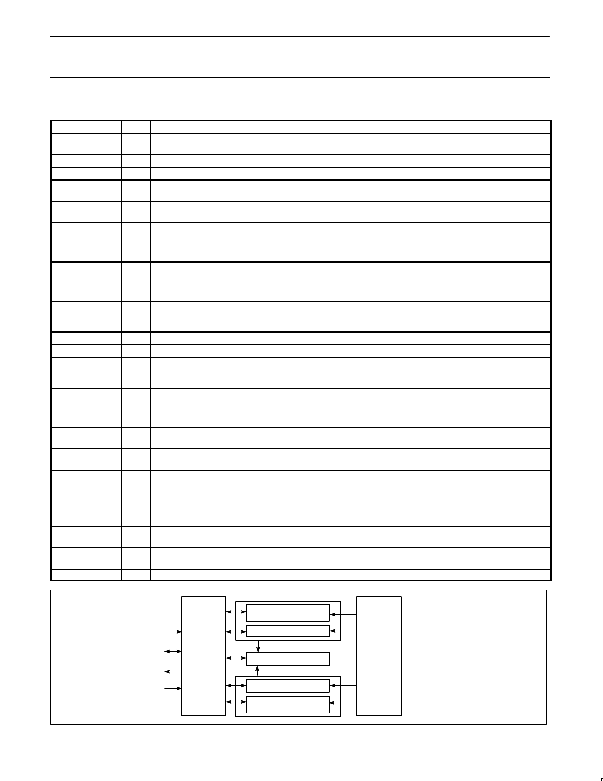
COUNTER/TIMER
I/O PORT CONTROL
UARTS A/B
INTERRUPT CONTROL
BLOCK B
UARTS C/D
I/O CONTROL
I/O PORT CONTROL
A0-A5
D (7:0)
DTACKN
IACKN
BAUD
RATE
GENERATOR
BUS
INTERFACE
BLOCK A
SD00161
Figure 1. Channel Architecture

Philips Semiconductors Product specification
SC68C94Quad universal asynchronous receiver/transmitter (QUART)
1995 May 1
5
Table 1. QUART Registers
1
A5:0
READ (RDN = Low) WRITE (WRN = Low)
000000 Mode Register a (MR0a, MR1a, MR2a) Mode Register a (MR0a, MR1a, MR2a)
000001 Status Register a (SRa) Clock Select Register a (CSRa)
000010 Reserved Command Register a (CRa)
000011 Receive Holding Register a (RxFIFOa) Transmit Holding Register a (TxFIFOa)
000100 Input Port Change Reg ab (IPCRab) Auxiliary Control Reg ab (ACRab)
000101 Interrupt Status Reg ab (ISRab) Interrupt Mask Reg ab (IMRab)
000110 Counter/Timer Upper ab (CTUab) Counter/Timer Upper Reg ab (CTURab)
000111 Counter/Timer Lower ab (CTLab) Counter/Timer Lower Reg ab (CTLRab)
001000 Mode Register b (MR0b, MR1b, MR2b) Mode Register b (MR0b, MR1b, MR2b)
001001 Status Register b (SRb) Clock Select Register b (CSRb)
001010 Reserved Command Register b (CRb)
001011 Receive Holding Register b (RxFIFOb) Transmit Holding Register b (TxFIFOb)
001100 Output Port Register ab (OPRab) Output Port Register ab (OPRab)
001101 Input Port Register ab (IPRab) I/OPCRa (I/O Port Control Reg a)
001110 Start Counter ab I/OPCRb (I/O Port Control Reg b)
001111 Stop Counter ab Reserved
010000 Mode Register c (MR0c, MR1c, MR2c) Mode Register c (MR0c, MR1c, MR2c)
010001 Status Register c (SRc) Clock Select Register c (CSRc)
010010 Reserved Command Register c (CRc)
010011 Receive Holding Register c (RxFIFOc) Transmit Holding Register c (TxFIFOc)
010100 Input Port Change Reg cd (IPCRcd) Auxiliary Control Reg cd (ACRcd)
010101 Interrupt Status Reg cd (ISRcd) Interrupt Mask Reg cd (IMRcd)
010110 Counter/Timer Upper cd (CTUcd) Counter/Timer Upper Reg cd (CTURcd)
010111 Counter/Timer Lower cd (CTLcd) Counter/Timer Lower Reg cd (CTLRcd)
011000 Mode Register d (MR0d, MR1d, MR2d) Mode Register d (MR0d, MR1d, MR2d)
011001 Status Register d (SRd) Clock Select Register d (CSRd)
011010 Reserved Command Register d (CRd)
011011 Receive Holding Register d (RxFIFOd) Transmit Holding Register d (TxFIFOd)
011100 Output Port Register cd (OPRcd) Output Port Register cd (OPRcd)
011101 Input Port Register cd (IPRcd) I/OPCRc (I/O Port Control Reg c)
011110 Start Counter cd I/OPCRd (I/O Port Control Reg d)
011111 Stop Counter cd Reserved
100000 Bidding Control Register a (BCRa) Bidding Control Register a (BCRa)
100001 Bidding Control Register b (BCRb) Bidding Control Register b (BCRb)
100010 Bidding Control Register c (BCRc) Bidding Control Register c (BCRc)
100011 Bidding Control Register d (BCRd) Bidding Control Register d (BCRd)
100100 Reserved Power Down
100101 Reserved Power Up
100110 Reserved Disable DACKN
100111 Reserved Enable DACKN
101000 Current Interrupt Register (CIR) Reserved
101001 Global Interrupting Channel Reg (GICR) Interrupt Vector Register (IVR)
101010 Global Int Byte Count Reg (GIBCR) Update CIR
101011 Global Receive Holding Reg (GRxFIFO) Global Transmit Holding Reg (GTxFIFO)
101100 Interrupt Control Register (ICR) Interrupt Control Register (ICR)
101101 Reserved BRG Rate. 00 = low; 01 = high
101110 Reserved Set X1/CLK divide by two
2
101111 Reserved Set X1/CLK Normal
2
110000–111000 Reserved Reserved
111001 Test Mode Test Mode
111010–111111 Reserved Reserved
NOTES:
1. Registers not explicitly reset by hardware reset power up randomly.
2. In X1/CLK divide by 2 all circuits receive the divided clock except the BRG and change-of-state detectors.

Philips Semiconductors Product specification
SC68C94Quad universal asynchronous receiver/transmitter (QUART)
1995 May 1
6
FUNCTIONAL BLOCKS
The QUART is composed of four Philips Semiconductors
industry–standard UARTs, each having a separate transmit and
receive channel.
The Basic UART cells in the QUART are configured with 8-byte
Receive FIFOs and 8-byte Transmit FIFOs. Hardware supports
interrupt priority arbitration based on the number of bytes available
in the transmit and receive FIFOs, counter/timers, change of state
detectors, break detect or receiver error. Attempts to push a full
FIFO or pop an empty FIFO do not affect the count.
Baud Rate Generator
The baud rate generator used in the QUART is the same as that
used in other Philips Semiconductors industry standard UARTs. It
provides 18 basic Baud rates from 50 baud to 38,400 baud. It has
been enhanced to provide to provide other baud rates up to 230,400
baud based on a 3.6364MHz clock; with an 8.0MHz clock rates to
500K baud. Other rates are available by setting the BRG rate to high
at address 2D hex or setting Test 1 on at address 39 hex. See Table
3. These two modes are controlled by writing 00 or 01 to the
addresses above. They are both set to 00 on reset. External Rx and
Tx clocks yield rates to 1MHz in the 16X mode.
BLOCK DIAGRAM
As shown in the block diagram, the QUART consists of: data bus
buffer, interrupt control, operation control, timing, and four receiver
and transmitter channels. The four channels are divided into two
different blocks, each block independent of the other .
Channel Blocks
There are two blocks (Block Diagram), each containing two sets of
receiver/transmitters. In the following discussion, the description
applies to Block A which contains channels a and b. However, the
same information applies to all channel blocks.
Data Bus Buffer
The data bus buffer provides the interface between the external and
internal data buses. It is controlled by the operation control block to
allow read and write operations to take place between the controlling
CPU and the QUART.
Operation Control
The operation control logic receives operation commands from the
CPU and generates appropriate signals to internal sections to
control device operation. It contains address decoding and read and
write circuits to permit communications with the microprocessor via
the data bus buffer. The functions performed by the CPU read and
write operations are shown in Table 1.
Mode registers (MR) 0, 1 and 2 are accessed via an address
counter. This counter is set to one (1) by reset or a command 1x to
the Command Register for compatibility with other Philips
Semiconductors software. It is set to 0 via a command Bx to the
Command Register (CR). The address counter is incremented with
each access to the MR until it reaches 2 at which time it remains at
2. All subsequent accesses to the MR will be to MR2 until the MR
counter is changed by a reset or an MR counter command.
The Mode Registers control the basic configuration of the UART
channels. There is one for each UART. (Transmitter/receiver pair)
Timing Circuits
The timing block consists of a crystal oscillator, a baud rate
generator, power up/down logic and a divide by 2 selector. Closely
associated with the timing block are two 16-bit counter/timers; one
for each DUART.
Oscillator
The crystal oscillator operates directly from a 3.6864MHz crystal
connected across the X1/ CLK and X2 inputs with a minimum of
external components. If an external clock of the appropriate
frequency is available, it may be connected to X1/CLK. If an external
clock is used instead of a crystal, X1 must be driven and X2 left
floating as shown in Figure 10. The clock serves as the basic timing
reference for the baud rate generator (BRG), the counter/timer, and
other internal circuits. A clock frequency, within the limits specified in
the electrical specifications, must be supplied even if the internal
BRG is not used.
The X1 pin always supplies the clock for the baud rate generator.
The X1 pin also has a feature such that it may be divided by 2. The
divide by two mode must always be used whenever the X1 pin is
above 4MHz. The baud rate generator supplies the standard rates
when X1 is at 3.6864MHz. In the divide by 2 mode, all circuits
receive the divide by two clock except baud rate generator and I/O
pin change-of-state detectors. 7.3738MHz clock doubles standard
baud rates.
Baud Rate Generator
The baud rate generator operates from the oscillator or external
clock input and is capable of generating 18 commonly used data
communications baud rates ranging from 50 to 38.4K baud. The
eighteen BRG rates are grouped in two groups. Eight of the 18 are
common to each group. The group selection is controlled by ACR[7].
See the Baud Rate Table 3. The clock outputs from the BRG are at
16X the actual baud rate. The counter/timer can be used as a timer
to produce a 16X clock for any other baud rate by counting down the
crystal clock or an external clock. The clock selectors allow the
independent selection, by the receiver and transmitter, of any of
these baud rates or an external timing signal.
Counter/Timer
The counter timer is a 16-bit programmable divider that operates in
one of three modes: counter, timer, time out. In the timer mode it
generates a square wave. In the counter mode it generates a time
delay. In the time out mode it monitors the time between received
characters. The C/T uses the numbers loaded into the
Counter/Timer Lower Register (CTLR) and the Counter/T imer Upper
Register (CTUR) as its divisor.
There are two counter/timers in the QUART; one for each block.
The counter/timer clock source and mode of operation (counter or
timer) is selected by the Auxiliary Control Register bits 6 to 4
(ACR[6:4]). The output of the counter/timer may be used for a baud
rate and/or may be output to the I/O pins for some external function
that may be totally unrelated to data transmission. The
counter/timer also sets the counter/timer ready bit in the Interrupt
Status Register (ISR) when its output transitions from 1 to 0.
A register read address (see Table 1) is reserved to issue a start
counter/timer command and a second register read address is
reserved to issue a stop command. The value of D(7:0) is ignored.
The START command always loads the contents of CTUR, CTLR to
the counting registers. The STOP command always resets the
ISR(3) bit in the interrupt status register.
Timer Mode
In the timer mode a symmetrical square wave is generated whose
half period
is equal in time to division of the selected counter/timer
clock frequency by the 16-bit number loaded in the CTLR CTUR.
Thus, the frequency of the counter/timer output will be equal to the
counter/timer clock frequency divided by twice the value of the
CTUR CTLR. While in the timer mode the ISR bit 3 (ISR[3]) will be

Philips Semiconductors Product specification
SC68C94Quad universal asynchronous receiver/transmitter (QUART)
1995 May 1
7
set each time the counter/timer transitions from 1 to 0. (High to low)
This continues regardless of issuance of the stop counter command.
ISR[3] is reset by the stop counter command. NOTE: Reading of
the CTU and CTL registers in the timer mode is not meaningful.
When the C/T is used to generate a baud rate
and
the C/T is
selected through the CSR then the receivers and/or transmitter will
be operating in the 16x mode. Calculation for the number ‘n’ to
program the counter timer upper and lower registers is shown below.
n=2 x 16 x Baud rate desired/(C/T Clock Frequency
Often this division will result in a non-integer number; 26.3 for
example. One can only program integer numbers to a digital divider.
Therefore 26 would be chosen. This gives a baud rate error of
0.3/26.3 which is 1.14%; well within the ability of the asynchronous
mode of operation.
Counter Mode
In the counter mode the counter/timer counts the value of the CTLR
CTUR down to zero and then sets the ISR[3] bit and sets the
counter/timer output from 1 to 0. It then rolls over to 65,365 and
continues counting with no further observable effect.
Reading the C/T in the counter mode outputs the present state of
the C/T. If the C/T is not stopped, a read of the C/T may result in
changing data on the data bus.
Timeout Mode
The timeout mode uses the received data stream to control the
counter.The time-out mode forces the C/T into the timer mode.
Each time a received character is transferred from the shift register
to the RxFIFO, the counter is restarted. If a new character is not
received before the counter reaches zero count, the counter ready
bit is set, and an interrupt can be generated. This mode can be used
to indicate when data has been left in the Rx FIFO for more than the
programmed time limit. If the receiver has been programmed to
interrupt the CPU when the receive FIFO is full, and the message
ends before the FIFO is full, the CPU will not be interrupted for the
remaining characters in the RxFIFO.
By programming the C/T such that it would time out in just over one
character time, the above situation could be avoided. The
processor would be interrupted any time the data stream had
stopped for more than one character time. NOTE: This is very
similar to the watch dog time of MR0. The difference is in the
programmability of the delay time and that the watchdog timer is
restarted by either a receiver load to the RxFIFO or a system read
from it.
This mode is enabled by writing the appropriate command to the
command register. Writing an ‘Ax’ to CRA or CRB will invoke the
timeout mode for that channel. Writing a ‘Cx’ to CRA or CRB will
disable the timeout mode. Only one receiver should use this mode
at a time. However, if both are on, the timeout occurs after both
receivers have been inactive for the timeout period. The start of the
C/T will be on the logical or of the two receivers.
The timeout mode disables the regular START/STOP counter
commands and puts the C/T into counter mode under the control of
the received data stream. Each time a received character is
transferred from the shift register to the RxFIFO, the C/T is stopped
after one C/T clock, reloaded with the value in CTUR and CTLR and
then restarted on the next C/T clock. If the C/T is allowed to end the
count before a new character has been received, the counter ready
bit, ISR[3], will be set. If IMR[3] is set, this will generate an interrupt.
Since receiving a character restarts the C/T, the receipt of a
character after the C/T has timed out will clear the counter ready bit,
ISR[3], and the interrupt. Invoking the ‘Set Timeout Mode On’
command, CRx=‘Ax’, will also clear the counter ready bit and stop
the counter until the next character is received.
The counter timer is controlled with six commands: Start/Stop C/T,
Read/Write Counter/Timer lower register and Read/W rite
Counter/Timer upper register. These commands have slight
differences depending on the mode of operation. Please see the
detail of the commands under the CTLR CTUR Register
descriptions.
Time Out Mode Caution
When operating in the special time out mode, it is possible to
generate what appears to be a “false interrupt”, i.e., an interrupt
without a cause. This may result when a time-out interrupt occurs
and then, BEFORE the interrupt is serviced, another character is
received, i.e., the data stream has started again. (The interrupt
latency is longer than the pause in the data strea.) In this case,
when a new character has been receiver, the counter/timer will be
restarted by the receiver, thereby withdrawing its interrupt. If, at this
time, the interrupt service begins for the previously seen interrupt, a
read of the ISR will show the “Counter Ready” bit not set. If nothing
else is interrupting, this read of the ISR will return a x’00 character.
Receiver and Transmitter
The QUART has four full-duplex asynchronous
receiver/transmitters. The operating frequency for the receiver and
transmitter can be selected independently from the baud rate
generator, the counter/timer, or from an external input.
Registers associated with the communications channel are the
mode registers (MR0, MR1 and MR2) Clock Select Register (CSR),
Command Register (CR), Status Register (SR), Transmit FIFO
(TxFIFO), and the Receive FIFO (RxFIFO). The transmit and
receive FIFOs are each eight characters deep. The receive FIFO
also stores three status bits with each character.
Transmitter
The transmitter accepts parallel data from the CPU and converts it
to a serial bit stream on the TxD output pin. It automatically sends a
start bit followed by the programmed number of data bits, an
optional parity bit, and the programmed number of stop bits. The
least significant bit is sent first. Following the transmission of the
stop bits, if a new character is not available in the TxFIFO, the TxD
output remains high and the TxEMT bit in the SR will be set to 1.
Transmission resumes and the TxEMT bit is cleared when the CPU
loads a new character in the TxFIFO. In the 16X clock mode, this
also re-synchronizes the internal 1X transmitter clock so that
transmission of the new character begins with minimum delay.
If the transmitter is disabled it continues operating until the character
currently being transmitted and any characters in the TxFIFO,
including parity and stop bits, have been transmitted. New data
cannot be loaded to the TxFIFO when the transmitter is disabled.
The transmitter can be forced to send a break (a continuous low
condition) by issuing a START BREAK command via the CR
register. The break is terminated by a ST OP BREAK command or a
transmitter reset..
TxFIFO
The TxFIFO empty positions are encoded as a three bit number for
presentation to the bidding logic. The coding will equal the number
of bytes that remain to be filled. That is, a binary number of 101 will
mean five bytes may be loaded; 111 means 7, etc. Eight positions
will be indicated by a binary 111
and
the FIFO empty bit will be set.
Receiver
The receiver accepts serial data on the RxD pin, converts the serial
input to parallel format, checks for start bit, stop bit, parity bit (if any),

Philips Semiconductors Product specification
SC68C94Quad universal asynchronous receiver/transmitter (QUART)
1995 May 1
8
or break condition, and presents the assembled character to the
CPU via the receiver FIFO.
The receiver operates in two modes: the 1X and 16X. The 16X
mode is the more robust of the two. It allows the receiver to
establish a phase relation to the remote transmitter clock within 1/16
of a bit time and also allows validation of the start bit. The 1X mode
does not validate the start bit and assumes that the receiver clock
rising edge is centered in the data bit cell. The use of the 1X mode
implies that the transmitter clock is available to the receiver.
When operating in the 16X mode and after the receiver has been
enabled the receiver state machine will look for a high to low
transition on the RxD input. The detection of this transition will cause
the divider being driven by the 16X clock to be reset to zero and
continue counting. When the counter reaches 7 the RxD input is
sampled again and if still low a valid START BIT will be detected. If
the RxD input is high at count 7 then an invalid start bit will have
been sensed and the receiver will then look for another high to low
transition and begin validating again.
When a valid start bit is detected the receiver state machine allows
the 16X divider circuit to continue counting 0 to 15. Each time the
receiver passes count 7 (the theoretical center of the bit time)
another data bit is clocked into the receiver shift register until the
proper number of bits have been received including the parity bit, if
used, and 1/2 stop bit. After the STOP BIT is detected the receiver
state machine will wait until the next falling edge of the 1X clock and
then clock the assembled character and its status bits into the
receiver FIFO on the next rising edge of the 1X clock. The delay
from the detection of the STOP BIT to the loading of the character to
the RxFIFO will be from one half to one and one half X1 clock
periods, or twice that if X1/2 is used. Receiver Status Register bits
for FIFO READY, FIFO FULL, parity error, framing error, break
detect will also set at this time. The most significant bits for data
characters less than eight bits will be set to zero.
After the stop bit is detected, the receiver will immediately look for
the next start bit. However, if a non-zero character was received
without a stop bit (i.e. framing error) and RxD remains low for
one-half of the bit period after the stop bit was sampled, then the
receiver operates as if a new start bit transition had been detected at
that point (one-half bit time after the stop bit was sampled). The
parity error, framing error and overrun error (if any) are strobed into
the SR at the received character boundary, before the RxRDY
status bit is set.
If a break condition is detected (RxD is low for the entire character
including the stop bit), only one character consisting of all zeros will
be loaded in the FIFO and the received break bit in the SR is set to
1. The “Change of Break” bit in the ISR at position 2 or 6 is also set
at this time. Note that the “Change of Break” bit will set again when
the break condition terminates. The RxD input must return to high
for two (2) clock edges of the X1 crystal clock for the receiver to
recognize the end of the break condition and begin the search for a
start bit. This will usually require a high time of one X1 clock
period or 3 X1 edges since the clock of the controller is not
synchronous to the X1 clock.
NOTE: If the RxD input is low when the receiver is enabled and
remains low for at least 9/16 of a bit time a valid start bit will be
seen and data (probably random) will be clocked into the
receiver FIFO. If the line remains low for a full character time
plus a stop bit then a break will be detected.
Each receiver is equipped with a watchdog timer. This timer is
enabled by MR0[7] and counts 64 RxC1X clocks. Its purpose is to
alert the controlling CPU that data is in the FIFO which has not been
read. This situation may occur at the end of a message when the
last group of characters was not long enough to cause an interrupt.
RECEIVER FIFO
The RxFIFO consists of a first-in-first-out (FIFO) with a capacity of
eight characters. Data is loaded from the receive shift register into
the top-most empty position of the FIFO. The RxRDY bit in the
status register (SR) is set whenever one or more characters are
available to be read; a FFULL status bit is set if all eight stack
positions are filled with data. The number of filled positions is
encoded into a 3-bit value. This value is sent to the interrupt bidding
logic where it is used to generate an interrupt. A read of the RxFIFO,
outputs the data at the top of the FIFO. After the read cycle, the data
FIFO and its associated status bits are ‘popped’ thus emptying a
FIFO position for new data.
NOTE: The number of filled positions in the RxFIFO is coded
as actual number filled positions. Seven filled will be coded as
7. Eight filled positions will be coded as 7
and
the RxFIFO full
status bit will be set.
In addition to the data word, three status bits (parity error, framing
error, and received break) are appended to each data character in
the FIFO. Status can be provided in two ways, as programmed by
the error mode control bit in the mode register. In the ‘character’
mode, status is provided on a character-by-character basis: the
status applies only to the character at the top of the FIFO. In the
‘block’ mode, the status provided in the SR for these three bits is the
logical OR of the status for all characters coming to the top of the
FIFO since the last reset error command was issued. In either
mode, reading the SR does not affect the FIFO. The FIFO is
‘popped’ only when the RxFIFO is read. Therefore, the SR should
be read prior to reading the corresponding data character.
If the FIFO is full when a new character is received, that character is
held in the receive shift register until a FIFO position is available. If
an additional character is received while this state exists, the
contents of the FIFO are not affected: the character previously in the
shift register is lost and the overrun error status bit, SR[4], will be set
upon receipt of the start bit of the new (overrunning) character.
Watchdog Timer
A “watchdog” timer is associated with each receiver. Its interrupt is
enabled by MR0[7]. The purpose of this timer is alerting the control
processor that characters are in the RxFIFO which have not been
read and/or the datastream has stopped. This situation may occur
at the end of a transmission when the last few characters received
are not sufficient to cause an interrupt.
This counter times out after 64 bit times. It is reset each time a
character is transferred from the Receive shift register to the
RxFIFO or a read of the RxFIFO is executed.
WAKE-UP MODE (MULTI-DROP OR 9-BIT)
In addition to the normal transmitter and receiver operation
described above, the QUART incorporates a special mode which
provides automatic “wakeup” of a receiver through address frame
(or character) recognition for multi-processor or multi-station
communications. This mode is selected by programming MR1[4:3]
to ‘11’.
In this mode of operation a ‘master’ station transmits an address
character to the several ‘slave’ stations on the line. The address
character is identified by setting its parity bit to 1. The slave stations
will usually have their receivers partially enabled as a result of
setting MR1[4:3] to 11. When the receiver sees a one in the parity
position, it considers it an address bit and loads that character to the
RxFIFO and set the RxRDY bit in the status register. The user
would usually set the receiver interrupt to occur on RxRDY as well.
(All characters whose parity bits are set to 0 will be ignored). The
local processor at the slave station will read the ‘address’ character
just received. The local processor will test for an address match for

Philips Semiconductors Product specification
SC68C94Quad universal asynchronous receiver/transmitter (QUART)
1995 May 1
9
this station and if match occurs it will enable the local receiver and
receive the following data characters. The master will normally
follow an address character(s) with data characters. Since the data
characters transmitted by the master will have their parity bits set to
zero, stations other than the addressed one(s) will ignore the data.
NOTE: The time between address and data fields must be
enough for the local processor to test the address character
and enable the receiver. At bit times approaching 10µs this may
begin to be a point of concern.
The parity (Address/Data) bit should not be changed until the last
stop bit of an address has been sent. Similarly the A/D bit should
not be changed to address until the last stop bit has been sent.
Either of these conditions will be indicated by an active TxEMT bit in
the SR.
The parity bit is not part of the TxFIFO. It is in the transmitter state
machine. However, it could be controlled in the FIFO if 5, 6 or 7 bit
data was transmitted by using a 6, 7 or 8 bit character. The most
significant bit would then be in the ‘parity’ position and represent the
A/D bit. The design of the UART is based, however, on the A/D bit
being controlled from the MR register.
Parity should be changed immediately before the data bytes
will be loaded to the transmitter.
A transmitted character consists of a start bit, the programmed
number of data and stop bits and an “address/data” bit. The parity
bit is used as the address or data indicator. The polarity of the A/D
bit is selected by setting MR1[2] to zero or one; zero indicates that
the current byte is data, while one indicates that the current byte is
addressed. The desired polarity of the A/D bit (parity) should be
programmed before
the TxFIFO is loaded.
The receiver should be enabled before the beginning of the first data
bit. The time required is dependent on the interrupt latency of the
slave receivers. The transmitter is able to start data immediately
after the address byte has been sent.
While in this mode, the receiver continuously looks at the received
data stream, whether it is enabled or disabled. If disabled, it sets the
RxRDY status bit and loads the character in the RxFIFO if the
received A/D bit is a one, but discards the received character if the
received A/D bit is a zero. If enabled, all received characters are
then transferred to the CPU via the RxFIFO. In either case, the data
bits are loaded in the data FIFO while the A/D bit is loaded in the
status FIFO position normally used for parity error (SR[5]). Framing
error, overrun error, and break detect operate normally whether or
not the receiver is enabled.
INPUT OUTPUT (I/O) PINS
There are 16 multi-use pins; four for each UART. These pins are
accessed and controlled via the Input Port Register (IPR), I/O Port
Control Register (I/OPCR), Input Port Change Register (IPCR), and
Output Port Register (OPR). They may be individually programmed
to be inputs or outputs. See Table 5.
I/O0x and I/O1x pins have change of state detectors. The change of
state detectors sample the input ports every 26.04µs (with the X1
clock at 3.686400MHz) and set the change bit in the IPCR if the pin
has changed since it was last read. Whether the pins are
programmed as inputs or outputs the change detectors still operate
and report changes accordingly. See the register descriptions of the
I/O ports for the detailed use of these features.
A read of the IPCR resets the I/O COS (change Of State) detectors.
Interrupt Priority System
The interrupt control for the QUART has been designed to provide
very low interrupt service overhead for the controlling processor
while maintaining a high degree of flexibility in setting the
importance of interrupts generated in different functional blocks of
the device.
This is accomplished by allowing each function of the QUART (18
total) which may cause an interrupt to generate a variable numeric
code which contains the identity of the source, channel number and
severity level. This code is compared (at the X1 clock rate or the X1
clock rate divided by 2) to an interrupt threshold. When the interrupting source generates a code that is numerically greater than the
interrupt threshold the IRQN is asserted
This is referred to as the bidding process. The winning bid contains,
in different fields, all the characteristics of the winning bidder. This
data may be used in several ways to steer the controlling processor
to the proper type and amount of service required (usually the
amount of service refers to the number of bytes written to the transmitter or read from the receiver). Access to the winning bidder is
provided via the CIR (Current Interrupt Register), interrupt vectors,
modified interrupt vectors and Global registers.
NOTE: IRQN is essentially a level output. It will go active on an
interrupt condition and stays active until all interrupting sources are
serviced.
IRQN is designed to be an open drain active low level output. It will
go low under the control of the arbitration system and remain low
until the arbitration has determined that no more sources require
service.
When only one Rx or Tx is interrupting, it is possible to see the
IRQN assert more than once if, during an access to the FIFO, the
CEN input is inactive for more than two cycles of the X1 clock or X1
divide by 2 if that feature is enabled.
IACKN may be thought of as a special read input. Driving IACKN
low will update the CIR and then read the Interrupt Vector Register
or the Interrupt Vector Register modified by the CIR.
Functional Description of the Interrupt Arbitration
For the purpose of this description, a ‘source’ is any one of the 18
QUART circuits that may generate an interrupt. The QUART
contains eighteen sources which may cause an interrupt:
1. Four receiver data FIFO filled functions.
2. Four receiver BREAK detect functions.
3. Four transmitter FIFO space available functions.
4. Four “Change of State” detectors.
5. Two counter/timers.
The interrupt logic at each source produces a numeric code that
identifies its interrupt priority condition currently pending. This code
is compared to a programmable Interrupt Threshold via the
arbitration logic which determines if the IRQN should be asserted.
The arbitration logic only judges those possible interrupt sources
which have been allowed to bid via the IMR (Interrupt Mask
Register).
The arbitration logic produces a value which is the concatenation of
the channel number, interrupt type, FIFO fill level and user-defined
fields. The channel number and interrupt type fields are hardwired.
During the “bid arbitration” process all bids from enabled sources
are presented, simultaneously, to an internal interrupt bus. The
bidding system and formats are discussed in more detail in
following sections.
The interrupt arbitration logic insures that the interrupt with the
numerically largest bid value will be the only source driving the
interrupt bus at the end of the arbitration period. The arbitration

Philips Semiconductors Product specification
SC68C94Quad universal asynchronous receiver/transmitter (QUART)
1995 May 1
10
period follows the period of the X1 clock. The maximum speed is
4.0MHz. If a higher speed X1 clock is used then the X1 clock “divide
by 2” feature must be used.
The value of the winning bid determined during the arbitration cycle
is compared to the “Interrupt Threshold” contained in the ICR
(Interrupt Control Register). If the winning bid exceeds the value of
the ICR the IRQN is asserted.
Priority Arbitration and Bidding
Each of the five “types” of interrupts has slightly different “bid” value,
as follows:
Receivers
Transmitters
Break Detect
Change of State
Counter/Timer
# rcv’d rEr 1 1 Chan #
3 1 1 1 2
0 # avail 1 0 Chan #
1 3 1 1 2
Programmable 1 0 0 Chan #
3 1 1 1 2
Programmable 0 0 1 Chan #
3 1 1 1 2
Programmable 1 0 1 Chan #
2 1 1 1 2
0
1
SD00162
Bits shown above as ‘0’ or ‘1’ are hard-wired inputs to the arbitration
logic. Their presence allows determination of the interrupt type and
they insure that no bid will have a value of all zeros (a condition that
is indistinguishable from not bidding at all). They also serve to set a
default priority among the non-receive/transmit types when the
programmable fields are all zeros.
The channel number always occupies the two LSBs. Inclusion of
the channel number insures that a bid value generated will be
unique and that a single “winner” will drive the Interrupt Bus at the
end of the arbitration interval. The channel number portion of each
UARTs bid is hard-wired with UARTa being channel number 0 and
so forth.
As can be seen above, bits 4:2 of the winning bid value can be used
to identify the type of interrupt, including whether data was received
correctly or not. Like the Channel number field, these bits are
hard-wired for each interrupt source.
The “# rcv’d” and “# avail” fields indicate the number of bytes
present in the receiver FIFO and the number of empty bytes in the
transmitter FIFO, respectively.
NOTE: When there are zero bytes in the receiver’s FIFO, it does
NOT bid. Similarly, a full transmitter FIFO makes NO bid. In the
case where all bids have been disabled by the Interrupt Mask
Register or as a result of their byte counts, the active-low Interrupt
Bus will return FFh. This value always indicates no interrupt source
is active and IRQN will be negated.
The high order bit of the transmitter “bid” is always zero. An empty
transmit FIFO is, therefore, fixed at a lower interrupt priority than a
1/2 full receive FIFO. Bit 4 of a receiver bid is the Receiver Error Bit
(RER). The RER is the OR of the parity, framing and overrun error
conditions. The RER does little to modify the priority of receiver
interrupts vs. transmitter interrupts. It is output to the Interrupt Bus
to allow inclusion of good data vs. problem data information in the
Current Interrupt Register.
The high order bits of bids for received break, CoS (Change of
State) and Counter/Timer events are all programmable. By
programming ones in these fields, the associated interrupt source
can be made more significant than most receiver and all transmitter
interrupts. Values near zero in these fields makes them lower
priority classes of interrupt.
The channel address for C/T ab will be encoded as channel B (01)
The channel address for C/T cd will be encoded as channel D (11)
As shown in Figure 4, the bid arbitration process is controlled by the
EVAL/HOLDN signal derived from the oscillator clock.
Receipt of an IACKN signal from the host MPU latches the latest
“winning bid” from the latched Interrupt Bus into the Current Interrupt
Register (CIR). This logic is diagrammed in Figure 5.
If the IACKN falling edge of Figure 4 occurs during EVAL time, the
result from the last arbitration (captured by the Interrupt Bus latches)
is stored in CIR. Otherwise, the next EVAL pulse is inhibited and the
value in the Interrupt Bus Latches is stored in CIR.
Clearing the Interrupt
Activities which change the state of the ISR will cause the IRQN to
assert or negate. In addition, the accessing of a global or local
RxFIFO or TxFIFO reduces the associated byte count for transmitter
and receiver data interrupts. If the byte count falls below the
threshold value, the interrupt request is withdrawn. Other interrupt
conditions are cleared when the interrupting source is cleared.
Once the interrupt is cleared, the programmable value lowered or its
byte count value reduced by one of the methods listed above, a
different bidder (or no bidder at all) will win the on-going arbitration.
When the winning bid drops below the Interrupt Threshold
Register’s value, the IRQN pin will negate.
Arbitration - Aftermath
At the end of the arbitration, i.e., the falling edge of EVAL, the
winning interrupt source is driving its Channel number, number of
bytes (if applicable) and interrupt type onto the Interrupt Bus. These
values are captured into a latch by the trailing edge of EVAL. The
output of this latch is used by the Interrupt Threshold comparator;
the winning value is captured into another set of latches called the
Current Interrupt Register (CIR) at the time of an Interrupt
Acknowledge cycle or execution of the “Update CIR” command.
The Current Interrupt Register and associated read logic is shown in
Figure 5. Interrupting channel number and the three bit interrupt
type code and FIFO fill level are readable via the Internal Data Bus.
The contents of the appropriate receiver or transmitter byte
“counter”, as captured at the time of IACKN assertion, make up bits
7:5 of the CIR. If the interrupt type stored in the Current Interrupt
Register is not a receiver or transmitter data transfer type, the
CIR7:5 field will read as the programmable fields of their respective
bid formats.
The buffers driving the CIR to the DBUS also provide the means of
implementing the Global Interrupting Channel and Global Byte
Count Registers, described in a later section.
The winning bid channel number and interrupt type fields can also
be used to generate part of the Interrupt Vector, as defined by the
Interrupt Control Register.
Interrupt Context
The channel number of the winning “bid” is used by the address
decoders to provide data from the interrupting UART channel via a
set of Global pseudo-registers. The interrupt Global
pseudo-registers are:
1. Global Interrupting Byte Count
2. Global Interrupting Channel
3. Global Receive Holding Register
 Loading...