

Philips SAA7140AHZ-00, SAA7140BH-00 Datasheet
DATA SH EET
Objective specification
Supersedes data of 1996 Jul 26
File under Integrated Circuits, IC22
1996 Sep 04
INTEGRATED CIRCUITS
SAA7140A; SAA7140B
High Performance Scaler (HPS)

1996 Sep 04 2
Philips Semiconductors Objective specification
High Performance Scaler (HPS) SAA7140A; SAA7140B
CONTENTS
1 FEATURES
2 GENERAL DESCRIPTION
3 ORDERING INFORMATION
4 BLOCK DIAGRAM
5 PINNING (SAA7140A)
6 PINNING (SAA7140B)
7 FUNCTIONAL DESCRIPTION
7.1 Data format/reformatter and reference signal
generation
7.1.1 Data formats and reference signals of the
DMSD port
7.1.2 Data formats and reference signals of the
expansion port
7.2 Acquisition control
7.3 BCS control
7.4 Scaling unit
7.4.1 Horizontal prescaling
7.4.2 Vertical scaler
7.4.3 Horizontal variable phase scaling
7.5 CSM (Colour Space Matrix), dither and gamma
correction
7.6 Output formatter and output FIFO register
7.6.1 Data formats and reference signals of the
VRAM port
7.7 Data transfer modes
7.7.1 Expansion port modes
7.8 VRAM port modes
7.8.1 Data burst transfer mode (FIFO Mode)
7.8.2 Continuous data transfer mode (transparent
mode)
7.8.3 I2C-bus controlled pseudo sleep mode
8I
2
C-BUS PROTOCOL
8.1 I2C-bus format
8.2 I2C-bus bitmap
8.3 Description of the I2C-bus bits
8.3.1 Initial settings for the expansion and DMSD
port; Subaddress 00H
8.3.2 Initial settings for the VRAM port;
subaddress 01H
8.3.3 Port I/O control; subaddress 21H
8.3.4 Register set A (02H to 1FH) and B
(22H to 3FH)
9 LIMITING VALUES
10 HANDLING
11 THERMAL CHARACTERISTICS
12 DC CHARACTERISTICS
13 AC CHARACTERISTICS
14 PACKAGE OUTLINE
15 SOLDERING
15.1 Introduction
15.2 Reflow soldering
15.3 Wave soldering
15.3.1 QFP
15.3.2 SO
15.3.3 Method (QFP and SO)
15.4 Repairing soldered joints
16 DEFINITIONS
17 LIFE SUPPORT APPLICATIONS
18 PURCHASE OF PHILIPS I2C COMPONENTS

1996 Sep 04 3
Philips Semiconductors Objective specification
High Performance Scaler (HPS) SAA7140A; SAA7140B
1 FEATURES
• Scaling of video pictures down to randomly sized
windows
• Horizontal upscaling (zoom)
• Two dimensional phase-correct data processing for
improved signal quality of scaled data, especially for
compression applications
• Processing of a maximum of 2047 active samples per
line (V-processing in bypass) and 2047 active lines per
frame
• 16-bit YUV data input port
• Bidirectional expansion port with full duplex functionality
(D1) or 16-bit YUV input/output
• Discontinuous data stream supported
• Field-wise switching between two data sources
• Two independent I
2
C-bus programming sets
• Brightness, contrast and saturation controls for scaled
outputs
• Chroma key (α generation)
• YUV-to-RGB conversion including anti-gamma
correction for RGB
• 16-word FIFO register for 32-bit output data
• Output configurable for 32, 24, 16 and 8-bit video data
• Scaled 16-bit 4 :2:2 YUV output
• Scaled 15-bit RGB (5, 5, 5) + α with dither and 24-bit
RGB (8, 8, 8) + α output
• Scaled 8-bit monochrome output
• Four independent user configurable general purpose I/O
pins
• Low power consumption in I2C-bus controlled pseudo
sleep mode
• Support of 5 V (SAA7140A) and pure 3.3 V
(SAA7140B) signalling environment.
2 GENERAL DESCRIPTION
The SAA7140A and SAA7140B are CMOS High
Performance Scaler (HPS) and is a highly integrated
circuit designed for use in DeskTop Video (DTV)
applications. The devices resample digital video signals
using two dimensional phase-correct interpolation in order
to display it in an arbitrarily sized window.
The SAA7140A fits perfectly into a 5 V signal environment
and requires two different supply voltages (5 V and 3.3 V).
The SAA7140B is a pure 3.3 V design and therefore has
only 3.3 V supply pins. With respect to functions and
programming, both devices are identical.
The devices incorporate additional functions such as
control of brightness, saturation, contrast, chroma key
generation, YUV-to-RGB conversion, compensation of
gamma precorrection, dithering and choice of several
output formats.
The SAA7140A and SAA7140B accepts data from 1 or 2
input signal sources, via it’s 16-bit YUV input port and/or
the bidirectional expansion port. They deliver scaled data
on the 32-bit VRO output port and, if selected, also on the
bidirectional expansion port. A synchronous (transparent)
together with an asynchronous (burst) data transfer mode
is supported at the 32-bit VRO port.
3 ORDERING INFORMATION
TYPE
NUMBER
PACKAGE
NAME DESCRIPTION VERSION
SAA7140A LQFP128 plastic low profile quad flat package; 128 leads; body 14 × 20 × 1.4 mm SOT425-1
SAA7140B LQFP128 plastic low profile quad flat package; 128 leads; body 14 × 20 × 1.4 mm SOT425-1
1996 Sep 04 4
Philips Semiconductors Objective specification
High Performance Scaler (HPS) SAA7140A; SAA7140B
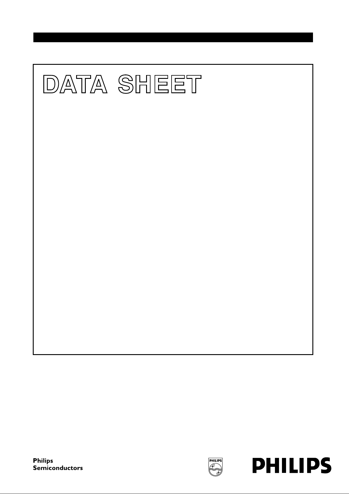
4 BLOCK DIAGRAMS
dbook, full pagewidth
EXPANSION PORT INTERFACE
DATA
FORMATTER/
REFORMATTER
AND
REFERENCE
SIGNAL
GENERATION
ACQUISITION
CONTROL
BCS
CONTROL
CSM
DITHERING
γ-CORRECTION
OUTPUT FORMATTER
OUTPUT FIFO REGISTER
HORIZONTAL
PRESCALING
HORIZONTAL
FINE
SCALING
Y
UV
H
PXQ
V
Y
UV
Y
U
V
VERTICAL PROCESSING
SCALING UNIT
CONTROL
I
2
C
CONTROL
controls
status
VRO31 to 0
57 to 65, 70 to 81, 86 to 96
47
HGTV
VSYV
FLDV
46
454855
54
PXQV
INCADR
HFL
VCLKVOEN
V
DDD(core) 1 to 4
V
SSD(core) 1 to 4
V
DDD(bord) 1 to 12
V
SSD(bord) 1 to 11
LLCIN PXQIN HIN VIN
VIDH7 to 0 VIDL7 to 0 LLCIO PXQIO HIO VIO FDIO
reference
YIN7 to 0
UVIN7 to 0
CREF
HREF
VS
LLC
CLK
SCL
PORT3 to 0
SDA
IICSA
RES
YUV
RGB
1 125 126 127 105 to 112 117 to 124 128 104 103 102 97
18 to 11
28 to 21
6
7
8
32
31
33
42
5243 44 49 50 56
38 to 41
5
VMUX
AP SP BTST
Y
U
V
LINE
MEMORY
ARITHMETIC
EXPANSION PORT
SAA7140A
VRAM
PORT
DMSD
PORT
MHA117
Fig.1 Block diagram (SAA7140A).
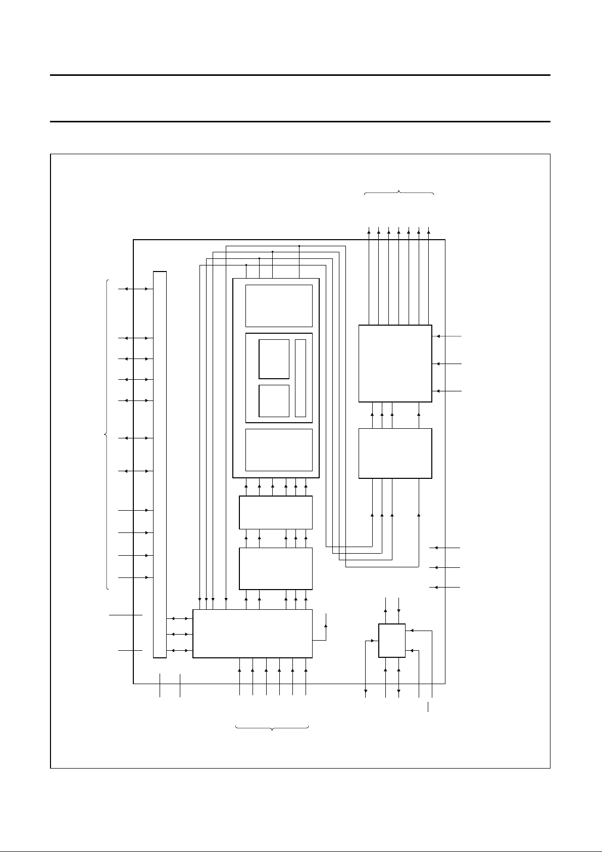
1996 Sep 04 5
Philips Semiconductors Objective specification
High Performance Scaler (HPS) SAA7140A; SAA7140B
andbook, full pagewidth
EXPANSION PORT INTERFACE
DATA
FORMATTER/
REFORMATTER
AND
REFERENCE
SIGNAL
GENERATION
ACQUISITION
CONTROL
BCS
CONTROL
CSM
DITHERING
γ-CORRECTION
OUTPUT FORMATTER
OUTPUT FIFO REGISTER
HORIZONTAL
PRESCALING
HORIZONTAL
FINE
SCALING
Y
UV
H
PXQ
V
Y
UV
Y
U
V
VERTICAL PROCESSING
SCALING UNIT
CONTROL
I
2
C
CONTROL
controls
status
VRO31 to 0
57 to 65, 70 to 81, 86 to 96
47
HGTV
VSYV
FLDV
46
454855
54
PXQV
INCADR
HFL
VCLKVOEN
V
DDD1 to 16
V
SSD1 to 15
LLCIN PXQIN HIN VIN
VIDH7 to 0 VIDL7 to 0 LLCIO PXQIO HIO VIO FDIO
reference
YIN7 to 0
UVIN7 to 0
CREF
HREF
VS
LLC
CLK
SCL
PORT3 to 0
SDA
IICSA
RES
YUV
RGB
1 125 126 127 105 to 112 117 to 124 128 104 103 102 97
18 to 11
28 to 21
6
7
8
32
31
33
42
5243 44 49 50 56
38 to 41
5
VMUX
AP SP BTST
Y
U
V
LINE
MEMORY
ARITHMETIC
EXPANSION PORT
SAA7140B
VRAM
PORT
DMSD
PORT
MHA360
Fig.2 Block diagram (SAA7140B).

1996 Sep 04 6
Philips Semiconductors Objective specification
High Performance Scaler (HPS) SAA7140A; SAA7140B
5 PINNING (SAA7140A)
SYMBOL PIN I/O DESCRIPTION
LLCIN 1 I line-locked system clock input; expansion port
V
DDD(bord)1
2 − digital border supply voltage 1 (+5 V)
V
SSD(bord)1
3 − digital border ground 1 (0 V)
V
DDD(bord)2
4 − digital border supply voltage 2 (+5 V)
LLC 5 I line-locked system clock input, maximum 32 MHz (2 × pixel rate); DMSD port
CREF 6 I clock qualifier input (HIGH indicates valid input data YUV on DMSD port)
HREF 7 I horizontal reference input signal; DMSD port
VS 8 I vertical sync input signal; DMSD port
V
DDD(core)1
9 − digital core supply voltage 1 (+3.3 V)
V
SSD(bord)2
10 − digital border ground 2 (0 V)
YIN0 11 I luminance input data (bit 0); DMSD port
YIN1 12 I luminance input data (bit 1); DMSD port
YIN2 13 I luminance input data (bit 2); DMSD port
YIN3 14 I luminance input data (bit 3); DMSD port
YIN4 15 I luminance input data (bit 4); DMSD port
YIN5 16 I luminance input data (bit 5); DMSD port
YIN6 17 I luminance input data (bit 6); DMSD port
YIN7 18 I luminance input data (bit 7); DMSD port
V
DDD(bord)3
19 − digital border supply voltage 3 (+5 V)
V
SSD(core)1
20 − digital core ground 1 (0 V)
UVIN0 21 I time-multiplexed colour-difference input data (bit 0); DMSD port
UVIN1 22 I time-multiplexed colour-difference input data (bit 1); DMSD port
UVIN2 23 I time-multiplexed colour-difference input data (bit 2); DMSD port
UVIN3 24 I time-multiplexed colour-difference input data (bit 3); DMSD port
UVIN4 25 I time-multiplexed colour-difference input data (bit 4); DMSD port
UVIN5 26 I time-multiplexed colour-difference input data (bit 5); DMSD port
UVIN6 27 I time-multiplexed colour-difference input data (bit 6); DMSD port
UVIN7 28 I time-multiplexed colour-difference input data (bit 7); DMSD port
V
DDD(bord)4
29 − digital border supply voltage 4 (+5 V)
V
SSD(bord)3
30 − digital border ground 3 (0 V)
SDA 31 I/O serial data input/output (I
2
C-bus)
SCL 32 I serial clock input (I
2
C-bus)
IICSA 33 I set address input (I
2
C-bus)
V
DDD(bord)5
34 − digital border supply voltage 5 (+5 V)
V
SSD(bord)4
35 − digital border ground 4 (0 V)
V
DDD(bord)6
36 − digital border supply voltage 6 (+5 V)
V
SSD(bord)5
37 − digital border ground 5 (0 V)
PORT3 38 I/O general purpose port 3 input/output (set via I
2
C-bus)
PORT2 39 I/O general purpose port 2 input/output (set via I
2
C-bus)
PORT1 40 I/O general purpose port 1 input/output (set via I
2
C-bus)

1996 Sep 04 7
Philips Semiconductors Objective specification
High Performance Scaler (HPS) SAA7140A; SAA7140B
PORT0 41 I/O general purpose port 0 input/output (set via I2C-bus)
RES 42 I reset input (active LOW for at least 30 clock cycles)
AP 43 I connected to ground (action pin for testing)
SP 44 I connected to ground (shift pin for testing)
FLDV 45 O field identification output signal; VRAM port
VSYV 46 O vertical sync output signal; VRAM port
HGTV 47 O horizontal reference output signal; VRAM port
PXQV 48 O pixel qualifier output signal to mark active pixels of a qualified line; VRAM port
BTST 49 I connected to ground; BTST = HIGH sets all outputs to high-impedance state
(testing)
VOEN 50 I enable input signal for VRAM port
V
DDD(core)2
51 − digital core supply voltage 2 (+3.3 V)
VMUX 52 I VRAM output multiplexing, control input for the 32 to 16-bit multiplexer
V
SSD(core)2
53 − digital core ground 2 (0 V)
HFL 54 O FIFO half-full flag output signal
INCADR 55 O line increment/vertical reset control output
VCLK 56 I/O clock input/output signal for VRAM port
VRO31 57 O 32-bit digital VRAM port output (bit 31)
VRO30 58 O 32-bit digital VRAM port output (bit 30)
VRO29 59 O 32-bit digital VRAM port output (bit 29)
VRO28 60 O 32-bit digital VRAM port output (bit 28)
VRO27 61 O 32-bit digital VRAM port output (bit 27)
VRO26 62 O 32-bit digital VRAM port output (bit 26)
VRO25 63 O 32-bit digital VRAM port output (bit 25)
VRO24 64 O 32-bit digital VRAM port output (bit 24)
VRO23 65 O 32-bit digital VRAM port output (bit 23)
V
DDD(bord)7
66 − digital border supply voltage 7 (+5 V)
V
SSD(bord)6
67 − digital border ground 6 (0 V)
V
DDD(bord)8
68 − digital border supply voltage 8 (+5 V)
V
SSD(bord)7
69 − digital border ground 7 (0 V)
VRO22 70 O 32-bit VRAM port output (bit 22)
VRO21 71 O 32-bit VRAM port output (bit 21)
VRO20 72 O 32-bit VRAM port output (bit 20)
VRO19 73 O 32-bit VRAM port output (bit 19)
VRO18 74 O 32-bit VRAM port output (bit 18)
VRO17 75 O 32-bit VRAM port output (bit 17)
VRO16 76 O 32-bit VRAM port output (bit 16)
VRO15 77 O 32-bit VRAM port output (bit 15)
VRO14 78 O 32-bit VRAM port output (bit 14)
VRO13 79 O 32-bit VRAM port output (bit 13)
VRO12 80 O 32-bit VRAM port output (bit 12)
SYMBOL PIN I/O DESCRIPTION
1996 Sep 04 8
Philips Semiconductors Objective specification
High Performance Scaler (HPS) SAA7140A; SAA7140B
VRO11 81 O 32-bit VRAM port output (bit 11)
V
SSD(bord)8
82 − digital border ground 8 (0 V)
V
DDD(bord)9
83 − digital border supply voltage 9 (+5 V)
V
SSD(core)3
84 − digital core ground 3 (0 V)
V
DDD(core)3
85 − digital core supply voltage 3 (+3.3 V)
VRO10 86 O 32-bit VRAM port output (bit 10)
VRO9 87 O 32-bit VRAM port output (bit 9)
VRO8 88 O 32-bit VRAM port output (bit 8)
VRO7 89 O 32-bit VRAM port output (bit 7)
VRO6 90 O 32-bit VRAM port output (bit 6)
VRO5 91 O 32-bit VRAM port output (bit 5)
VRO4 92 O 32-bit VRAM port output (bit 4)
VRO3 93 O 32-bit VRAM port output (bit 3)
VRO2 94 O 32-bit VRAM port output (bit 2)
VRO1 95 O 32-bit VRAM port output (bit 1)
VRO0 96 O 32-bit VRAM port output (bit 0)
FDIO 97 I/O field identification output signal; 7196 DIR input signal expansion port, I
2
C-bus
controlled
V
DDD(bord)10
98 − digital border supply voltage 10 (+5 V)
V
SSD(bord)9
99 − digital border ground 9 (0 V)
V
DDD(bord)11
100 − digital border supply voltage 11 (+5 V)
V
SSD(bord)10
101 − digital border ground 10 (0 V)
VIO 102 I/O vertical sync input/output signal; expansion port
HIO 103 I/O horizontal sync input/output signal; expansion port
PXQIO 104 I/O pixel qualifier input/output signal to mark valid pixels; expansion port
VIDH7 105 I/O bidirectional expansion port, high byte (bit 7) in 16-bit mode luminance
component Y
VIDH6 106 I/O bidirectional expansion port, high byte (bit 6) in 16-bit mode luminance
component Y
VIDH5 107 I/O bidirectional expansion port, high byte (bit 5) in 16-bit mode luminance
component Y
VIDH4 108 I/O bidirectional expansion port, high byte (bit 4) in 16-bit mode luminance
component Y
VIDH3 109 I/O bidirectional expansion port, high byte (bit 3) in 16-bit mode luminance
component Y
VIDH2 110 I/O bidirectional expansion port, high byte (bit 2) in 16-bit mode luminance
component Y
VIDH1 111 I/O bidirectional expansion port, high byte (bit 1) in 16-bit mode luminance
component Y
VIDH0 112 I/O bidirectional expansion port, high byte (bit 0) in 16-bit mode luminance
component Y
V
DDD(bord)12
113 − digital border supply voltage 12 (+5 V)
SYMBOL PIN I/O DESCRIPTION
1996 Sep 04 9
Philips Semiconductors Objective specification
High Performance Scaler (HPS) SAA7140A; SAA7140B
V
SSD(bord)11
114 − digital border ground 11 (0 V)
V
DDD(core)4
115 − digital core supply voltage 4 (+3.3 V)
V
SSD(core)4
116 − digital core ground 4 (0 V)
VIDL7 117 I/O bidirectional expansion port, low byte (bit 7) in 16-bit mode time-multiplexed
colour-difference components U and V
VIDL6 118 I/O bidirectional expansion port, low byte (bit 6) in 16-bit mode time-multiplexed
colour-difference components U and V
VIDL5 119 I/O bidirectional expansion port, low byte (bit 5) in 16-bit mode time-multiplexed
colour-difference components U and V
VIDL4 120 I/O bidirectional expansion port, low byte (bit 4) in 16-bit mode time-multiplexed
colour-difference components U and V
VIDL3 121 I/O bidirectional expansion port, low byte (bit 3) in 16-bit mode time-multiplexed
colour-difference components U and V
VIDL2 122 I/O bidirectional expansion port, low byte (bit 2) in 16-bit mode time-multiplexed
colour-difference components U and V
VIDL1 123 I/O bidirectional expansion port, low byte (bit 1) in 16-bit mode time-multiplexed
colour-difference components U and V
VIDL0 124 I/O bidirectional expansion port, low byte (bit 0) in 16-bit mode time-multiplexed
colour-difference components U and V
PXQIN 125 I pixel qualifier input signal to mark valid pixels; expansion port
HIN 126 I horizontal sync input signal; expansion port
VIN 127 I vertical sync input signal; expansion port
LLCIO 128 I/O line-locked system clock input/output; expansion port
SYMBOL PIN I/O DESCRIPTION
1996 Sep 04 10
Philips Semiconductors Objective specification
High Performance Scaler (HPS) SAA7140A; SAA7140B
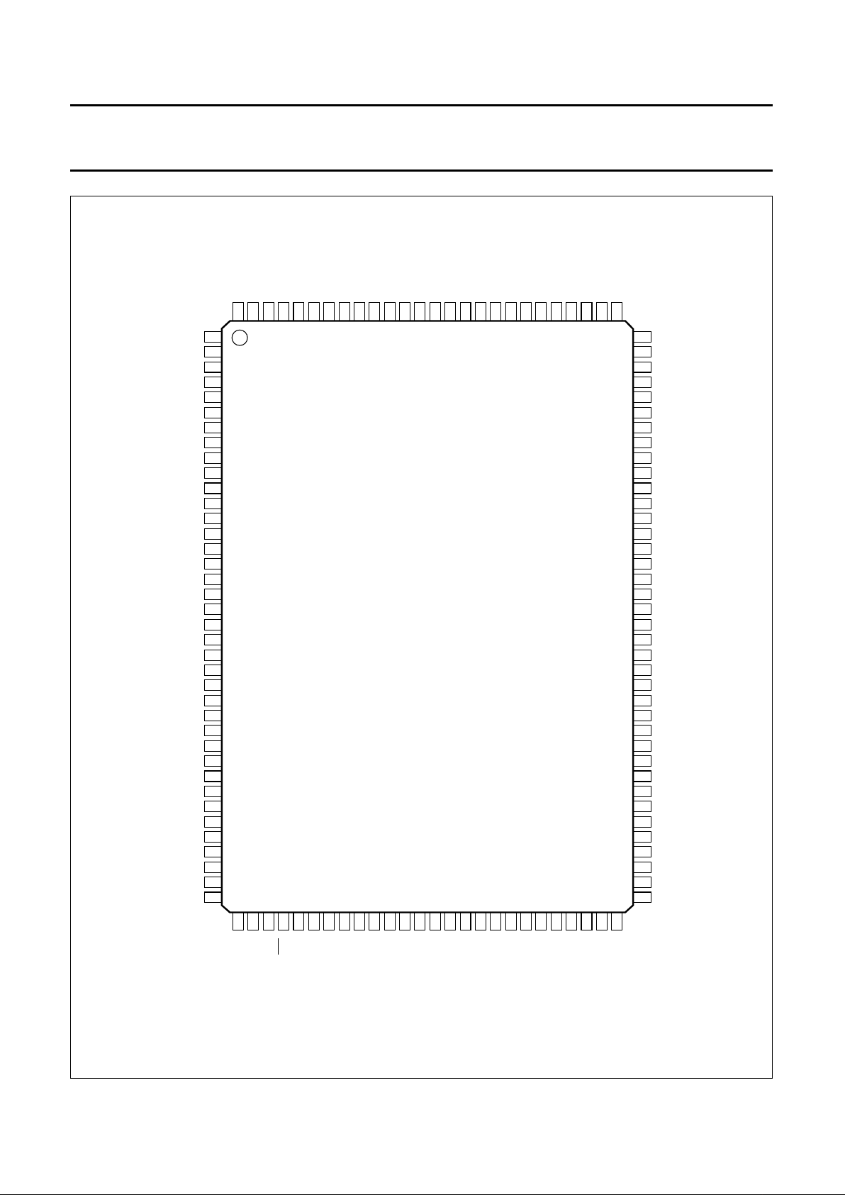
Fig.3 Pin configuration (SAA7140A).
handbook, full pagewidth
MHA362
SAA7140A
2
1
3
4
5
6
7
8
9
10
11
12
13
14
15
16
17
18
19
20
21
22
23
24
25
26
27
28
29
30
31
32
33
34
35
36
37
38
101
102
100
99
98
97
96
95
94
93
92
91
90
89
88
87
86
85
84
83
82
81
80
79
78
77
76
75
74
73
72
71
70
69
68
67
66
65
V
SSD(bord)10
VIO
V
DDD(bord)11
V
SSD(bord)9
V
DDD(bord)10
FDIO
VRO0
VRO1
VRO2
VRO3
VRO4
VRO5
VRO5
VRO7
VRO8
VRO9
VRO10
V
DDD(core)3
V
SSD(core)3
V
DDD(bord)9
V
SSD(bord)8
VRO11
VRO12
VRO13
VRO14
VRO15
VRO16
VRO17
VRO18
VRO19
VRO20
VRO21
VRO22
V
SSD(bord)7
V
DDD(bord)8
V
SSD(bord)6
V
DDD(bord)7
VRO23
V
DDD(bord)1
LLCIN
V
SSD(bord)1
V
DDD(bord)2
LCC
CREF
HREF
VS
V
DDD(core)1
V
SSD(bord)2
YIN0
YIN1
YIN2
YIN3
YIN4
YIN5
YIN6
YIN7
V
DDD(bord)3
V
SSD(core)1
UVIN0
UVIN1
UVIN2
UVIN3
UVIN4
UVIN5
UVIN6
UVIN7
V
DDD(bord)4
V
SSD(bord)3
SDA
SCL
IICSA
V
DDD(bord)5
V
SSD(bord)4
V
DDD(bord)6
V
SSD(bord)5
PORT3
40394142434445464748495051525354555657585960616263
64
127
128
126
125
124
123
122
121
120
119
118
117
116
115
114
113
112
111
110
109
108
107
106
105
104
103
VIN
LLCIO
HIN
PXQIN
VIDL0
VIDL1
VIDL2
VIDL3
VIDL4
VIDL5
VIDL6
VIDL7
V
SSD(core)4
V
DDD(core)4
V
SSD(bord)11
V
DDD(bord)12
VIDH0
VIDH1
VIDH2
VIDH3
VIDH4
VIDH5
VIDH6
VIDH7
PXQIO
HIO
PORT1
PORT2
PORT0
RES
AP
SP
FLDV
VSYV
HGTV
PXQV
BTST
VOEN
V
DDD(core)2
VMUX
V
SSD(core)2
HFL
INCADR
VCLK
VRO31
VRO30
VRO29
VRO28
VRO27
VRO26
VRO25
VRO24
1996 Sep 04 11
Philips Semiconductors Objective specification
High Performance Scaler (HPS) SAA7140A; SAA7140B
6 PINNING (SAA7140B)
SYMBOL PIN I/O DESCRIPTION
LLCIN 1 I line-locked system clock input; expansion port
V
DDD1
2 − digital supply voltage 1 (+3.3 V)
V
SSD1
3 − digital ground 1 (0 V)
V
DDD2
4 − digital supply voltage 2 (+3.3 V)
LLC 5 I line-locked system clock input, maximum 32 MHz (2 × pixel rate); DMSD port
CREF 6 I clock qualifier input (HIGH indicates valid input data YUV on DMSD port)
HREF 7 I horizontal reference input signal; DMSD port
VS 8 I vertical sync input signal; DMSD port
V
DDD3
9 − digital supply voltage 3 (+3.3 V)
V
SSD2
10 − digital ground 2 (0 V)
YIN0 11 I luminance input data (bit 0); DMSD port
YIN1 12 I luminance input data (bit 1); DMSD port
YIN2 13 I luminance input data (bit 2); DMSD port
YIN3 14 I luminance input data (bit 3); DMSD port
YIN4 15 I luminance input data (bit 4); DMSD port
YIN5 16 I luminance input data (bit 5); DMSD port
YIN6 17 I luminance input data (bit 6); DMSD port
YIN7 18 I luminance input data (bit 7); DMSD port
V
DDD4
19 − digital supply voltage 4 (+3.3 V)
V
SSD3
20 − digital ground 3 (0 V)
UVIN0 21 I time-multiplexed colour-difference input data (bit 0); DMSD port
UVIN1 22 I time-multiplexed colour-difference input data (bit 1); DMSD port
UVIN2 23 I time-multiplexed colour-difference input data (bit 2); DMSD port
UVIN3 24 I time-multiplexed colour-difference input data (bit 3); DMSD port
UVIN4 25 I time-multiplexed colour-difference input data (bit 4); DMSD port
UVIN5 26 I time-multiplexed colour-difference input data (bit 5); DMSD port
UVIN6 27 I time-multiplexed colour-difference input data (bit 6); DMSD port
UVIN7 28 I time-multiplexed colour-difference input data (bit 7); DMSD port
V
DDD5
29 − digital supply voltage 5 (+3.3 V)
V
SSD4
30 − digital ground 4 (0 V)
SDA 31 I/O serial data input/output (I
2
C-bus)
SCL 32 I serial clock input (I
2
C-bus)
IICSA 33 I set address input (I
2
C-bus)
V
DDD6
34 − digital supply voltage 6 (+3.3 V)
V
SSD5
35 − digital ground 5 (0 V)
V
DDD7
36 − digital supply voltage 7 (+3.3 V)
V
SSD6
37 − digital ground 6 (0 V)
PORT3 38 I/O general purpose port 3 input/output (set via I
2
C-bus)
PORT2 39 I/O general purpose port 2 input/output (set via I
2
C-bus)
PORT1 40 I/O general purpose port 1 input/output (set via I
2
C-bus)
1996 Sep 04 12
Philips Semiconductors Objective specification
High Performance Scaler (HPS) SAA7140A; SAA7140B
PORT0 41 I/O general purpose port 0 input/output (set via I2C-bus)
RES 42 I reset input (active LOW for at least 30 clock cycles)
AP 43 I connected to ground (action pin for testing)
SP 44 I connected to ground (shift pin for testing)
FLDV 45 O field identification output signal; VRAM port
VSYV 46 O vertical sync output signal; VRAM port
HGTV 47 O horizontal reference output signal; VRAM port
PXQV 48 O pixel qualifier output signal to mark active pixels of a qualified line; VRAM port
BTST 49 I connected to ground; BTST = HIGH sets all outputs to high-impedance state
(testing)
VOEN 50 I enable input signal for VRAM port
V
DDD8
51 − digital supply voltage 8 (+3.3 V)
VMUX 52 I VRAM output multiplexing, control input for the 32 to 16-bit multiplexer
V
SSD7
53 − digital ground 7 (0 V)
HFL 54 O FIFO half-full flag output signal
INCADR 55 O line increment/vertical reset control output
VCLK 56 I/O clock input/output signal for VRAM port
VRO31 57 O 32-bit digital VRAM port output (bit 31)
VRO30 58 O 32-bit digital VRAM port output (bit 30)
VRO29 59 O 32-bit digital VRAM port output (bit 29)
VRO28 60 O 32-bit digital VRAM port output (bit 28)
VRO27 61 O 32-bit digital VRAM port output (bit 27)
VRO26 62 O 32-bit digital VRAM port output (bit 26)
VRO25 63 O 32-bit digital VRAM port output (bit 25)
VRO24 64 O 32-bit digital VRAM port output (bit 24)
VRO23 65 O 32-bit digital VRAM port output (bit 23)
V
DDD9
66 − digital supply voltage 9 (+3.3 V)
V
SSD8
67 − digital ground 8 (0 V)
V
DDD10
68 − digital supply voltage 10 (+3.3 V)
V
SSD9
69 − digital ground 9 (0 V)
VRO22 70 O 32-bit VRAM port output (bit 22)
VRO21 71 O 32-bit VRAM port output (bit 21)
VRO20 72 O 32-bit VRAM port output (bit 20)
VRO19 73 O 32-bit VRAM port output (bit 19)
VRO18 74 O 32-bit VRAM port output (bit 18)
VRO17 75 O 32-bit VRAM port output (bit 17)
VRO16 76 O 32-bit VRAM port output (bit 16)
VRO15 77 O 32-bit VRAM port output (bit 15)
VRO14 78 O 32-bit VRAM port output (bit 14)
VRO13 79 O 32-bit VRAM port output (bit 13)
VRO12 80 O 32-bit VRAM port output (bit 12)
SYMBOL PIN I/O DESCRIPTION

1996 Sep 04 13
Philips Semiconductors Objective specification
High Performance Scaler (HPS) SAA7140A; SAA7140B
VRO11 81 O 32-bit VRAM port output (bit 11)
V
SSD10
82 − digital ground 10 (0 V)
V
DDD11
83 − digital supply voltage 11 (+3.3 V)
V
SSD11
84 − digital ground 11 (0 V)
V
DDD12
85 − digital supply voltage 12 (+3.3 V)
VRO10 86 O 32-bit VRAM port output (bit 10)
VRO9 87 O 32-bit VRAM port output (bit 9)
VRO8 88 O 32-bit VRAM port output (bit 8)
VRO7 89 O 32-bit VRAM port output (bit 7)
VRO6 90 O 32-bit VRAM port output (bit 6)
VRO5 91 O 32-bit VRAM port output (bit 5)
VRO4 92 O 32-bit VRAM port output (bit 4)
VRO3 93 O 32-bit VRAM port output (bit 3)
VRO2 94 O 32-bit VRAM port output (bit 2)
VRO1 95 O 32-bit VRAM port output (bit 1)
VRO0 96 O 32-bit VRAM port output (bit 0)
FDIO 97 I/O field identification output signal; 7196 DIR input signal expansion port, I
2
C-bus
controlled
V
DDD13
98 − digital supply voltage 13 (+3.3 V)
V
SSD12
99 − digital ground 12 (0 V)
V
DDD14
100 − digital supply voltage 14 (+3.3 V)
V
SSD13
101 − digital ground 13 (0 V)
VIO 102 I/O vertical sync input/output signal; expansion port
HIO 103 I/O horizontal sync input/output signal; expansion port
PXQIO 104 I/O pixel qualifier input/output signal to mark valid pixels; expansion port
VIDH7 105 I/O bidirectional expansion port, high byte (bit 7) in 16-bit mode luminance
component Y
VIDH6 106 I/O bidirectional expansion port, high byte (bit 6) in 16-bit mode luminance
component Y
VIDH5 107 I/O bidirectional expansion port, high byte (bit 5) in 16-bit mode luminance
component Y
VIDH4 108 I/O bidirectional expansion port, high byte (bit 4) in 16-bit mode luminance
component Y
VIDH3 109 I/O bidirectional expansion port, high byte (bit 3) in 16-bit mode luminance
component Y
VIDH2 110 I/O bidirectional expansion port, high byte (bit 2) in 16-bit mode luminance
component Y
VIDH1 111 I/O bidirectional expansion port, high byte (bit 1) in 16-bit mode luminance
component Y
VIDH0 112 I/O bidirectional expansion port, high byte (bit 0) in 16-bit mode luminance
component Y
V
DDD15
113 − digital supply voltage 15 (+3.3 V)
SYMBOL PIN I/O DESCRIPTION

1996 Sep 04 14
Philips Semiconductors Objective specification
High Performance Scaler (HPS) SAA7140A; SAA7140B
V
SSD14
114 − digital ground 14 (0 V)
V
DDD16
115 − digital supply voltage 16 (+3.3 V)
V
SSD15
116 − digital ground 15 (0 V)
VIDL7 117 I/O bidirectional expansion port, low byte (bit 7) in 16-bit mode time-multiplexed
colour-difference components U and V
VIDL6 118 I/O bidirectional expansion port, low byte (bit 6) in 16-bit mode time-multiplexed
colour-difference components U and V
VIDL5 119 I/O bidirectional expansion port, low byte (bit 5) in 16-bit mode time-multiplexed
colour-difference components U and V
VIDL4 120 I/O bidirectional expansion port, low byte (bit 4) in 16-bit mode time-multiplexed
colour-difference components U and V
VIDL3 121 I/O bidirectional expansion port, low byte (bit 3) in 16-bit mode time-multiplexed
colour-difference components U and V
VIDL2 122 I/O bidirectional expansion port, low byte (bit 2) in 16-bit mode time-multiplexed
colour-difference components U and V
VIDL1 123 I/O bidirectional expansion port, low byte (bit 1) in 16-bit mode time-multiplexed
colour-difference components U and V
VIDL0 124 I/O bidirectional expansion port, low byte (bit 0) in 16-bit mode time-multiplexed
colour-difference components U and V
PXQIN 125 I pixel qualifier input signal to mark valid pixels; expansion port
HIN 126 I horizontal sync input signal; expansion port
VIN 127 I vertical sync input signal; expansion port
LLCIO 128 I/O line-locked system clock input/output; expansion port
SYMBOL PIN I/O DESCRIPTION
1996 Sep 04 15
Philips Semiconductors Objective specification
High Performance Scaler (HPS) SAA7140A; SAA7140B
Fig.4 Pin configuration (SAA7140B).
handbook, full pagewidth
MHA359
SAA7140B
2
1
3
4
5
6
7
8
9
10
11
12
13
14
15
16
17
18
19
20
21
22
23
24
25
26
27
28
29
30
31
32
33
34
35
36
37
38
101
102
100
99
98
97
96
95
94
93
92
91
90
89
88
87
86
85
84
83
82
81
80
79
78
77
76
75
74
73
72
71
70
69
68
67
66
65
V
SSD13
VIO
V
DDD14
V
SSD12
V
DDD13
FDIO
VRO0
VRO1
VRO2
VRO3
VRO4
VRO5
VRO6
VRO7
VRO8
VRO9
VRO10
V
DDD12
V
SSD11
V
DDD11
V
SSD10
VRO11
VRO12
VRO13
VRO14
VRO15
VRO16
VRO17
VRO18
VRO19
VRO20
VRO21
VRO22
V
SSD9
V
DDD10
V
SSD8
V
DDD9
VRO23
V
DDD1
LLCIN
V
SSD1
V
DDD2
LLC
CREF
HREF
VS
V
DDD3
V
SSD2
YIN0
YIN1
YIN2
YIN3
YIN4
YIN5
YIN6
YIN7
V
DDD4
V
SSD3
UVIN0
UVIN1
UVIN2
UVIN3
UVIN4
UVIN5
UVIN6
UVIN7
V
DDD5
V
SSD4
SDA
SCL
IICSA
V
DDD6
V
SSD5
V
DDD7
V
SSD6
PORT3
40394142434445464748495051525354555657585960616263
64
127
128
126
125
124
123
122
121
120
119
118
117
116
115
114
113
112
111
110
109
108
107
106
105
104
103
VIN
LLCIO
HIN
PXQIN
VIDL0
VIDL1
VIDL2
VIDL3
VIDL4
VIDL5
VIDL6
VIDL7
V
SSD15VDDD16VSSD14VDDD15
VIDH0
VIDH1
VIDH2
VIDH3
VIDH4
VIDH5
VIDH6
VIDH7
PXQIO
HIO
PORT1
PORT2
PORT0
AP
SP
FLDV
VSYV
HGTV
PXQV
BTST
VOEN
V
DDD8
VMUX
V
SSD7
HFL
INCADR
VCLK
VRO31
VRO30
VRO29
VRO28
VRO27
VRO26
VRO25
VRO24
RES

1996 Sep 04 16
Philips Semiconductors Objective specification
High Performance Scaler (HPS) SAA7140A; SAA7140B
7 FUNCTIONAL DESCRIPTION
The SAA7140A and SAA7140B accepts YUV data in a
16-bit wide parallel format at the DMSD port and accepts
YUV input in a 16-bit wide parallel format and in an 8-bit
byte-multiplexed Cb-Y-Cr-Y- format (CCIR-656 or
D1 oriented) at the expansion port.
Depending on the selected port modes, the incoming data
is formatted to the internal data representation, where
reference signals or codes are detected in the Data
Formatter/Reformatter (DFR). The horizontal and vertical
timing reference can be defined under I
2
C-bus control.
Based on that timing reference, the active processing
window is defined in a versatile way via the programming.
Two programming sets can be loaded simultaneously, and
become valid for processing in a field alternating way.
Before being processed in the central scaling unit, the
incoming data passes through the BCS control unit where
monitor control functions, for adjusting brightness, contrast
(luminance) and saturation (chrominance) are
implemented.
The scaling is performed in three steps:
1. Horizontal prescaling (bandwidth limitation for
anti-aliasing, via FIR prefiltering and subsampling)
2. Vertical scaling (generating phase interpolated or
vertically low-passed lines)
3. Horizontal variable phase scaling (phase-correct
scaling to the new geometric relationships).
The scaled output data is fed back to the DFR unit and
may be used as output signals from the bidirectional
expansion port (if the mode is selected). They are
converted in parallel from the YUV to the RGB domain in a
digital matrix. Anti-gamma correction of gamma-corrected
input signals can be performed in the RGB data path.
The output formatter then formats the scaled data to one
of the various output formats (e.g. monochrome, 16-bit
YUV or 32-bit RGB (5, 5, 5).
To ease frame buffer applications, the data can be
transferred in a synchronous way (transparent mode),
using separate reference and qualifier signals and a
continuous output clock (VCLK). The data can also be
transferred in an asynchronous way (burst mode) using
the HFL and INCADR flags and a discontinuous input
clock burst on VCLK.
In a typical application, the 16-bit wide YUV input receives
clock, sync and data from a video decoder (SAA71xx) via
the DMSD port. An MPEG compression/decompression
circuit can be connected at the expansion port to receive
the decoder data, scaled or unscaled, or to deliver data to
the scaling processor. The scaling operation of the
SAA7140A and SAA7140B can be performed on the data
from a video decoder, or on the data from the
MPEG-codec at the expansion port input. The source
selection can be static or toggled on a field-by-field basis.
For example, during the odd field the video decoder signal
is scaled in accordance with the ‘odd’ parameter set for
display in a window. The compression codec receives
unscaled data. During the even field the decompressed
data from the MPEG decoder gets sized for a second
display window in accordance with the ‘even’ parameter
set. The resulting output from the scaling operation is
delivered via the 32-bit wide output (VRAM port) and to the
expansion port output (optional).
7.1 Data format/reformatter and reference signal
generation
The video data can be formatted/reformatted in
accordance with the selected expansion port mode, from
16-bit (DMSD port) to serial 8-bit (expansion port output),
from serial 8-bit (expansion port input) to internal parallel
16-bit format and from 24-bit (scaler output) to 16-bit/8-bit
respectively (expansion port output). The definition of the
timing references for the acquisition and field detection
(polarity and edge selection) are based on the selected
reference signal source. The field detector regenerates the
field information from the selected incoming reference
signals (see Fig.5).
The field sequence flag (FLD), detects the state of the
H-sync signal at the reference edge of the V-sync signal.
The detection is controlled by I
2
C-bus bits REVFLD and
INVOE. The detection output can be seen on pins FLDV
and FDIO (if FLDC = 0). Bits IREGS and SREGS control
the mapping of the detected sequence to the I2C-bus
register sets A and B (I2C-bus subaddress 02 to 1F and
22 to 3F).
1996 Sep 04 17
Philips Semiconductors Objective specification
High Performance Scaler (HPS) SAA7140A; SAA7140B
Fig.5 Field detection/register set mapping.
FLD detection modes (I2C-bus bits FICO1 and FICO0);
(1) In the normal mode: the FLD signal is detected from the incoming
H andV signals.
In the improved mode: the FLD signal is resynchronized only after
the H andV sequence runs stable for a certain period of time.
In the force toggle mode: the FLD signal toggles with every event on
the V signal (His independent).
Register set mapping modes (I2C-bus bits IREGS and SREGS);
The FLD_IIC signal carries the detected FLD or the inverted FLD.
The signal is fixed to 0 (Register setA forced) or forced to 1
(Register set A forced).
handbook, full pagewidth
REGISTER 00
FIELD DETECTION
(1)
SOURCE SELECT
FIELD DETECTION
SOURCE SELECT
SCALER
REGISTER SET
MAPPING FIELD
REGISTER 00
H/V DMSD
H/V expansion port
V source select
n × τ
m × τ
FIDO
(expansion port)
FLDV
(VRAM)
active
vertical
edge
active
horizontal
edge
H/V
source
select
MULTIPLEXER
AQUISITION CONTROL
REGISTER A REGISTER B
select
SCALER
HV
(or frame sync)
FLD IIC
H
F
V
F
(corresponding
to VF)
active
horizontal
state
active
vertical
edge
detected field
MHA118
INVOE
REVFLD
7.1.1 DATA FORMATS AND REFERENCE SIGNALS OF THE
DMSD PORT
The 16-bit YUV colour difference and luminance signals
(straight binary) are available in parallel on a 16-bit wide
data stream. The code is in accordance with CCIR-601;
black = 16, white = 235, no colour = 128, 100% colour
saturation = 16 to 240 etc. Overshoots and undershoots
are permitted and supported, i.e. processed as they are.
The 16-bit wide YUV data format from the DMSD port
(input only) is defined with Line-Locked Clock (LLC) with a
double pixel clock frequency. Every second clock cycle is
qualified with CREF, in pixel rate frequency.
The internal processing of the SAA7140A and SAA7140B
relies on the presence of LLC, i.e. a clock of at least twice
the sampling rate of the input data stream. The maximum
LLC rate is 32 MHz.
The horizontal sync input (HREF) may be supplied as a
H-pulse or horizontal gate signal. The positive or negative
edge, (programmable by I
2
C-bus bit REHAW), indicates
the horizontal timing reference. The first valid pixels may
occur not exactly at the start of the line but with a certain
offset (counted in qualified pixels).

1996 Sep 04 18
Philips Semiconductors Objective specification
High Performance Scaler (HPS) SAA7140A; SAA7140B
The vertical timing is indicated by the positive or negative
edge (programmable by I2C-bus bit REVAW) of the sync
input signal VS. The first valid line may occur not exactly
at the start of the field but with a certain offset, counted in
lines, with qualified pixels. Input signal VS defines, in
relation to HREF, the odd/even field detection
(see
SAA7191B
).
7.1.2 D
ATA FORMATS AND REFERENCE SIGNALS OF THE
EXPANSION PORT
The expansion port (input/output) supports several modes;
simultaneous (parallel) D1 input and D1 output (full
duplex) with auxiliary sync and qualifying signals, or 16-bit
wide YUV input or output (half duplex), selected via
programming with clock, qualify and sync signal.
A discontinuous data stream is supported by accepting or
generating a pixel/byte qualifying signal (PXQ), a
generalization of the CREF definition at the DMSD port
(PXQ = 1 qualified pixel, PXQ = 0 invalid data).
16-bit YUV (half duplex mode = field alternating data I/O):
16-bit YUV data stream (Y = VIDH7 to VIDH0,
UV = VIDL7 to VIDL0). For the 16-bit YUV data input
format, PXQ is inhibited from qualifying adjacent LLC clock
cycles. There must be at least one empty clock cycle
between two valid pixels.
8-bit Cb-Y-Cr-Y; CCIR 656 or D1 (full duplex mode): the
colour difference signals and the luminance signal
(straight binary) are byte-wise multiplexed onto the same
8-bit wide data stream, with sequence and timing in
accordance with CCIR 656 recommendations (according
to D1 for 60 Hz application respectively). The code is in
accordance with CCIR 601 (black = 16, white = 235, no
colour = 128, 100% colour saturation = 16 or 240, etc.
Overshoots and undershoots are permitted and
supported, i.e. processed as they are.
If the CCIR 656 output is selected, the video signal is
clipped to 01H and FEH in order to leave the codes 00H
and FFH for SAV and EAV encoding (SAV and EAV
encoding not yet supported). The clock rate for this format
is twice the pixel clock.
The horizontal sync input HIN is processed in an identical
manner to HREF at the DMSD port. If the CCIR 656 data
input format is selected, the horizontal timing reference is
decoded from the input data stream (SAV, EAV and
SHVS = 1) or taken from the selected H-reference signal
HIN, HREF or HIO (SHVS = 0). The start condition to
enable synchronization to the correct Cb-Y-Cr-Ysequence is provided by the selected horizontal reference
signal. The sequence only increments with qualified bytes.
Instead of a vertical sync signal, as described for the
DMSD port, the expansion port also supports an odd/even
signal applied to the input pin VIN or VIO (controlled by
I
2
C-bus bit FSEL). The frame and the field timing is then
indicated by a positive or negative edge of the V input.
This may occur with a certain offset at the frame and field
start, and is normally counted in lines.
If the CCIR 656 data input format is selected, the vertical
timing reference is decoded from the input data stream by
SAV and EAV (SHVS = 1) or taken from the selected V
reference signal VIN, VS or VIO (SHVS = 0). The vertical
synchronization pin can be programmed to carry either a
vertical sync signal or an odd/even signal.
The horizontal and vertical sync outputs HIO and VIO are
expansion port mode dependent and can be selected via
the I2C-bus (VD1/VD0 and HD1/HD0):
Should the DMSD port be selected as the output source,
HIO will carry a copy of HREF and VIO will carry a copy
of VS.
If the expansion port carries data from the scaler output,
then HIO is a gate signal enveloping the range of active
video along a line and VIO is a positive sync pulse with
a length of 4 lines
If HIN/VIN is selected as the output source, HIO carries
a copy of HIN and VIO carries a copy of VIN (short cut).
If the CCIR 656 data output format is selected, the
horizontal and vertical sync output signals are only
supplied at pins HIO and VIO (SAV and EAV are not
encoded as outputs).
Due to compatibility reasons to the expansion port
definition of the SAA7194/SAA7196 circuits, the
bidirectional pins HIO, VIO and PXQIO can also be
configured as input pins (see Table 3).
The definition of the pin FDIO is I2C-bus selectable.
Configured as an output pin, FDIO carries an odd/even
signal generated in the FLD detection (see Fig.5).
Configured as an input pin, FDIO controls the direction of
the expansion port (compatibility to SAA7194/SAA7196,
(see Table 3 and Chapter 8).
1996 Sep 04 19
Philips Semiconductors Objective specification
High Performance Scaler (HPS) SAA7140A; SAA7140B
Fig.6 Timing of PXQIN for 16-bit data input from DMSD to expansion port.
handbook, full pagewidth
LLC
CREF
PXQIN
VIDL7 to 0
VIDH7 to 0
HIN
Cb0
Cr0 Cb2 Cr2
Y0 Y1 Y2 Y3
MHA126
Fig.7 Timing of PXQIO for serial 8-bit data input at expansion port.
handbook, full pagewidth
LLC
CREF
PXQIN
VIDL7 to 0
HIN
Cb Y Y Y Cr Cb
MHA130
1996 Sep 04 20
Philips Semiconductors Objective specification
High Performance Scaler (HPS) SAA7140A; SAA7140B
Fig.8 Timing of PXQIN/PXQIO for CCIR 656 data input at expansion port.
handbook, full pagewidth
LLC
CREF
PXQIN/PXQIO
PXQIN/PXQIO
VIDL7 to 0
VIDL7 to 0
FFH 00H 00H Cb SAV
Y Cr Y FFH 00H 00H
Y Cr
EAV
MHA129
Fig.9 Timing of PXQIO for non-zoomed 16-bit data output at expansion port.
handbook, full pagewidth
LLC
CREF
PXQIO
VIDL7 to 0
VIDH7 to 0
HIO
Cb0 Cr0
Cb2
Cr2
Y0 Y1
Y2
Y3
MHA127
1996 Sep 04 21
Philips Semiconductors Objective specification
High Performance Scaler (HPS) SAA7140A; SAA7140B
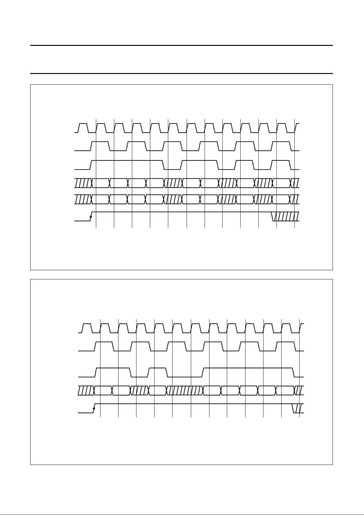
Fig.10 Timing of PXQIN for zoomed 16-bit data output at expansion port.
handbook, full pagewidth
LLC
CREF
PXQIO
VIDL7 to 0
VIDH7 to 0
HIO
Cb0 Cr0 Cb2 Cr2 Cr4 Cb4
Y0 Y1 Y2 Y3 Y5 Y6 Y4
Cb6 Cr6
Y7
MHA128
Fig.11 Timing of PXQIO for serial 8-bit data output at expansion port.
handbook, full pagewidth
LLC
CREF
PXQIO
VIDL7 to 0
Cb Y Y Y Cr Cb
Cr Y
HIO
MHA131
 Loading...