

Philips SAA7118E, SAA7118H Datasheet
INTEGRATED CIRCUITS
DATA SH EET
SAA7118
Multistandard video decoder with
adaptivecombfilterandcomponent
video input
Preliminary specification
Supersedes data of 2000 Nov 27
File under Integrated Circuits, IC22
2001 May 30

Philips Semiconductors Preliminary specification
Multistandard video decoder with adaptive
comb filter and component video input
CONTENTS
1 FEATURES
1.1 Video acquisition/clock
1.2 Video decoder
1.3 Component video processing
1.4 Video scaler
1.5 Vertical Blanking Interval (VBI) data decoder
and slicer
1.6 Audio clock generation
1.7 Digital I/O interfaces
1.8 Miscellaneous
2 APPLICATIONS
3 GENERAL DESCRIPTION
4 QUICK REFERENCE DATA
5 ORDERING INFORMATION
6 BLOCK DIAGRAM
7 PINNING
8 FUNCTIONAL DESCRIPTION
8.1 Decoder
8.2 Component video processing
8.3 Decoder output formatter
8.4 Scaler
8.5 VBI-data decoder and capture
(subaddresses 40H to 7FH)
8.6 Image port output formatter
(subaddresses 84H to 87H)
8.7 Audio clock generation
(subaddresses 30H to 3FH)
9 INPUT/OUTPUT INTERFACES AND PORTS
9.1 Analog terminals
9.2 Audio clock signals
9.3 Clock and real-time synchronization signals
9.4 Interrupt handling
9.5 Video expansion port (X-port)
9.6 Image port (I-port)
9.7 Host port for 16-bit extension ofvideo data I/O
(H-port)
9.8 Basic input and output timing diagrams I-port
and X-port
10 BOUNDARY SCAN TEST
10.1 Initialization of boundary scan circuit
10.2 Device identification codes
11 LIMITING VALUES
12 THERMAL CHARACTERISTICS
13 CHARACTERISTICS
14 APPLICATION INFORMATION
15 I2C-BUS DESCRIPTION
15.1 I2C-bus format
15.2 I2C-bus details
15.3 Programming register RGB/Y-PB-P
15.4 Interrupt mask registers
15.5 Programming register audio clock generation
15.6 Programming register VBI-data slicer
15.7 Programming register interfaces and scaler
16 PROGRAMMING START SET-UP
16.1 Decoder part
16.2 Component video part and interrupt mask
16.3 Audio clock generation part
16.4 Data slicer and data type control part
16.5 Scaler and interfaces
17 PACKAGE OUTLINES
18 SOLDERING
18.1 Introduction to soldering surface mount
18.2 Reflow soldering
18.3 Wave soldering
18.4 Manual soldering
18.5 Suitability of surface mount IC packages for
19 DATA SHEET STATUS
20 DEFINITIONS
21 DISCLAIMERS
22 PURCHASE OF PHILIPS I2C COMPONENTS
SAA7118
R
component input processing
part
packages
wave and reflow soldering methods
2001 May 30 2

Philips Semiconductors Preliminary specification
Multistandard video decoder with adaptive
comb filter and component video input
1 FEATURES
1.1 Video acquisition/clock
• Up to sixteen analog CVBS, split as desired (all of the
CVBS inputs optionally can be used to convert e.g.
Vestigial Side Band (VSB) signals)
• Up to eight analog Y + C inputs, split as desired
• Up to four analog component inputs, with embedded or
separate sync, split as desired
• Four on-chip anti-aliasing filters in front of the
Analog-to-Digital Converters (ADCs)
• Automatic Clamp Control (ACC) for CVBS, Y and C
(or VSB) and component signals
• Switchable white peak control
• Four 9-bit low noise CMOS ADCs running at twice the
oversampling rate (27 MHz)
• Fully programmable static gain or Automatic Gain
Control (AGC), matching to the particular signal
properties
• On-chip line-locked clock generation in accordance with
“ITU 601”
• Requires only one crystal (32.11 or 24.576 MHz) for all
standards
• Horizontal and vertical sync detection.
1.2 Video decoder
• Digital PLL for synchronization and clock generation
from all standards and non-standard video sources e.g.
consumer grade VTR
• Automatic detection of any supported colour standard
• Luminance and chrominance signal processing for
PAL B, G, D, H, I and N, combination PAL N, PAL M,
NTSC M, NTSC-Japan, NTSC 4.43 and SECAM
• Adaptive 2/4-line comb filter for two dimensional
chrominance/luminance separation, also with VTR
signals
– Increasedluminanceandchrominancebandwidthfor
all PAL and NTSC standards
– Reduced cross colour and cross luminance artefacts
• PAL delay line for correcting PAL phase errors
• Brightness Contrast Saturation (BCS) adjustment,
separately for composite and baseband signals
• User programmable sharpness control
• Detection of copy-protected signals according to the
macrovision standard, indicating level of protection
SAA7118
• Independent gain and offset adjustment for raw data
path.
1.3 Component video processing
• RGB component inputs
• Y-PB-PR component inputs
• Fast blanking between CVBS and synchronous
component inputs
• Digital RGB to Y-CB-CR matrix.
1.4 Video scaler
• Horizontal and vertical downscaling and upscaling to
randomly sized windows
• Horizontal and vertical scaling range: variable zoom to
1
⁄64(icon) (note: H and V zoom are restricted by the
transfer data rates)
• Anti-alias and accumulating filter for horizontal scaling
• Vertical scaling with linear phase interpolation and
accumulating filter for anti-aliasing (6-bit phase
accuracy)
• Horizontal phase correct up and downscaling for
improved signal quality of scaled data, especially for
compression and video phone applications, with 6-bit
phase accuracy (1.2 ns step width)
• Two independent programming sets for scaler part, to
define two ‘ranges’ per field or sequences over frames
• Fieldwise switching between decoder part and
expansion port (X-port) input
• Brightness, contrast and saturation controls for scaled
outputs.
1.5 Vertical Blanking Interval (VBI) data decoder
and slicer
• Versatile VBI-data decoder, slicer, clock regeneration
and byte synchronization e.g. for World Standard
Teletext (WST), North-American Broadcast Text
System(NABTS),closecaption,WideScreen Signalling
(WSS) etc.
2001 May 30 3

Philips Semiconductors Preliminary specification
Multistandard video decoder with adaptive
comb filter and component video input
1.6 Audio clock generation
• Generation of a field-locked audio master clock to
support a constant number of audio clocks per video
field
• Generation of an audio serial and left/right (channel)
clock signal.
1.7 Digital I/O interfaces
• Real-time signal port (R port), inclusive continuous
line-locked reference clock and real-time status
information supporting RTC level 3.1 (refer to document
“RTC Functional Specification”
• Bidirectional expansion port (X-port) with half duplex
functionality (D1), 8-bit Y-CB-C
– Output from decoder part, real-time and unscaled
– Input to scaler part, e.g. video from MPEG decoder
(extension to 16-bit possible)
• Video image port (I-port) configurable for 8-bit data
(extension to 16-bit possible) in master mode (own
clock), or slave mode (external clock), with auxiliary
timing and handshake signals
• Discontinuous data streams supported
• 32-word × 4-byte FIFO register for video output data
• 28-word × 4-byte FIFO register for decoded VBI-data
output
• Scaled 4:2:2, 4:1:1, 4:2:0, 4:1:0 Y-CB-C
output
• Scaled 8-bit luminance only and raw CVBS data output
• Sliced, decoded VBI-data output.
1.8 Miscellaneous
• Power-on control
• 5 V tolerant digital inputs and I/O ports
• Software controlled power saving standby modes
supported
• Programming via serial I2C-bus, full read back ability by
an external controller, bit rate up to 400 kbits/s
• Boundary scan test circuit complies with the
1149.b1 - 1994”
.
for details)
R
R
“IEEE Std.
SAA7118
2 APPLICATIONS
• PC-video capture and editing
• Personal video recorders (time shifting)
• Cable, terrestrial, and satellite set-top boxes
• Internet terminals
• Flat-panel monitors
• DVD-recordable players
• AV-ready hard-disk drivers
• Digital televisions/scan conversion
• Video surveillance/security
• Video editing/post production
• Video phones
• Video projectors
• Digital VCRs.
3 GENERAL DESCRIPTION
The SAA7118 is a video capture device for applications at
the image port of VGA controllers.
Philips X-VIP is a new multistandard comb filter video
decoder chip with additional component processing,
providing high quality, optionally scaled, video.
The SAA7118 is a combination of a four-channel analog
preprocessing circuit including source selection,
anti-aliasing filter and ADC with succeeding decimation
filters from 27 to 13.5 MHz data rate. Each preprocessing
channel comes with an automatic clamp and gain control.
The SAA7118 combines a Clock Generation Circuit
(CGC), a digital multistandard decoder containing
two-dimensionalchrominance/luminance separationbyan
adaptive comb filter and a high performance scaler,
including variable horizontal and vertical up and
downscaling and a brightness, contrast and saturation
control circuit.
2001 May 30 4
Philips Semiconductors Preliminary specification
Multistandard video decoder with adaptive
comb filter and component video input
It is a highly integrated circuit for desktop video and similar
applications. The decoder is based on the principle of
line-lockedclock decoding and is abletodecode the colour
of PAL, SECAM and NTSC signals into ITU 601
compatible colour component values. The SAA7118
accepts CVBS or S-video (Y/C) as analog inputs from TV
or VCR sources, including weak and distorted signals as
well as baseband component signals Y-PB-PRor RGB. An
expansion port (X-port) for digital video (bidirectional half
duplex, D1 compatible) is also supported to connect to
MPEG or video phone codec. At the so called image port
(I-port) the SAA7118 supports 8 or 16-bit wide output data
with auxiliary reference data for interfacing to VGA
controllers.
The target application for the SAA7118 is to capture and
scale video images, to be provided as digital video stream
through the image port of a VGA controller, for capture to
system memory, or just to provide digital baseband video
to any picture improvement processing.
SAA7118
The SAA7118 also provides a means for capturing the
serially coded data in the vertical blanking interval
(VBI-data). Two principal functions are available:
1. To capture raw video samples, after interpolation to
the required output data rate, via the scaler
2. A versatile data slicer (data recovery) unit.
The SAA7118 also incorporates field-locked audio clock
generation. This function ensures that there is always the
same number of audio samples associated with a field, or
a set of fields. This prevents the loss of synchronization
between video and audio during capture or playback.
All of the ADCs may be used to digitize a VSB signal for
subsequent decoding; a dedicated output port and a
selectable VSB clock input is provided.
The circuit is I2C-bus controlled (full write/read capability
for all programming registers, bit rate up to 400 kbits/s).
4 QUICK REFERENCE DATA
SYMBOL PARAMETER CONDITIONS MIN. TYP. MAX. UNIT
V
DDD
V
DDDC
V
DDA
T
amb
P
A+D
Note
1. Power dissipation is measured in component mode (four ADCs active) and 8-bit image port output mode, expansion
port is 3-stated.
5 ORDERING INFORMATION
TYPE
NUMBER
SAA7118E BGA156 plastic ball grid array package; 156 balls; body 15 × 15 × 1.15 mm SOT472-1
SAA7118H QFP160 plastic quad flat package; 160 leads (lead length 1.6 mm);
digital supply voltage 3.0 3.3 3.6 V
digital core supply voltage 3.0 3.3 3.6 V
analog supply voltage 3.1 3.3 3.5 V
ambient temperature 0 − 70 °C
analog and digital power dissipation note 1 − 1.1 1.35 W
PACKAGE
NAME DESCRIPTION VERSION
SOT322-2
body 28 × 28 × 3.4 mm; high stand-off height
2001 May 30 5
This text is here in white to force landscape pages to be rotated correctly when browsing through the pdf in the Acrobat reader.This text is here in
n
_white to force landscape pages to be rotated correctly when browsing through the pdf in the Acrobat reader.This text is here inThis text is here in
white to force landscape pages to be rotated correctly when browsing through the pdf in the Acrobat reader. white to force landscape pages to be ...
2001 May 30 6
]
ADP[8:0
CLKEXT
RES
DNC0 to DNC5
dbook, full pagewidth
INT_ASCLSDACE
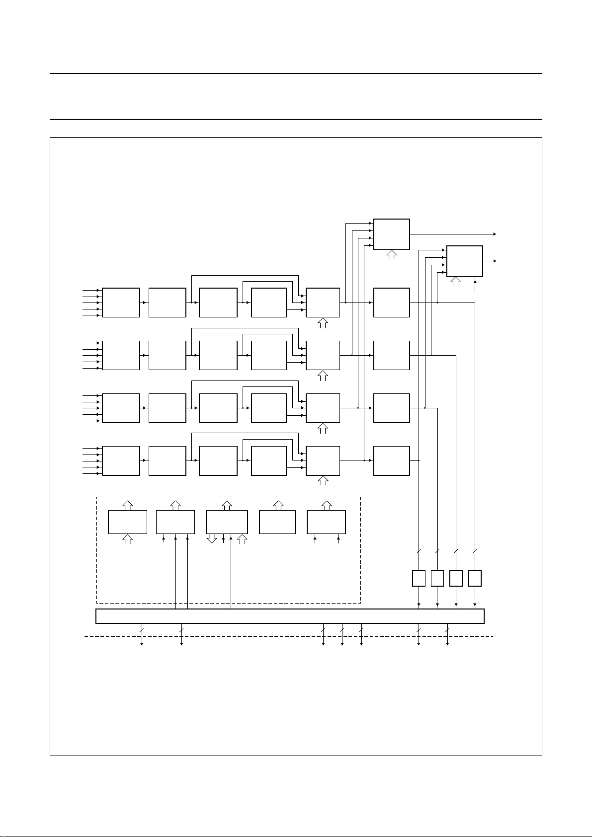
6 BLOCK DIAGRAM
Philips Semiconductors Preliminary specification
Multistandard video decoder with adaptive
comb filter and component video input
FSW
AI11
AI12
AI13
AI14
AI1D
AI21
AI22
AI23
AI24
AI2D
AI31
AI32
AI33
AI34
AI3D
AI41
AI42
AI43
AI44
AI4D
AOUT
AGND
AGNDA
AD PORT
ANALOG1
ADC1
DF
ANALOG2
ADC2
DF
ANALOG3
ADC3
DF
ANALOG4
ADC4
DF
POWER-ON CONTROL
POWER SUPPLY
CONTROL
I2C-BUS REGISTER MAP
FAST SWITCH DELAY
R
G
COMPONENTS
PROCESSING
B
RAW
C
CROMINANCE
PROCESSING
COMB FILTER
ANALOG INPUT CONTROL
Y
LUMININANCE
S
PROCESSING
S
SYNCHRONIZATION VIDEO/TEXT ARBITER
VIDEO
CLOCK
GPO CRYSTAL X PORT
Y
C
B
C
R
C
B
C
R
Y
SS
S
Y-CB-C
R
DECODER OUTPUT CONTROL
RAW
Y-CB-C
R
Y-CB-CRS
FIRST TASK I2C-BUS REGISTER MAP SCALER
SECOND TASK I2C-BUS REGISTER MAP SCALER
SCALER EVENT CONTROLLER
PRESCALER
BCS-SCALER
FIR-PREFILTER
LINE FIFO BUFFER
HORIZONTAL
VERTICAL SCALING
FINE (PHASE) SCALING
SAA7118
VBI-DATA SLICER
CB-C
R
H PORT
CB-C
R
AUDIO
CLOCK
VIDEO FIFO
TEXT
FIFO
BOUNDARY
SCAN
IGP1
IGP0
IGPV
IGPH
]
IPD[7:0
ICLK
IDQ
OUTPUT FORMATTER I PORT
ITRDY
ITRI
V
SSA
V
DDA
V
SSD
V
DDD
V
SS(xtal)
V
DD(xtal)
LLC
LLC2
RTS0
RTS1
RTCO
XTALO
XTALI
XRDY
XTOUT
XCLK
XPD[7:0
Fig.1 Block diagram.
HPD[7:0
AMXCLK
]
XTRIXRH
]
XDQ
XRV
ALRCLK
AMCLK
ASCLK
TDO
TDI TCK
TRST
TMS
SAA7118
Philips Semiconductors Preliminary specification
Multistandard video decoder with adaptive
comb filter and component video input
7 PINNING
SYMBOL
PIN
QFP160 BGA156
DNC6 1 B2 O do not connect, reserved for future extensions and for testing
AI41 2 B1 I analog input 41
AGND 3 C2 P analog ground
V
SSA4
4 C1 P ground for analog inputs AI4x
AI42 5 D2 I analog input 42
AI4D 6 D3 I differential input for ADC channel 4 (pins AI41 to AI44)
AI43 7 D1 I analog input 43
V
DDA4
V
DDA4A
8 D4 P analog supply voltage for analog inputs AI4x (3.3 V)
9 E2 P analog supply voltage for analog inputs AI4x (3.3 V)
AI44 10 E1 I analog input 44
AI31 11 E3 I analog input 31
V
SSA3
12 E4 P ground for analog inputs AI3x
AI32 13 F2 I analog input 32
AI3D 14 F1 I/O differential input for ADC channel 3 (pins AI31 to AI34)
AI33 15 F3 I analog input 33
V
DDA3
V
DDA3A
16 F4 P analog supply voltage for analog inputs AI3x (3.3 V)
17 G2 P analog supply voltage for analog inputs AI3x (3.3 V)
AI34 18 G1 I analog input 34
AI21 19 G4 I analog input 21
V
SSA2
20 H3 P ground for analog inputs AI2x
AI22 21 G3 I analog input 22
AI2D 22 H1 I differential input for ADC channel 2 (pins AI24 to AI21)
AI23 23 H2 I analog input 23
V
DDA2
V
DDA2A
24 H4 P analog supply voltage for analog inputs AI2x
25 J1 P analog supply voltage for analog inputs AI2x
AI24 26 J3 I analog input 24
AI11 27 J2 I analog input 11
V
SSA1
28 J4 P ground for analog inputs AI1x
AI12 29 K1 I analog input 12
AI1D 30 K3 I differential input for ADC channel 1 (pins AI14 to AI11)
AI13 31 K2 I analog input 13
V
DDA1
V
DDA1A
32 K4 P analog supply voltage for analog inputs AI1x (3.3 V)
33 L1 P analog supply voltage for analog inputs AI1x (3.3 V)
AI14 34 L3 I analog input 14
AGNDA 35 L2 P analog signal ground
AOUT 36 M1 O analog test output (do not connect)
V
V
DDA0
SSA0
37 M3 P analog supply voltage (3.3 V) for internal clock generation circuit
38 M2 P ground for internal Clock Generation Circuit (CGC)
TYPE
(1)
DESCRIPTION
SAA7118
2001 May 30 7
Philips Semiconductors Preliminary specification
Multistandard video decoder with adaptive
SAA7118
comb filter and component video input
SYMBOL
PIN
QFP160 BGA156
DNC13 39 N1 NC do not connect, reserved for future extensions and for testing
DNC14 40 N2 I/pu do not connect, reserved for future extensions and for testing
DNC18 41 P2 I/O do not connect, reserved for future extensions and for testing
DNC15 42 N3 I/pd do not connect, reserved for future extensions and for testing
EXMCLR 43 P3 I/pd external mode clear (with internal pull-down)
CE 44 N4 I/pu chip enable or reset input (with internal pull-up)
V
DDD1
45 C5 P digital supply voltage 1 (peripheral cells)
LLC 46 P4 O line-locked system clock output (27 MHz nominal)
V
SSD1
47 D5 P digital ground 1 (peripheral cells)
LLC2 48 N5 O line-locked1⁄2clock output (13.5 MHz nominal)
RES 49 P5 O reset output (active LOW)
V
V
DDD2
SSD2
50 C8 P digital supply voltage 2 (core)
51 D7 P digital ground 2 (core; substrate connection)
CLKEXT 52 N6 I external clock input intended for analog-to-digital conversion of VSB
ADP8 53 P6 O MSB of direct analog-to-digital converted output data (VSB)
ADP7 54 M6 O MSB − 1 of direct analog-to-digital converted output data (VSB)
ADP6 55 L6 O MSB − 2 of direct analog-to-digital converted output data (VSB)
ADP5 56 N7 O MSB − 3 of direct analog-to-digital converted output data (VSB)
ADP4 57 P7 O MSB − 4 of direct analog-to-digital converted output data (VSB)
ADP3 58 L7 O MSB − 5 of direct analog-to-digital converted output data (VSB)
V
DDD3
59 C9 P digital supply voltage 3 (peripheral cells)
ADP2 60 M7 O MSB − 6 of direct analog-to-digital converted output data (VSB)
ADP1 61 P8 O MSB − 7 of direct analog-to-digital converted output data (VSB)
ADP0 62 N8 O LSB of direct analog-to-digital converted output data (VSB)
V
SSD3
63 D9 P digital ground 3 (peripheral cells)
INT_A 64 P9 O/od I2C-bus interrupt flag (LOW if any enabled status bit has changed)
V
DDD4
65 C10 P digital supply voltage 4 (core)
SCL 66 N9 I serial clock input (I2C-bus)
V
SSD4
67 D10 P digital ground 4 (core)
SDA 68 P10 I/O/od serial data input/output (I2C-bus)
RTS0 69 M10 O real-time status or sync information, controlled by subaddresses
RTS1 70 N10 O real-time status or sync information, controlled by subaddresses
RTCO 71 L10 O/st/pd real-time control output; contains information about actual system clock
AMCLK 72 P11 O audio master clock output, up to 50% of crystal clock
TYPE
(1)
DESCRIPTION
signals (36 MHz)
11H and 12H
11H and 12H
frequency, field rate, odd/even sequence, decoder status, subcarrier
frequency and phase and PAL sequence (see document
Description”
, available on request); the RTCO pin is enabled via I2C-bus
“RTC Functional
bit RTCE; see notes 5, 6 and Table 35
2001 May 30 8
Philips Semiconductors Preliminary specification
Multistandard video decoder with adaptive
SAA7118
comb filter and component video input
SYMBOL
PIN
QFP160 BGA156
V
DDD5
73 D12 P digital supply voltage 5 (peripheral cells)
ASCLK 74 N11 O audio serial clock output
ALRCLK 75 P12 O/st/pd audio left/right clock output; can be strapped to supply via a 3.3 kΩ resistor
AMXCLK 76 M12 I audio master external clock input
ITRDY 77 N12 I target ready input for image port data
DNC0 78 P13 I/pu do not connect, reserved for future extensions and for testing: scan input
DNC16 79 N13 NC do not connect, reserved for future extensions and for testing
DNC17 80 N14 NC do not connect, reserved for future extensions and for testing
DNC19 81 − NC do not connect, reserved for future extensions and for testing
DNC20 82 − NC do not connect, reserved for future extensions and for testing
FSW 83 M13 I/pd fast switch (blanking) with internal pull-down inserts component inputs into
ICLK 84 M14 I/O clock output signal for image port, or optional asynchronous back-end
IDQ 85 L13 O output data qualifier for image port (optional: gated clock output)
ITRI 86 L12 I/(O) image port output control signal, affects all input port pins inclusive ICLK,
IGP0 87 L14 O general purpose output signal 0; image port (controlled by subaddresses
V
SSD5
88 D11 P digital ground 5 (peripheral cells)
IGP1 89 K13 O general purpose output signal 1; image port (controlled by subaddresses
IGPV 90 K14 O multi purpose vertical reference output signal; image port (controlled by
IGPH 91 K12 O multi purpose horizontal reference output signal; image port (controlled by
IPD7 92 K11 O MSB of image port data output
IPD6 93 J13 O MSB − 1 of image port data output
IPD5 94 J14 O MSB − 2 of image port data output
V
V
DDD6
SSD6
95 F12 P digital supply voltage 6 (core)
96 F11 P digital ground 6 (core)
IPD4 97 H13 O MSB − 3 of image port data output
IPD3 98 H14 O MSB − 4 of image port data output
IPD2 99 H11 O MSB − 5 of image port data output
IPD1 100 G12 O MSB − 6 of image port data output
V
DDD7
101 H12 P digital supply voltage 7 (peripheral cells)
IPD0 102 G14 O LSB of image port data output
TYPE
(1)
DESCRIPTION
to indicate that the default 24.576 MHz crystal (ALRCLK = 0; internal
pull-down) has been replaced by a 32.110 MHz crystal (ALRCLK = 1);
notes 5 and 7
CVBS signal
clock input
enable and active polarity is under software control (bits IPE in subaddress
87H); output path used for testing: scan output
84H and 85H)
84H and 85H)
subaddresses 84H and 85H)
subaddresses 84H and 85H)
2001 May 30 9
Philips Semiconductors Preliminary specification
Multistandard video decoder with adaptive
SAA7118
comb filter and component video input
SYMBOL
PIN
QFP160 BGA156
HPD7 103 G13 I/O MSB of host port data I/O, extended CB-CR input for expansion port,
V
SSD7
104 G11 P digital ground 7 (peripheral cells)
HPD6 105 F14 I/O MSB − 1 of host port data I/O, extended CB-CR input for expansion port,
V
DDD8
106 J12 P digital supply voltage 8 (core)
HPD5 107 F13 I/O MSB − 2 of host port data I/O, extended CB-CR input for expansion port,
V
SSD8
108 J11 P digital ground 8 (core)
HPD4 109 E14 I/O MSB − 3 of host port data I/O, extended CB-CR input for expansion port,
HPD3 110 E12 I/O MSB − 4 of host port data I/O, extended CB-CR input for expansion port,
HPD2 111 E13 I/O MSB − 5 of host port data I/O, extended CB-CR input for expansion port,
HPD1 112 E11 I/O MSB − 6 of host port data I/O, extended CB-CR input for expansion port,
HPD0 113 D14 I/O LSB of host port data I/O, extended CB-CR input for expansion port,
V
DDD9
114 M4 P digital supply voltage 9 (peripheral cells)
DNC1 115 D13 I/pu do not connect, reserved for future extensions and for testing: scan input
DNC2 116 C14 I/pu do not connect, reserved for future extensions and for testing: scan input
DNC7 117 B13 NC do not connect, reserved for future extensions and for testing
DNC8 118 B14 NC do not connect, reserved for future extensions and for testing
DNC11 119 C12 NC do not connect, reserved for future extensions and for testing
DNC12 120 C13 NC do not connect, reserved for future extensions and for testing
DNC21 121 − NC do not connect, reserved for future extensions and for testing
DNC22 122 − NC do not connect, reserved for future extensions and for testing
DNC3 123 A13 I/pu do not connect, reserved for future extensions and for testing: scan input
DNC4 124 B12 O do not connect, reserved for future extensions and for testing: scan output
DNC5 125 A12 I/pu do not connect, reserved for future extensions and for testing: scan input
XTRI 126 B11 I X-port output control signal, affects all X-port pins (XPD7 to XPD0, XRH,
XPD7 127 C11 I/O MSB of expansion port data
XPD6 128 A11 I/O MSB − 1 of expansion port data
V
SSD9
129 L4 P digital ground 9 (peripheral cells)
XPD5 130 B10 I/O MSB − 2 of expansion port data
XPD4 131 A10 I/O MSB − 3 of expansion port data
V
DDD10
V
SSD10
132 M5 P digital supply voltage 10 (core)
133 L5 P digital ground 10 (core)
TYPE
(1)
DESCRIPTION
extended CB-CR output for image port
extended CB-CR output for image port
extended CB-CR output for image port
extended CB-CR output for image port
extended CB-CR output for image port
extended CB-CR output for image port
extended CB-CR output for image port
extended CB-CR output for image port
XRV, XDQ and XCLK), enable and active polarity is under software control
(bits XPE in subaddress 83H)
2001 May 30 10
Philips Semiconductors Preliminary specification
Multistandard video decoder with adaptive
SAA7118
comb filter and component video input
SYMBOL
PIN
QFP160 BGA156
XPD3 134 B9 I/O MSB − 4 of expansion port data
XPD2 135 A9 I/O MSB − 5 of expansion port data
V
DDD11
V
SSD11
136 M8 P digital supply voltage 11 (peripheral cells)
137 L8 P digital ground 11 (peripheral cells)
XPD1 138 B8 I/O MSB − 6 of expansion port data
XPD0 139 A8 I/O LSB of expansion port data
XRV 140 D8 I/O vertical reference I/O expansion port
XRH 141 C7 I/O horizontal reference I/O expansion port
V
DDD12
142 M9 P digital supply voltage 12 (core)
XCLK 143 A7 I/O clock I/O expansion port
XDQ 144 B7 I/O data qualifier for expansion port
V
SSD12
145 L9 P digital ground 12 (core)
XRDY 146 A6 O task flag or ready signal from scaler, controlled by XRQT
TRST 147 C6 I/pu test reset input (active LOW), for boundary scan test (with internal pull-up);
TCK 148 B6 I/pu test clock for boundary scan test; note 2
TMS 149 D6 I/pu test mode select input for boundary scan test or scan test; note 2
TDO 150 A5 O test data output for boundary scan test; note 2
V
DDD13
151 M11 P digital supply voltage 13 (peripheral cells)
TDI 152 B5 I/pu test data input for boundary scan test; note 2
V
SSD13
V
SS(xtal)
153 L11 P digital ground 13 (peripheral cells)
154 A4 P ground for crystal oscillator
XTALI 155 B4 I input terminal for 24.576 MHz (32.11 MHz) crystal oscillator or connection
XTALO 156 A3 O 24.576 MHz (32.11 MHz) crystal oscillator output; not connected if TTL
V
DD(xtal)
157 B3 P supply voltage for crystal oscillator
XTOUT 158 A2 O crystal oscillator output signal; auxiliary signal
DNC9 159 C3 NC do not connect, reserved for future extensions and for testing
DNC10 160 C4 NC do not connect, reserved for future extensions and for testing
TYPE
(1)
DESCRIPTION
notes 2, 3 and 4
of external oscillator with TTL compatible square wave clock signal
clock input of XTALI is used
Notes
1. I = input, O = output, P = power, NC = not connected, st = strapping, pu = pull-up, pd = pull-down, od = open-drain.
2. In accordance with the
“IEEE1149.1”
standard the pads TDI, TMS, TCK and TRST are input pads with an internal
pull-up transistor and TDO is a 3-state output pad.
3. For board design without boundary scan implementation connect the TRST pin to ground.
4. This pin provides easy initialization of the Boundary Scan Test (BST) circuit. TRST can be used to force the Test
Access Port (TAP) controller to the TEST_LOGIC_RESET state (normal operation) at once.
5. Pin strapping is done by connecting the pin to the supply via a 3.3 kΩ resistor. During the power-up reset sequence
the corresponding pins are switched to input mode to read the strapping level. For the default setting no strapping
resistor is necessary (internal pull-down).
2001 May 30 11
Philips Semiconductors Preliminary specification
Multistandard video decoder with adaptive
SAA7118
comb filter and component video input
6. Pin RTCO operates as I2C-bus slave address pin; RTCO = 0 slave address 42H/43H (default); RTCO = 1 slave
address 40H/41H.
7. Pin ALRCLK: 0 = 24.576 MHz crystal (default); 1 = 32.110 MHz crystal.
handbook, full pagewidth
DD(xtal)
SS(xtal)VSSD13
DNC6
AGND
V
SSA4
AI4D
V
DDA4
V
DDA4A
V
SSA3
AI3D
V
DDA3
V
DDA3A
V
SSA2
AI2D
V
DDA2
V
DDA2A
V
SSA1
AI1D
V
DDA1
V
DDA1A
AGNDA
AOUT
V
DDA0
V
SSA0
DNC13
DNC14
AI41
AI42
AI43
AI44
AI31
AI32
AI33
AI34
AI21
AI22
AI23
AI24
AI11
AI12
AI13
AI14
153
TDI
152
DDD13
V
151
TDO
150
TMS
149
TCK
148
DNC10
DNC9
XTOUT
V
XTALO
XTALI
V
160
159
158
157
156
155
154
1
2
3
4
5
6
7
8
9
10
11
12
13
14
15
16
17
18
19
20
21
22
23
24
25
26
27
28
29
30
31
32
33
34
35
36
37
38
39
40
TRST
147
XRDY
146
SSD12
V
XDQ
145
144
DDD12
XCLK
V
XRH
XRV
143
142
141
140
SAA7118H
XPD0
139
SSD11VDDD11
XPD1
V
138
137
136
XPD2
XPD3
135
134
SSD10VDDD10
V
XPD4
133
132
131
XPD5
130
SSD9
V
129
XPD6
128
XPD7
127
XTRI
126
DNC5
125
DNC4
DNC3
124
123
DNC22
DNC21
122
121
120
119
118
117
116
115
114
113
112
111
110
109
108
107
106
105
104
103
102
101
100
99
98
97
96
95
94
93
92
91
90
89
88
87
86
85
84
83
82
81
DNC12
DNC11
DNC8
DNC7
DNC2
DNC1
V
DDD9
HPD0
HPD1
HPD2
HPD3
HPD4
V
SSD8
HPD5
V
DDD8
HPD6
V
SSD7
HPD7
IPD0
V
DDD7
IPD1
IPD2
IPD3
IPD4
V
SSD6
V
DDD6
IPD5
IPD6
IPD7
IGPH
IGPV
IGP1
V
SSD5
IGP0
ITRI
IDQ
ICLK
FSW
DNC20
DNC19
414243444546474849505152535455565758596061626364656667686970717273747576777879
CE
DNC18
DNC15
EXMCLR
DDD1
V
LLC
SSD1
V
LLC2
RES
DDD2
V
SSD2
V
ADP8
CLKEXT
ADP7
ADP6
ADP5
ADP4
ADP3
DDD3
V
Fig.2 Pin configuration (QFP160).
2001 May 30 12
ADP2
ADP1
ADP0
SSD3
V
INT_A
V
SCL
DDD4
SSD4
V
SDA
RTS0
RTS1
RTCO
DDD5
V
AMCLK
ASCLK
ALRCLK
ITRDY
AMXCLK
DNC0
80
DNC16
DNC17
MXXxxx

Philips Semiconductors Preliminary specification
Multistandard video decoder with adaptive
comb filter and component video input
handbook, halfpage
P
N
M
L
K
J
H
G
F
E
D
C
B
A
1
234567891011121314
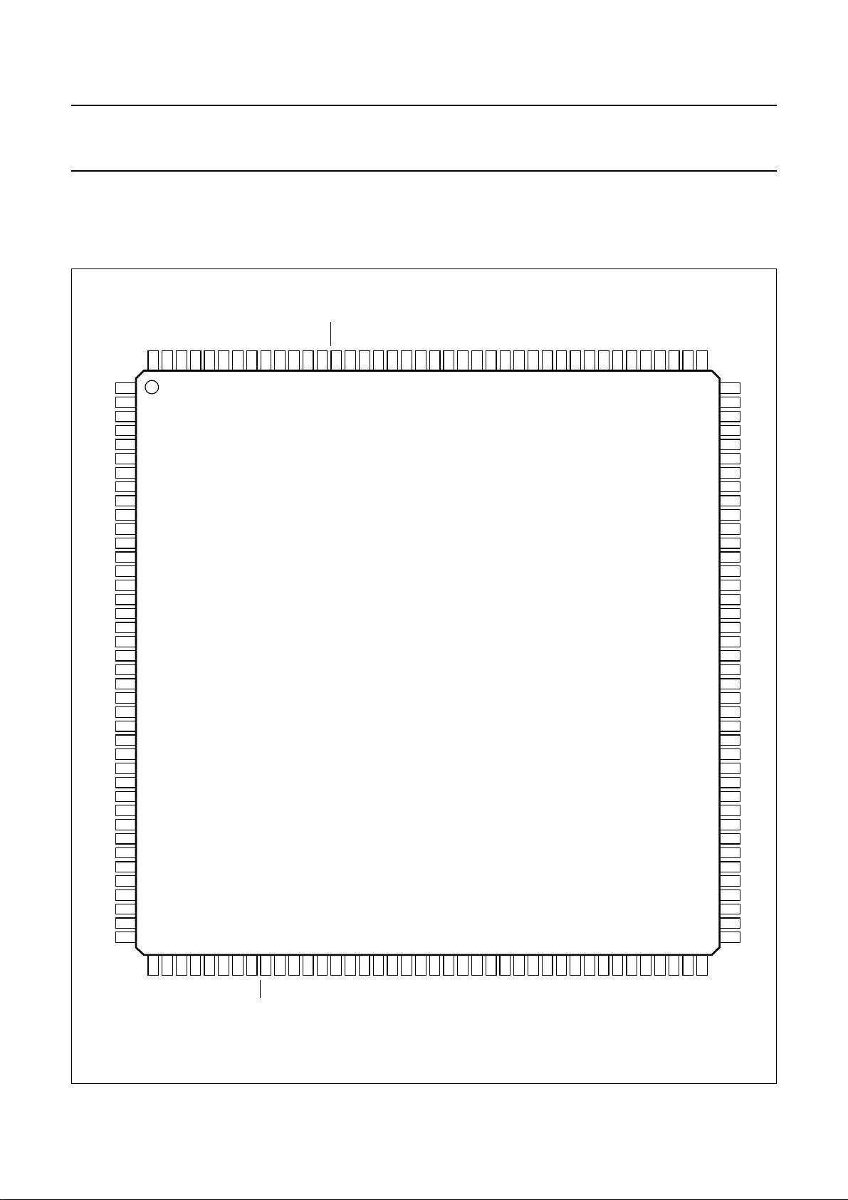
Fig.3 Pin configuration (BGA156).
SAA7118E
SAA7118
MHB725
2001 May 30 13

2001 May 30 14
Table 1 Pin assignment (top view)
1234567891011121314
Philips Semiconductors Preliminary specification
Multistandard video decoder with adaptive
comb filter and component video input
A XTOUT XTALO V
B AI41 TEST3 V
C V
SSA4
AGND TEST7 TEST8 V
DD(xtal)
D AI43 AI42 AI4D V
E AI44 V
DDA4A
AI31 V
F AI3D AI32 AI33 V
G AI34 V
DDA3A
H AI2D AI23 V
J V
DDA2A
AI11 AI24 V
AI22 AI21 V
SSA2
K AI12 AI13 AI1D V
SS(xtal)
TDO XRDY XCLK XPD0 XPD2 XPD4 XPD6 TEST1 TEST2
XTALI TDI TCK XDQ XPD1 XPD3 XPD5 XTRI TEST4 TEST5 TEST6
V
DDA4
SSA3
DDA3
DDA2
SSA1
DDA1
V
DDD1
SSD1
TRST XRH V
TMS V
SSD2
DDD2
XRV V
V
DDD3
SSD3
V
V
DDD4
SSD4
XPD7 TEST9 TEST10 TEST11
V
SSD5
V
DDD5
TEST12 HPD0
HPD1 HPD3 HPD2 HPD4
V
SSD6
SSD7
IPD2 V
V
SSD8
V
DDD6
HPD5 HPD6
IPD1 HPD7 IPD0
IPD4 IPD3
IPD6 IPD5
V
DDD7
DDD8
IPD7 IGPH IGP1 IGPV
L V
DDA1A
M AOUT V
AGNDA AI14 V
SSA0
V
DDA0
V
SSD9
DDD9
V
SSD10
V
DDD10
ADP6 ADP3 V
ADP7 ADP2 V
SSD11VSSD12
DDD11VDDD12
RTCO V
RTS0 V
SSD13
DDD13
ITRI IDQ IGP0
AMXCLK FSW ICLK
N TEST13 TEST14 TEST15 CE LLC2 CLKEXT ADP5 ADP0 SCL RTS1 ASCLK ITRDY TEST16 TEST17
P TEST18 EXMCLR LLC RES ADP8 ADP4 ADP1 INT_A SDA AMCLK ALRCLK TEST19
SAA7118

2001 May 30 15
Table 2 8-bit/16-bit and alternative pin functional configurations
(1)
PIN
C11,
A11,
B10,
A10, B9,
A9, B8,
A8 (127,
128,130,
131,134,
135,138,
139)
A7 (143) XCLK clock
B7 (144) XDQ data
A6 (146) XRDY input
C7 (141) XRH horizontal
D8 (140) XRV vertical
B11
(126)
SYMBOL
XPD7 to
XPD0
XTRI output
8-BIT
INPUT
MODES
D1 data
input
input
qualifier
input
ready
output
reference
input
reference
input
enable
input
16-BIT INPUT
MODES (ONLY
FOR I2C-BUS
PROGRAMMING)
Y data input D1
ALTERNATIVE
INPUT
FUNCTIONS
gated clock
input
active task A/B
flag
8-BIT
OUTPUT
MODES
decoder
output
decoder
clock
output
data
qualifier
output
(HREFand
VREF
gate)
decoder
horizontal
reference
output
decoder
vertical
reference
output
16-BIT OUTPUT
MODES (ONLY
FOR I2C-BUS
PROGRAMMING)
ALTERNATIVE
OUTPUT
FUNCTIONS
I/O
CONFIGURATION
PROGRAMMING
BITS
XCODE[92H[3]]
XPE[1:0] 83H[1:0]
+ pin XTRI
XPE[1:0] 83H[1:0]
+ pin XTRI
XPCK[1:0] 83H[5:4]
XCKS[92H[0]]
XDQ[92H[1]]
XPE[1:0] 83H[1:0]
+ pin XTRI
XRQT[83H[2]]
XPE[1:0] 83H[1:0]
+ pin XTRI
XDH[92H[2]]
XPE[1:0] 83H[1:0]
+ pin XTRI
XDV[1:0] 92H[5:4]
XPE[1:0] 83H[1:0]
+ pin XTRI
XPE[1:0] 83H[1:0]
Philips Semiconductors Preliminary specification
Multistandard video decoder with adaptive
comb filter and component video input
SAA7118

2001 May 30 16
(1)
PIN
G13,
F14,
F13,
E14,
E12,
E13,
E11,D14
(103,
105,107,
109 to
113)
K11,
J13,J14,
H13,
H14,
H11,
G12,
G14 (92
to 94, 97
to 99,
100,
102)
M14 (84) ICLK clock
L13 (85) IDQ data
N12 (77) ITRDY target
K12 (91) IGPH H-gate
SYMBOL
HPD7 to
HPD0
IPD7 to
IPD0
8-BIT
INPUT
MODES
16-BIT INPUT
MODES (ONLY
FOR I2C-BUS
PROGRAMMING)
CB-CR data input CB-CR scaler
ALTERNATIVE
INPUT
FUNCTIONS
8-BIT
OUTPUT
MODES
D1 scaler
output
output
qualifier
output
ready input
output
16-BIT OUTPUT
MODES (ONLY
FOR I2C-BUS
PROGRAMMING)
output
Y scaler output ICODE[93H[7]]
ALTERNATIVE
OUTPUT
FUNCTIONS
clock input ICKS[1:0] 80H[1:0]
gated clock
output
extended
H-gate,
horizontal
pulses
CONFIGURATION
PROGRAMMING
ICODE[93H[7]]
ISWP[1:0] 85H[7:6]
I8_16[93H[6]]
IPE[1:0] 87H[1:0]
+ pin ITRI
ISWP[1:0] 85H[7:6]
I8_16[93H[6]]
IPE[1:0] 87H[1:0]
+ pin ITRI
IPE[1:0] 87H[1:0]
+ pin ITRI
ICKS[3:2] 80H[3:2]
IDQP[85H[0]]
IPE[1:0] 87H[1:0]
+ pin ITRI
IDH[1:0] 84H[1:0]
IRHP[85H[1]]
IPE[1:0] 87H[1:0]
+ pin ITRI
I/O
BITS
Philips Semiconductors Preliminary specification
Multistandard video decoder with adaptive
comb filter and component video input
SAA7118

2001 May 30 17
(1)
PIN
K14 (90) IGPV V-gate
K13 (89) IGP1 general
L14 (87) IGP0 general
L12 (86) ITRI output
Note
1. Pin numbers for QFP160 in parenthesis.
SYMBOL
8-BIT
INPUT
MODES
16-BIT INPUT
MODES (ONLY
FOR I2C-BUS
PROGRAMMING)
ALTERNATIVE
INPUT
FUNCTIONS
8-BIT
OUTPUT
MODES
output
purpose
purpose
enable
input
16-BIT OUTPUT
MODES (ONLY
FOR I2C-BUS
PROGRAMMING)
ALTERNATIVE
OUTPUT
FUNCTIONS
V-sync, vertical
pulses
I/O
CONFIGURATION
PROGRAMMING
BITS
IDV[1:0] 84H[3:2]
IRVP[85H[2]]
IPE[1:0] 87H[1:0]
+ pin ITRI
IDG1[1:0] 84H[5:4]
IG1P[85H[3]]
IPE[1:0] 87H[1:0]
+ pin ITRI
IDG0[1:0] 84H[7:6]
IG0P[85H[4]]
IPE[1:0] 87H[1:0]
+ pin ITRI
Philips Semiconductors Preliminary specification
Multistandard video decoder with adaptive
comb filter and component video input
SAA7118
Philips Semiconductors Preliminary specification
Multistandard video decoder with adaptive
SAA7118
comb filter and component video input
8 FUNCTIONAL DESCRIPTION
8.1 Decoder
8.1.1 ANALOG INPUT PROCESSING
The SAA7118 offers sixteen analog signal inputs, four analog main channels with source switch, clamp circuit, analog
amplifier, anti-alias filter and video 9-bit CMOS ADC with a Decimation Filter (DF); see Figs 5 and 8.
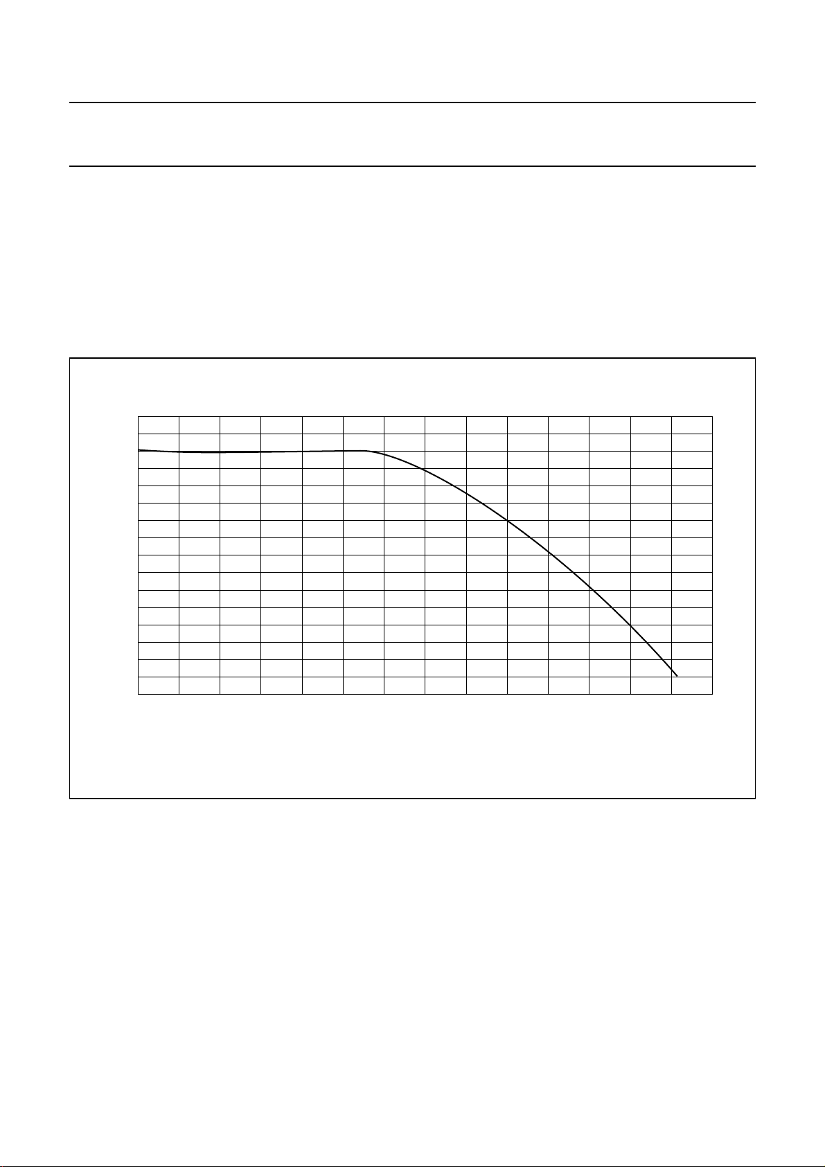
The anti-alias filters are adapted to the line-locked clock frequency via a filter control circuit. The characteristic is shown
in Fig.4. During the vertical blanking period gain and clamping control are frozen.
MGD138
V
(dB)
6
0
−6
−12
−18
−24
−30
−36
−42
024 68101214
f (MHz)
Fig.4 Anti-alias filter.
2001 May 30 18
Philips Semiconductors Preliminary specification
Multistandard video decoder with adaptive
comb filter and component video input
3
gain
(dB)
0
−3
−6
−9
−12
−15
−18
−21
−24
−27
−30
−33
−36
−39
−42
−45
−48
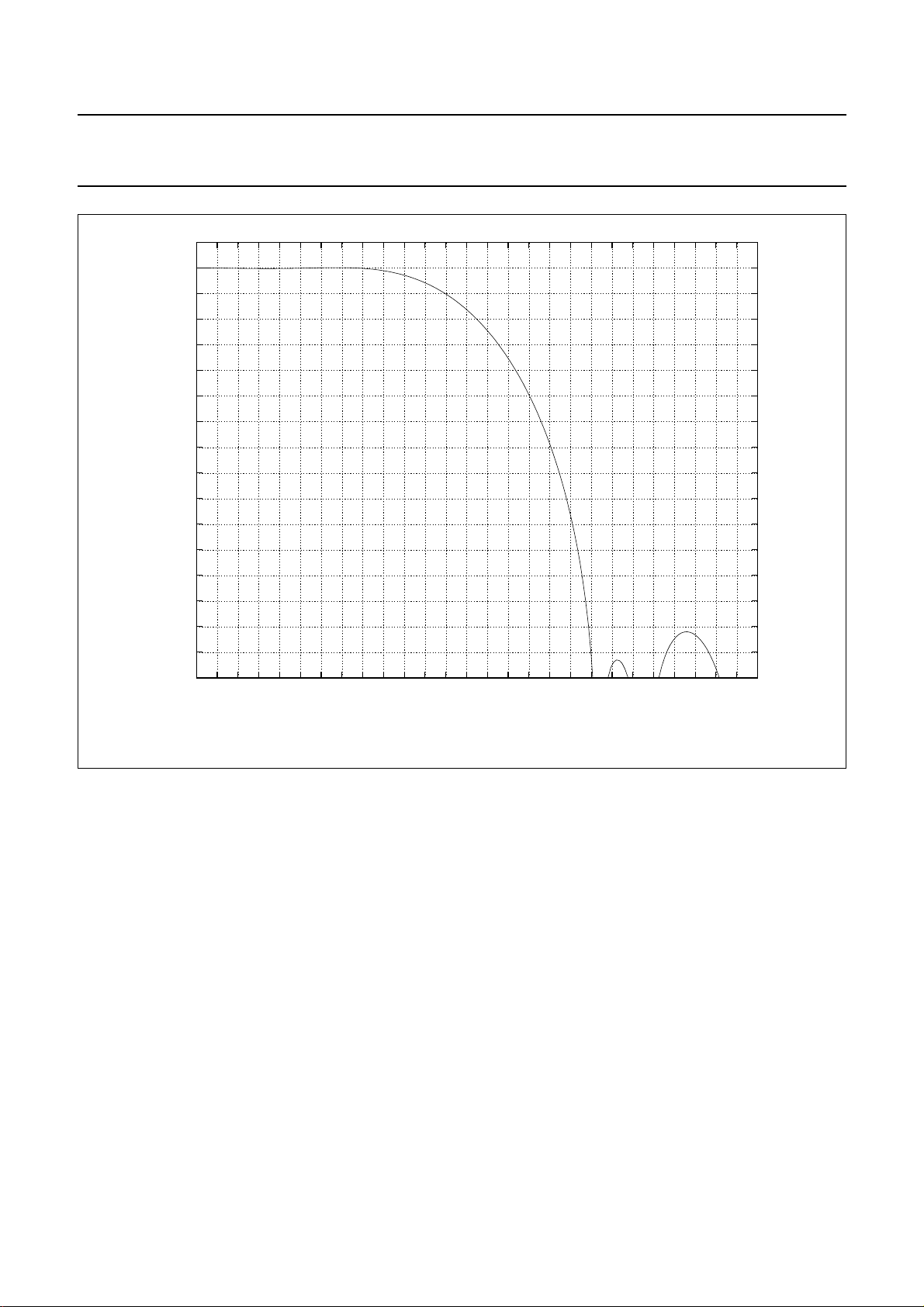
0 0.5 1 1.5 2 2.5 3 3.5 4 4.5 5 5.5 6 6.5 7 7.5 8 8.5 9 9.5 10 10.5 11 11.5 12 12.5 13 13.5
SAA7118
f (MHz)
Fig.5 Decimation filter.
2001 May 30 19
Philips Semiconductors Preliminary specification
Multistandard video decoder with adaptive
comb filter and component video input
8.1.1.1 Clamping
The clamp control circuit controls the correct clamping of
the analog input signals. The coupling capacitor is also
used to store and filter the clamping voltage. An internal
digital clamp comparator generates the information with
respect to clamp-up or clamp-down. The clamping levels
for the four ADC channels are fixed for luminance (120),
chrominance (256) and for component inputs as
component Y (32), components PB and PR (256) or
components RGB (32). Clamping time in normaluse is set
with the HCL pulse on the back porch of the video signal.
8.1.1.2 Gain control
The gain control circuit receives (via theI2C-bus) the static
gain levels for the four analog amplifiers or controls one of
theseamplifiersautomaticallyviaabuilt-inAutomaticGain
Control (AGC) as part of the Analog Input Control (AICO).
SAA7118
The AGC (automatic gain control for luminance) is used to
amplify a CVBS or Y signal to the required signal
amplitude, matched to the ADCs input voltage range.
Component inputs are gain adjusted manually at a fixed
gain. The AGC active time is the sync bottom of the video
signal.
Signal (white) peak control limits the gain at signal
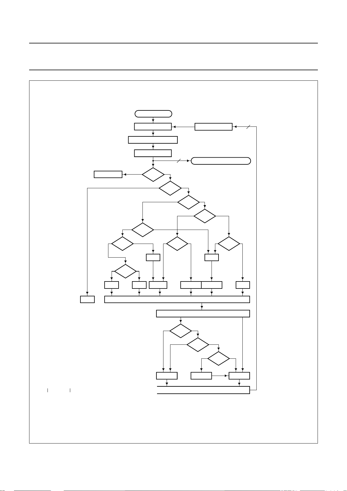
overshoots. The flow charts (see Figs 9 and 10) show
more details of the AGC. The influence of supply voltage
variation within the specified range is automatically
eliminated by clamp and automatic gain control.
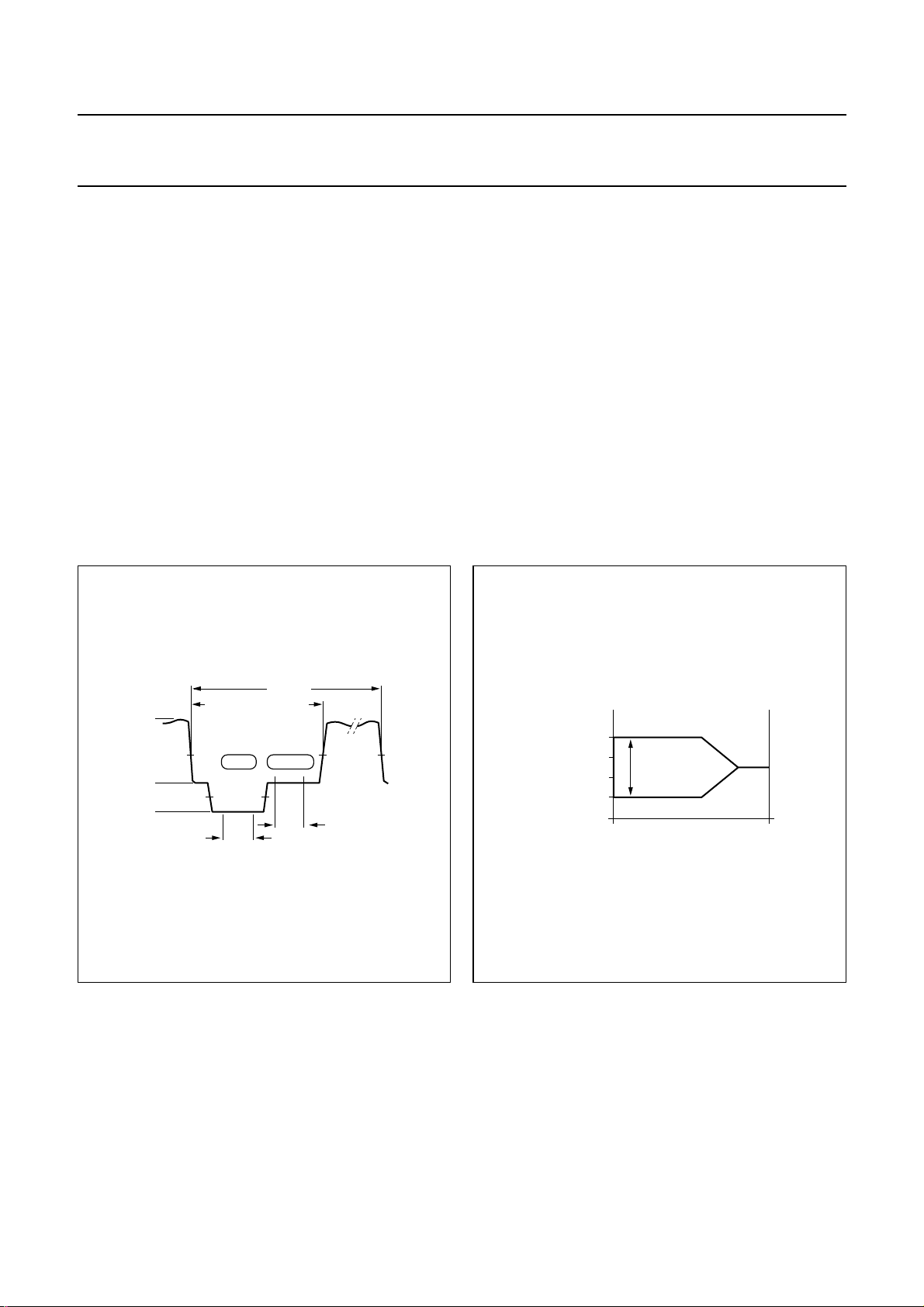
handbook, halfpage
analog line blanking
511
GAIN CLAMP
120
1
TV line
HCL
HSY
Fig.6 Analog line with clamp (HCL) and gain
range (HSY). Fig.7 Automatic gain range.
MHB726
analog input level
+3 dB
0 dB
(1 V (p-p) 18/56 Ω)
−6 dB
maximum
range 9 dB
minimum
controlled
ADC input level
0 dB
MHB325
2001 May 30 20
Philips Semiconductors Preliminary specification
Multistandard video decoder with adaptive
comb filter and component video input
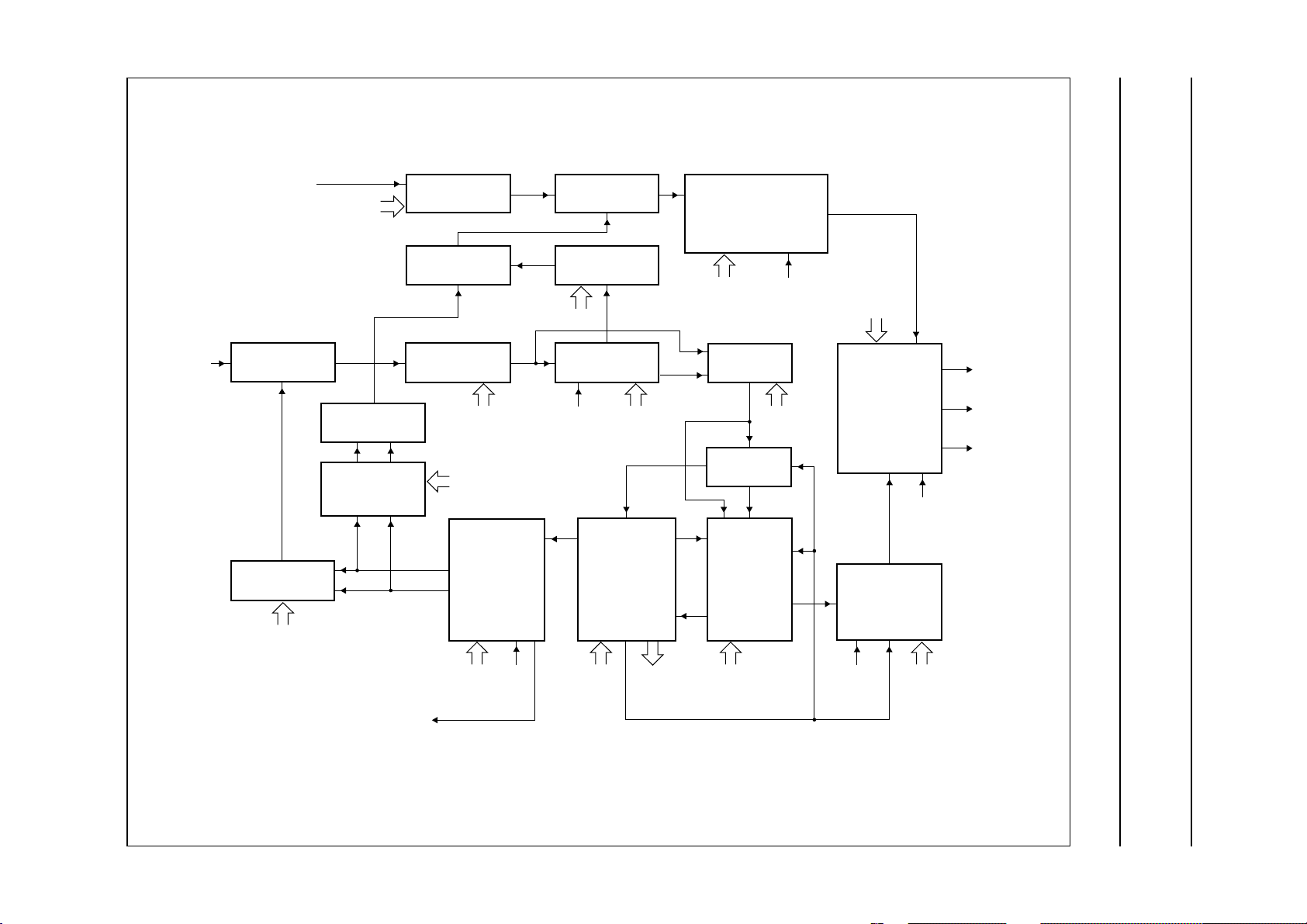
handbook, full pagewidth
AI44
AI43
AI42
AI41
AI4D
AI34
AI33
AI32
AI31
AI3D
SOURCE
SWITCH
SOURCE
SWITCH
CLAMP
CIRCUIT
CLAMP
CIRCUIT
ANALOG
AMPLIFIER
DAC9
ANALOG
AMPLIFIER
DAC9
ANTI-ALIAS
FILTER
ANTI-ALIAS
FILTER
BYPASS
SWITCH
FUSE[1:0
BYPASS
SWITCH
SAA7118
TEST
SELECTOR
AND
BUFFER
DIGITAL
]
AOSL[2:0
ADC4
]
ADC3
TEST
SELECTOR
DOSL[1:0
]
ADPE
AOUT
ADP[8:0
]
AI24
AI23
AI22
AI21
AI2D
AI14
AI13
AI12
AI11
AI1D
SOURCE
SWITCH
SOURCE
SWITCH
MODE
CONTROL
MODE[5:0
]
FUSE[1:0
CLAMP
CIRCUIT
CLAMP
CIRCUIT
CLAMP
CONTROL
HCL
]
CHROMACVBS/Y
ANALOG
AMPLIFIER
DAC9
ANALOG
AMPLIFIER
DAC9
GLIMB
GLIMT
WIPA
SLTCA
GAIN
CONTROL
HSY
HOLDG
GAFIX
WPOFF
GUDL[1:0
GAI[48:40
GAI[38:30
HLNRS
UPTCV
REFA
ANTI-ALIAS
ANTI-ALIAS
FILTER
FILTER
ANTI-ALIAS
CONTROL
VBSL
]
]
]
ANALOG CONTROL
CROSS MULTIPLEXER
BYPASS
SWITCH
FUSE[1:0
BYPASS
SWITCH
FUSE[1:0
VERTICAL
BLANKING
CONTROL
9
R/R - Y
]
]
VBLNK
SVREF
G/Y
9
9
B/B - Y
ADC2
ADC1
99
DF DF DF DF
9999
9
AD1/3BYPAD2/4BYP
9
Fig.8 Analog input processing using the SAA7118 as differential front-end with 9-bit ADC.
2001 May 30 21
Philips Semiconductors Preliminary specification
Multistandard video decoder with adaptive
comb filter and component video input
handbook, full pagewidth
NO ACTION
ANALOG INPUT
AMPLIFIER
ANTI-ALIAS FILTER
ADC
1
VBLK
1
0
HOLDG
SAA7118
gain
9
0
1
X
1
DAC
LUMA/CHROMA DECODER
0
0
HSY
9
STOP
X = system variable.
Y AGV FGV– GUDL>=
GUDL = gain update level (adjustable).
VBLK = vertical blanking pulse.
HSY = horizontal sync pulse.
AGV = actual gain value.
FGV = frozen gain value.
.
1
+1/F
0
10
<
4
>
496
+1/L
1
>
510
10
<
1
X = 0
0
−1/LLC2
GAIN ACCUMULATOR (18 BITS)
ACTUAL GAIN VALUE 9-BIT (AGV) [−3/+6 dB
AGV
+1/LLC2 −1/LLC2
1
X
1
GAIN VALUE 9-BIT
0
HSY
UPDATE
10
>
510
X = 1
+/− 0
0
1
0
Y
FGV
MHB728
]
Fig.9 Gain flow chart.
2001 May 30 22
Philips Semiconductors Preliminary specification
Multistandard video decoder with adaptive
comb filter and component video input
ANALOG INPUT
ADC
NO BLANKING ACTIVE
10 10
10
CLL
+ CLAMP − CLAMP
10
VBLK
HCL HSY
01 10
NO CLAMP
+ GAIN − GAIN
GAIN -><- CLAMP
SBOT
fast − GAIN
SAA7118
WIPE
slow + GAIN
MGC647
WIPE = white peak level (510).
SBOT = sync bottom level (1).
CLL = clamp level [120 for CVBS, Y(C), S; 256 for C(Y), PB-PR; 32 for RGB, Y].
HSY = horizontal sync pulse.
HCL = horizontal clamp pulse.
Fig.10 Clamp and gain flow chart.
2001 May 30 23
This text is here in white to force landscape pages to be rotated correctly when browsing through the pdf in the Acrobat reader.This text is here in
a
_white to force landscape pages to be rotated correctly when browsing through the pdf in the Acrobat reader.This text is here inThis text is here in
white to force landscape pages to be rotated correctly when browsing through the pdf in the Acrobat reader. white to force landscape pages to be ...
2001 May 30 24
ndbook, full pagewidth
8.1.2 CHROMINANCE AND LUMINANCE PROCESSING
Philips Semiconductors Preliminary specification
Multistandard video decoder with adaptive
comb filter and component video input
CVBS-IN
or CHR-IN
CVBS-IN
or Y-IN
QUADRATURE
DEMODULATOR
SUBCARRIER
GENERATION 1
HUEC
LDEL
YCOMB
SUBCARRIER
GENERATION 2
CHROMINANCE
INCREMENT
DELAY
DELAY
COMPENSATION
QUADRATURE
MODULATOR
LOW-PASS 1
DOWNSAMPLING
LCBW[2:0
LDEL
YCOMB
CHROMINANCE
INCREMENT
DTO RESET
SUBCARRIER
INCREMENT
GENERATION
AND
DIVIDER
]
CHR
CB-C
SUBTRACTOR
R
INTERPOLATION
LOW-PASS 3
LUBW
ADAPTIVE
COMB FILTER
SET_RAW
SET_VBI
DEMODULATOR
AMPLITUDE
DETECTOR
BURST GATE
ACCUMULATOR
LOOP FILTER
CB-C
CCOMB
YCOMB
LDEL
BYPS
PHASE
Y
LUMINANCE-PEAKING
Y-DELAY ADJUSTMENT
LUFI[3:0
CSTD[2:0
CB-C
YDEL[2:0
R
R
OR
LOW-PASS,
]
SET_RAW
]
SET_VBI
]
LOW-PASS 2
CHBW
SECAM
PROCESSING
CHROMA
GAIN
CONTROL
CB-C
ADJUSTMENT
R
Y/CVBS
]
DBRI[7:0
DCON[7:0
DSAT[7:0
RAWG[7:0
RAWO[7:0
CB-C
PAL DELAY LINE
RECOMBINATION
]
]
]
]
COLO
BRIGHTNESS
CONTRAST
SATURATION
CONTROL
RAW DATA
GAIN AND
OFFSET
CONTROL
SET_RAW
R
SET_VBI
SECAM
Y-OUT/
CVBS OUT
CB-CR-OUT
HREF-OUT
CDTO
RTCO
CSTD[2:0
INCS
]
FCTC
ACGC
CGAIN[6:0
IDEL[3:0
CODE
]
]
Fig.11 Chrominance and luminance processing.
SECS
SET_RAW
SET_VBI
fH/2 switch signal
DCVF
MHB729
SAA7118

Philips Semiconductors Preliminary specification
Multistandard video decoder with adaptive
comb filter and component video input
8.1.2.1 Chrominance path
The 9-bit CVBS or chrominance input signal is fed to the
inputofa quadrature demodulator, where it is multiplied by
twotime-multiplexed subcarrier signalsfromthe subcarrier
generation block 1 (0° and 90° phase relationship to the
demodulator axis). The frequency is dependent on the
chosen colour standard.
The time-multiplexed output signals of the multipliers are
low-pass filtered (low-pass 1). Eight characteristics are
programmable via LCWB3 to LCWB0 to achieve the
desired bandwidth for the colour difference signals (PAL,
NTSC) or the 0° and 90° FM signals (SECAM).
Thechrominance low-pass 1characteristicalso influences
the grade of cross-luminance reduction during horizontal
colour transients (large chrominance bandwidth means
strong suppression of cross-luminance). If the Y-comb
filterisdisabledbyYCOMB = 0 the filter influences directly
the width of the chrominance notch within the luminance
path (a large chrominance bandwidth means wide
chrominance notch resulting in a lower luminance
bandwidth).
The low-pass filtered signals are fed to the adaptive comb
filter block. The chrominance components are separated
from the luminance via a two line vertical stage (four lines
for PAL standards) and a decision logic between the
filtered and the non-filtered output signals. This block is
bypassed for SECAM signals. The comb filter logic can be
enabled independently for the succeeding luminance and
chrominance processing by YCOMB (subaddress 09H,
bit 6) and/or CCOMB (subaddress 0EH, bit 0). It is always
bypassed during VBI or raw data lines programmable by
the LCRn registers (subaddresses 41H to 57H); see
Section 8.3.
The separated CB-CR components are further processed
by a second filter stage (low-pass 2) to modify the
chrominance bandwidth without influencing the luminance
path. It’s characteristic is controlled by CHBW
(subaddress 10H, bit 3). For the complete transfer
characteristic of low-passes 1 and 2 see Figs 12 and 13.
SAA7118
The succeeding chrominance gain control block amplifies
or attenuates the CB-CR signal according to the required
ITU 601/656 levels. It is controlled by the output signal
from the amplitude detection circuit within the burst
processing block.
The burst processing block provides the feedback loop of
the chrominance PLL and contains the following:
• Burst gate accumulator
• Colour identification and colour killer
• Comparisonnominal/actual burstamplitude(PAL/NTSC
standards only)
• Loop filter chrominance gain control (PAL/NTSC
standards only)
• Loop filter chrominance PLL (only active for PAL/NTSC
standards)
• PAL/SECAM sequence detection, H/2-switch
generation.
The increment generation circuit produces the Discrete
Time Oscillator (DTO) increment for both subcarrier
generation blocks. It contains a division by the increment
of the line-locked clock generator to create a stable
phase-locked sine signal under all conditions (e.g. for
non-standard signals).
The PAL delay line block eliminates crosstalk between the
chrominance channels in accordance with the PAL
standard requirements. For NTSC colour standards the
delay line can be used as an additional vertical filter.
If desired, it can be switched off by DCVF = 1. It is always
disabledduringVBIorrawdata lines programmable by the
LCRn registers (subaddresses 41H to 57H); see
Section 8.3. The embedded line delay is also used for
SECAM recombination (cross-over switches).
The SECAM processing (bypassed for QAM standards)
contains the following blocks:
• Baseband ‘bell’ filters to reconstruct the amplitude and
phase equalized 0° and 90° FM signals
• Phase demodulator and differentiator
(FM-demodulation)
• De-emphasis filter to compensate the pre-emphasized
input signal, including frequency offset compensation
(DB or DR white carrier values are subtracted from the
signal, controlled by the SECAM switch signal).
2001 May 30 25
Philips Semiconductors Preliminary specification
Multistandard video decoder with adaptive
comb filter and component video input
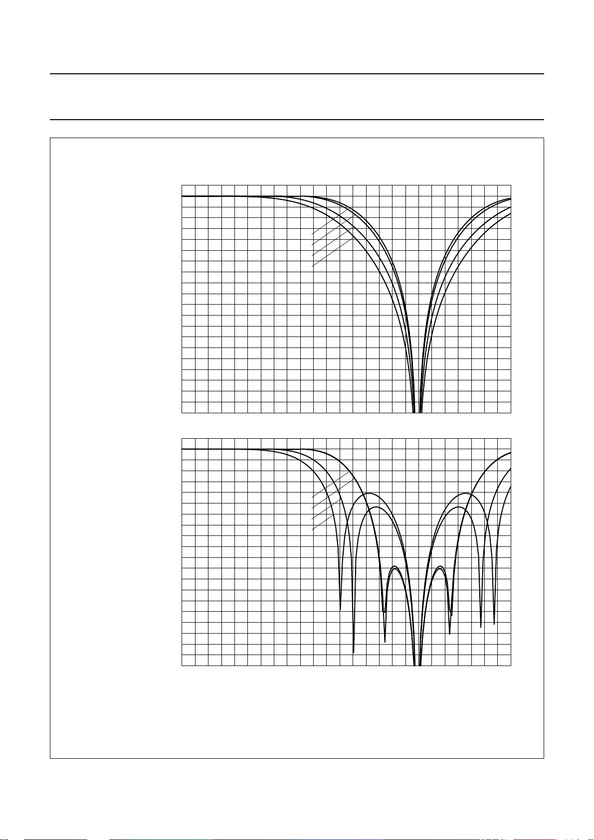
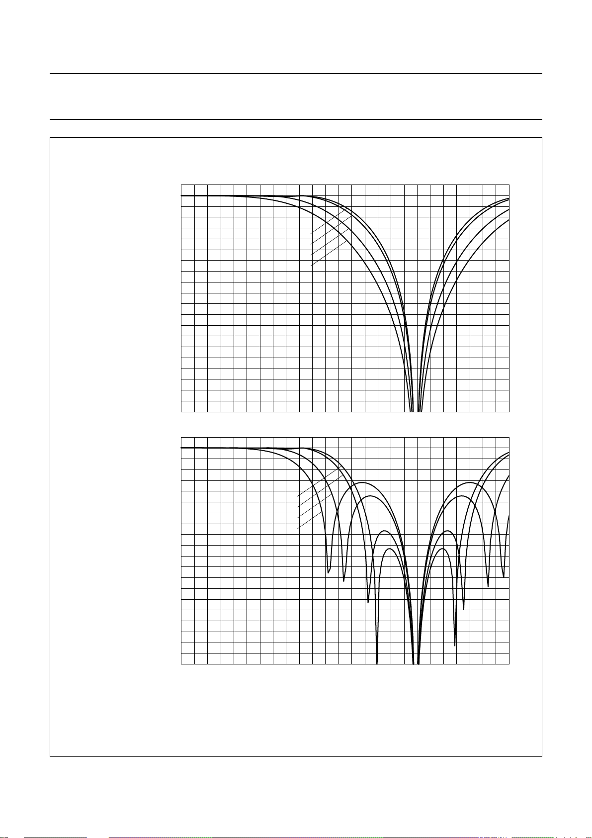
3
V
0
(dB)
−3
−6
−9
(1) LCBW[2:0] = 000.
(2) LCBW[2:0] = 010.
(3) LCBW[2:0] = 100.
(4) LCBW[2:0] = 110.
(5) LCBW[2:0] = 001.
(6) LCBW[2:0] = 011.
(7) LCBW[2:0] = 101.
(8) LCBW[2:0] = 111.
−12
−15
−18
−21
−24
−27
−30
−33
−36
−39
−42
−45
−48
−51
−54
−57
−60
0 0.2 0.4 0.6 0.8 1.0 1.2 1.4 1.6 1.8 2.0 2.2 2.4 2.6 2.8 3.0 3.2 3.4 3.6 3.8 4.0
3
V
0
(dB)
−3
−6
−9
−12
−15
−18
−21
−24
−27
−30
−33
−36
−39
−42
−45
−48
−51
−54
−57
−60
0 0.2 0.4 0.6 0.8 1.0 1.2 1.4 1.6 1.8 2.0 2.2 2.4 2.6 2.8 3.0 3.2 3.4 3.6 3.8 4.0
(1)
(2)
(3)
(4)
(5)
(6)
(7)
(8)
SAA7118
MHB533
f (MHz)
f (MHz)
Fig.12 Transfer characteristics of the chrominance low-pass at CHBW = 0.
2001 May 30 26
Philips Semiconductors Preliminary specification
Multistandard video decoder with adaptive
comb filter and component video input
3
V
0
(dB)
−3
−6
−9
(1) LCBW[2:0] = 000.
(2) LCBW[2:0] = 010.
(3) LCBW[2:0] = 100.
(4) LCBW[2:0] = 110.
(5) LCBW[2:0] = 001.
(6) LCBW[2:0] = 011.
(7) LCBW[2:0] = 101.
(8) LCBW[2:0] = 111.
−12
−15
−18
−21
−24
−27
−30
−33
−36
−39
−42
−45
−48
−51
−54
−57
−60
0 0.2 0.4 0.6 0.8 1.0 1.2 1.4 1.6 1.8 2.0 2.2 2.4 2.6 2.8 3.0 3.2 3.4 3.6 3.8 4.0
3
V
0
(dB)
−3
−6
−9
−12
−15
−18
−21
−24
−27
−30
−33
−36
−39
−42
−45
−48
−51
−54
−57
−60
0 0.2 0.4 0.6 0.8 1.0 1.2 1.4 1.6 1.8 2.0 2.2 2.4 2.6 2.8 3.0 3.2 3.4 3.6 3.8 4.0
(1)
(2)
(3)
(4)
(5)
(6)
(7)
(8)
SAA7118
MHB534
f (MHz)
f (MHz)
Fig.13 Transfer characteristics of the chrominance low-pass at CHBW = 1.
2001 May 30 27

Philips Semiconductors Preliminary specification
Multistandard video decoder with adaptive
comb filter and component video input
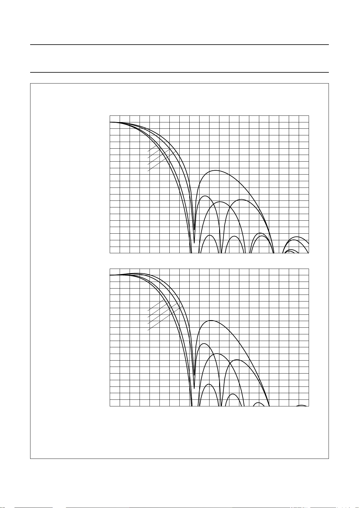
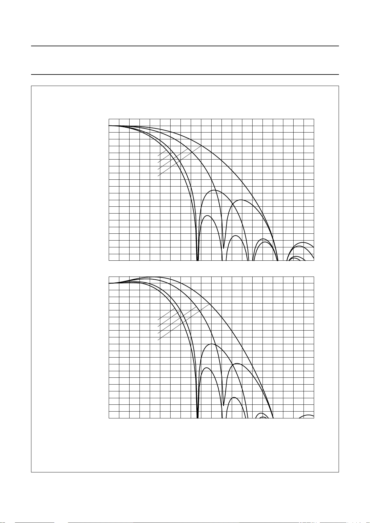
8.1.2.2 Luminance path
The rejection of the chrominance components within the
9-bit CVBS or Y input signal isachieved by subtracting the
remodulated chrominance signal from the CVBS input.
The comb filtered CB-CR components are interpolated
(upsampled) by the low-pass 3 block. It’s characteristic is
controlled by LUBW (subaddress 09H, bit 4) to modify the
width of the chrominance ‘notch’ without influencing the
chrominance path. The programmable frequency
characteristics available, in conjunction with the LCBW2
to LCBW0 settings, can be seen in Figs 14 to 17. It should
be noted that these frequency curves are only valid for
Y-comb disabled filter mode (YCOMB = 0). In comb filter
modethe frequency response is flat. The centre frequency
of the notch is automatically adapted to the chosen colour
standard.
The interpolated CB-CR samples are multiplied by two
time-multiplexed subcarrier signals from the subcarrier
generation block 2. This second DTO is locked to the first
subcarrier generator by an increment delay circuit
matchedtotheprocessingdelay,which is different for PAL
and NTSC standards according to the chosen comb filter
algorithm. The two modulated signals are finally added to
build the remodulated chrominance signal.
SAA7118
The frequency characteristic of the separated luminance
signal can be further modified by the succeeding
luminance filter block. It can be configured as peaking
(resolution enhancement) or low-pass block by LUFI3 to
LUFI0 (subaddress 09H, bits 3 to 0). The 16 resulting
frequency characteristics can be seen in Fig.18. The
LUFI3 to LUFI0 settings can be used as a user
programmable sharpness control.
The luminance filter block also contains the adjustable
Y-delay part; programmable by YDEL2 to YDEL0
(subaddress 11H, bits 2 to 0).
2001 May 30 28
Philips Semiconductors Preliminary specification
Multistandard video decoder with adaptive
comb filter and component video input
3
V
0
(dB)
−3
−6
(1) LCBW[2:0] = 000.
(2) LCBW[2:0] = 010.
(3) LCBW[2:0] = 100.
(4) LCBW[2:0] = 110.
(5) LCBW[2:0] = 001.
(6) LCBW[2:0] = 011.
(7) LCBW[2:0] = 101.
(8) LCBW[2:0] = 111.
−9
−12
−15
−18
−21
−24
−27
−30
−33
−36
−39
−42
−45
−48
−51
−54
−57
−60
0 0.2 0.4 0.6 0.8 1.0 1.2 1.4 1.6 1.8 2.0 2.2 2.4 2.6 2.8 3.0 3.2 3.4 3.6 3.8 4.0 4.2 4.4 4.6 4.8 5.0
3
V
0
(dB)
−3
−6
−9
−12
−15
−18
−21
−24
−27
−30
−33
−36
−39
−42
−45
−48
−51
−54
−57
−60
0 0.2 0.4 0.6 0.8 1.0 1.2 1.4 1.6 1.8 2.0 2.2 2.4 2.6 2.8 3.0 3.2 3.4 3.6 3.8 4.0 4.2 4.4 4.6 4.8 5.0
(1)
(2)
(3)
(4)
(5)
(6)
(7)
(8)
SAA7118
MHB535
f (MHz)
f (MHz)
Fig.14 Transfer characteristics of the luminance notch filter in 3.58 MHz mode (Y-comb filter disabled) at
LUBW = 0.
2001 May 30 29
Philips Semiconductors Preliminary specification
Multistandard video decoder with adaptive
comb filter and component video input
3
V
0
(dB)
−3
−6
(1) LCBW[2:0] = 000
(2) LCBW[2:0] = 010
(3) LCBW[2:0] = 100
(4) LCBW[2:0] = 110
(5) LCBW[2:0] = 001
(6) LCBW[2:0] = 011
(7) LCBW[2:0] = 101
(8) LCBW[2:0] = 111
−9
−12
−15
−18
−21
−24
−27
−30
−33
−36
−39
−42
−45
−48
−51
−54
−57
−60
0 0.2 0.4 0.6 0.8 1.0 1.2 1.4 1.6 1.8 2.0 2.2 2.4 2.6 2.8 3.0 3.2 3.4 3.6 3.8 4.0 4.2 4.4 4.6 4.8 5.0
3
V
0
(dB)
−3
−6
−9
−12
−15
−18
−21
−24
−27
−30
−33
−36
−39
−42
−45
−48
−51
−54
−57
−60
0 0.2 0.4 0.6 0.8 1.0 1.2 1.4 1.6 1.8 2.0 2.2 2.4 2.6 2.8 3.0 3.2 3.4 3.6 3.8 4.0 4.2 4.4 4.6 4.8 5.0
(1)
(2)
(3)
(4)
(5)
(6)
(7)
(8)
SAA7118
MHB536
f (MHz)
f (MHz)
Fig.15 Transfer characteristics of the luminance notch filter in 3.58 MHz mode (Y-comb filter disabled) at
LUBW = 1.
2001 May 30 30
 Loading...