

Philips SAA7110WP-01 Datasheet

DATA SH EET
Product specification
File under Integrated Circuits, IC22
1995 Oct 18
INTEGRATED CIRCUITS
SAA7110; SAA7110A
One Chip Front-end 1 (OCF1)

1995 Oct 18 2
Philips Semiconductors Product specification
One Chip Front-end 1 (OCF1) SAA7110; SAA7110A
CONTENTS
1 FEATURES
2 APPLICATIONS
3 GENERAL DESCRIPTION
4 QUICK REFERENCE DATA
5 ORDERING INFORMATION
6 SYSTEM VIEW
7 BLOCK DIAGRAM
8 PINNING
9 FUNCTIONAL DESCRIPTION
9.1 Analog input processing (see Fig.5)
9.2 Analog control circuits
9.3 Chrominance processing (see Fig.6)
9.4 Luminance processing (see Fig.7)
9.5 YUV-bus (digital outputs)
9.6 Synchronization (see Fig.7)
9.7 Clock generation circuit
9.8 Power-on reset
9.9 RTCO output
10 GAIN CHARTS
11 LIMITING VALUES
12 CHARACTERISTICS
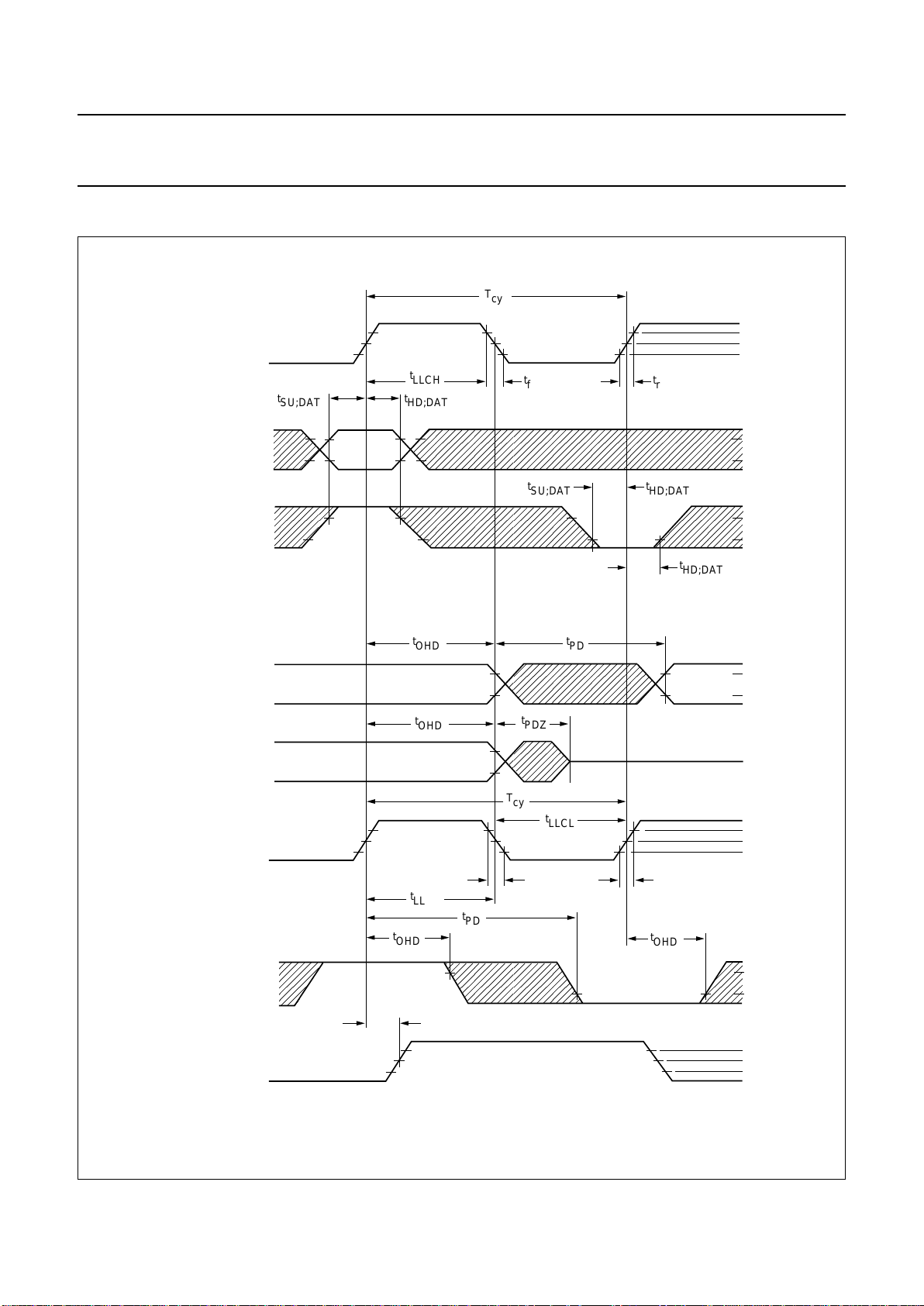
13 TIMING
14 OUTPUT FORMATS
15 CLOCK SYSTEM
15.1 Clock generation circuit
15.2 Power-on control
16 I2C-BUS DESCRIPTION
16.1 I2C-bus format
16.2 I2C-bus receiver/transmitter tables
16.3 I2C-bus detail
16.4 I2C-bus detail (continued)
17 SOURCE SELECTION MANAGEMENT
18 ANTI-ALIAS FILTER GRAPHS
19 CORING FUNCTION
19.1 Coring function adjustment by subaddress 06H
to affect band filter output adjustment
20 LUMINANCE FILTER GRAPHS
21 I2C-BUS START SET-UP
21.1 Remarks to Table 66
22 APPLICATION INFORMATION
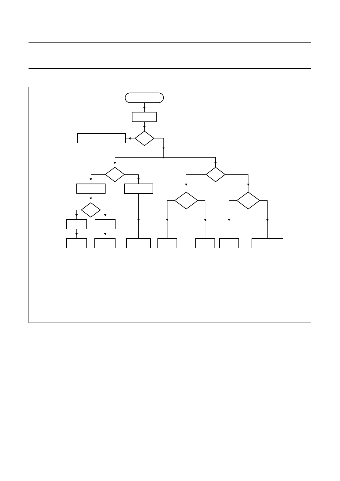
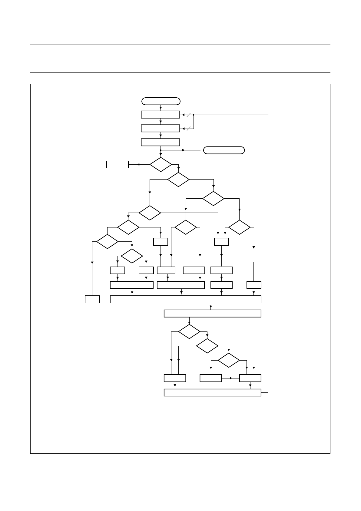
23 START-UP, SOURCE SELECT AND
STANDARD DETECTION FLOW EXAMPLE
23.1 CODE 0 STARTUP and STANDARD
Procedure
23.2 MODE 0 Source Select Procedure
23.3 MODE 1 Source Select Procedure
23.4 MODE 2 Source Select Procedure
23.5 MODE 3 Source Select Procedure
23.6 MODE 4 Source Select Procedure
23.7 MODE 5 Source Select Procedure
23.8 MODE 6 Source Select Procedure
23.9 MODE 7 Source Select Procedure
23.10 MODE 8 Source Select Procedure
24 PACKAGE OUTLINE
25 SOLDERING
25.1 Introduction
25.2 Reflow soldering
25.3 Wave soldering
25.4 Repairing soldered joints
26 DEFINITIONS
27 LIFE SUPPORT APPLICATIONS
28 PURCHASE OF PHILIPS I2C COMPONENTS

1995 Oct 18 3
Philips Semiconductors Product specification
One Chip Front-end 1 (OCF1) SAA7110; SAA7110A
1 FEATURES
• Six analog inputs (6 × CVBS or 3 × Y/C or
combinations)
• Three analog processing channels
• Three built-in analog anti-aliasing filters
• Analog signal adding of two channels
• Two 8-bit video CMOS analog-to-digital converters
• Fully programmable static gain for the main channels or
automatic gain control for the selected CVBS/Y channel
• Selectable white peak control signal
• Luminance and chrominance signal processing for
PAL B/G, NTSC M and SECAM
• Full range HUE control
• Automatic detection of 50/60 Hz field frequency, and
automatic switching between standards PAL and NTSC,
SECAM forceable
• Horizontal and vertical sync detection for all standards
• Cross-colour reduction by chrominance comb filtering
for NTSC or special cross-colour cancellation for
SECAM
• UV signal delay lines for PAL to correct chrominance
phase errors
• The YUV-bus supports a data rate of:
– 780 × f
h
= 12.2727 MHz for 60 Hz (NTSC)
– 944 × fh= 14.75 MHz for 50 Hz (PAL/SECAM)
• Square pixel format with 768/640 active samples per
line on the YUV-bus
• CCIR 601 level compatible
• 4:2:2 and 4:1:1 YUV output formats in 8-bit
resolution
• User programmable luminance peaking for aperture
correction
• Compatible with memory-based features
(line-locked clock, square pixel)
• Requires only one crystal (26.8 MHz) for all standards
• Real time status information output (RTCO)
• Brightness Contrast Saturation (BCS) control for the
YUV-bus
• Negation of picture possible
• One user programmable general purpose switch on an
output pin
• Switchable between on-chip Clock Generation Circuit
(CGC) and external CGC (SAA7197)
• Power-on control
• I
2
C-bus controlled.
2 APPLICATIONS
• Desktop video
• Multimedia
• Digital television
• Image processing
• Video phone
• Video picture grabbing.
3 GENERAL DESCRIPTION
The one chip front-end SAA7110; SAA7110A is a digital
multistandard colour decoder (OCF1) on the basis of the
DIG-TV2 system with two integrated Analog-to-Digital
Converters (ADCs), a Clock Generation Circuit (CGC) and
Brightness Contrast Saturation (BCS) control.
The CMOS circuit SAA7110; SAA7110A, analog front-end
and digital video decoder, is a highly integrated circuit for
desktop video applications. The decoder is based on the
principle of line-locked clock decoding. It operates
square-pixel frequencies to achieve correct aspect ratio.
Monitor controls are provided to ensure best display. The
circuit is I
2
C-bus controlled.
4 QUICK REFERENCE DATA
SYMBOL PARAMETER MIN. MAX. UNIT
V
DDA
analog supply voltage 4.75 5.25 V
V
DDD
digital supply voltage 4.5 5.5 V
T
amb
operating ambient temperature 0 70 °C
1995 Oct 18 4
Philips Semiconductors Product specification
One Chip Front-end 1 (OCF1) SAA7110; SAA7110A
5 ORDERING INFORMATION
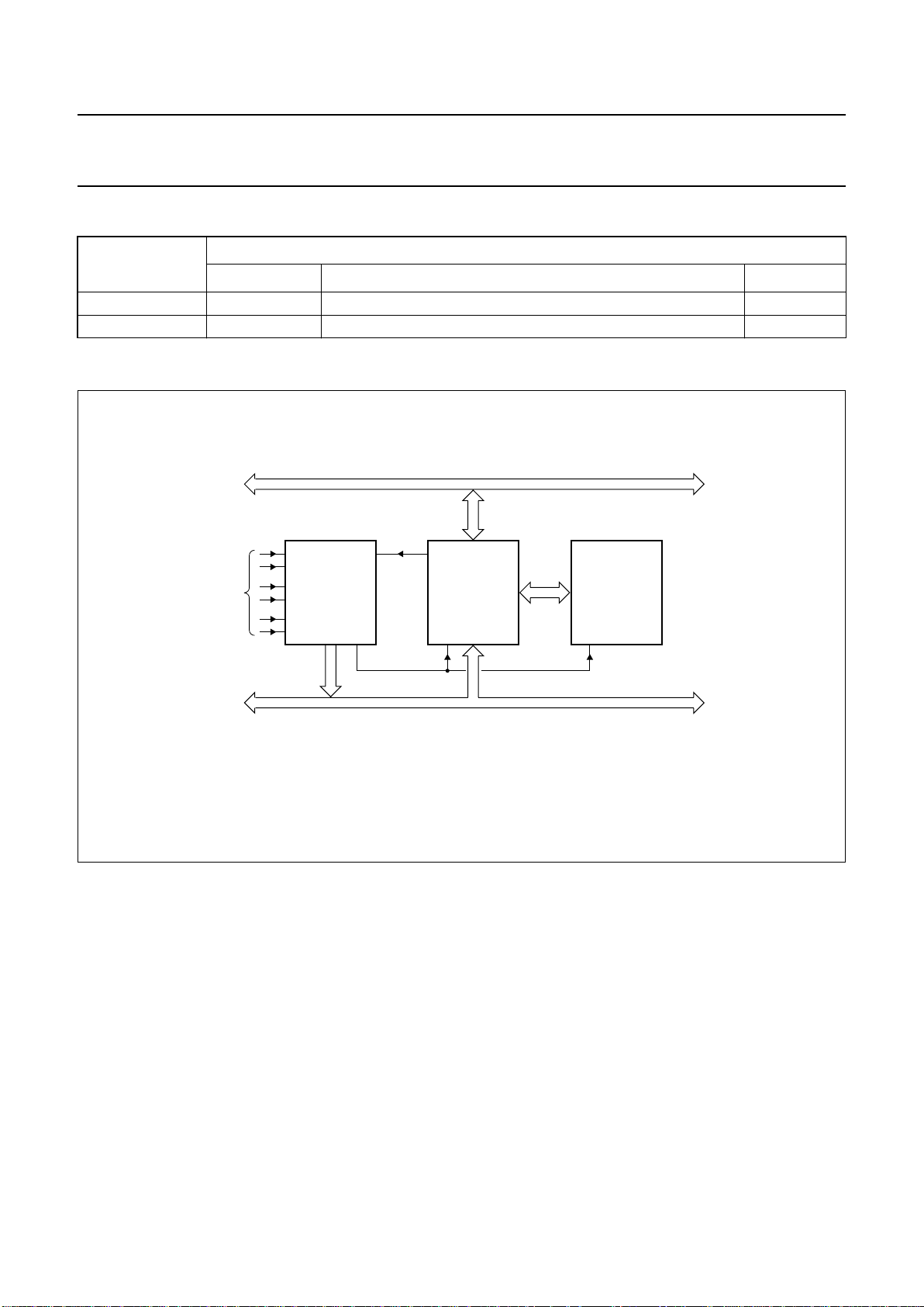
6 SYSTEM VIEW
TYPE NUMBER
PACKAGE
NAME DESCRIPTION VERSION
SAA7110 PLCC68 plastic leaded chip carrier; 68 leads SOT188-2
SAA7110A PLCC68 plastic leaded chip carrier; 68 leads SOT188-2
Fig.1 System diagram.
handbook, full pagewidth
VIDEO
MEMORY
CONTROLLER
VMC
ONE
CHIP
FRONT-END
OCF1
VIDEO
FRAME
MEMORY
six
video inputs
PC ISA - BUS
YUV - BUS
I
2
C
clock
MGC821
1995 Oct 18 5
Philips Semiconductors Product specification
One Chip Front-end 1 (OCF1) SAA7110; SAA7110A
This text is here in white to force landscape pages to be rotated correctly when browsing through the pdf in the Acrobat reader.This text is here in
_white to force landscape pages to be rotated correctly when browsing through the pdf in the Acrobat reader.This text is here inThis text is here in
white to force landscape pages to be rotated correctly when browsing through the pdf in the Acrobat reader. white to force landscape pages to be ...
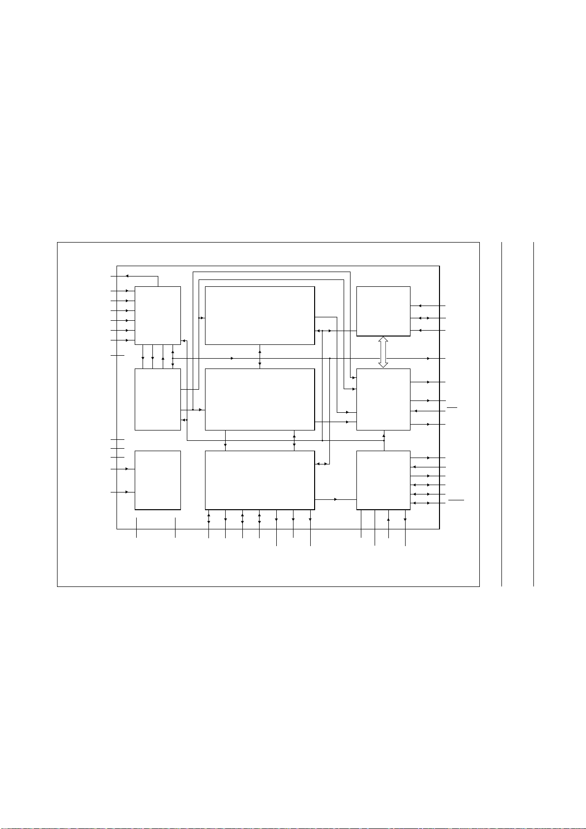
7 BLOCK DIAGRAM
handbook, full pagewidth
FEIN
(MUXC)
XTALO
XTALI
RESET
Y7 to Y0
SCL
SDA
SA
GPSW
(VBLK)
AP
SP
HS
RTCO
HSY HCLVS
SAA7110
SAA7110A
Y
Y
AD2 AD3
ANALOG
CONTROL
TEST
CONTROL
BLOCK
ANALOG
PROCESSING
CON
BYPASS
41 38
37
36
30
66
65
42
63
64
8
6
5
4
31
29
32
LLC2
CREF
UV7
to
UV0
i.c.
7, 8, 9
AI42
AI41
AI32
AI31
AI22
AI21
11
13
15
17
19
21
39
MGC820
40
ODD (VL)
PLIN (HL)
CGCE
LFCO
LLC
V
SSA0
V
DDA0
2524
68, 52, 44,
34, 27
67, 51, 43,
35, 28
V
SSA2
to V
SSA4
V
DDA2
to V
DDA4
V
SS
V
DD
V
SS(S)
18, 14, 10
20, 16, 12
22
Y/CVBS
C/CVBS
1
2
3 26
33
AOUT
23
HREF
CHROMINANCE
CIRCUIT
LUMINANCE
CIRCUIT
SYNCHRONIZATION
CIRCUIT
CLOCK
GENERATION
CIRCUIT
BRIGHTNESS
CONTRAST
SATURATION
CONTROL
AND
OUTPUT
FORMATTER
POWER-ON
CONTROL
UV
Y
55 to 62
45 to 50,
53, 54
I
2
C-BUS
INTERFACE
I
2
C-BUS
CONTROL
CLOCKS
Fig.2 Block diagram.

1995 Oct 18 6
Philips Semiconductors Product specification
One Chip Front-end 1 (OCF1) SAA7110; SAA7110A
8 PINNING
SYMBOL PIN DESCRIPTION
SP 1 test pin input; (shift pin) connect to ground for normal operation
AP 2 test pin input; (action pin) connect to ground for normal operation
RTCO 3 Real Time Control Output. This pin is used to fit serially the increments of the HPLL and
FSC-PLL and information of the PAL or SECAM sequence.
SA 4 I
2
C-bus slave address select input. LOW: slave address = 9CH for write, 9DH for read;
HIGH = 9DH for write, 9FH for read.
SDA 5 I
2
C-bus serial data input/output
SCL 6 I
2
C-bus serial clock input
i.c. 7 reserved pin; do not connect
i.c. 8 reserved pin; do not connect
i.c. 9 reserved pin; do not connect
V
SSA4
10 ground for analog input 4
AI42 11 analog input 42
V
DDA4
12 supply voltage (+5 V) for analog input 4
AI41 13 analog input 41
V
SSA3
14 ground for analog input 3
AI32 15 analog input 32
V
DDA3
16 supply voltage (+5 V) for analog input 3
AI31 17 analog input 31
V
SSA2
18 ground for analog input 2
AI22 19 analog input 22
V
DDA2
20 supply voltage (+5 V) for analog input 2
AI21 21 analog input 21
V
SS(S)
22 substrate ground
AOUT 23 analog test output; do not connect
V
DDA0
24 supply voltage (+5 V) for internal CGC (Clock Generation Circuit)
V
SSA0
25 ground for internal CGC
LFCO 26 Line Frequency Control output; this is the analog clock control signal driving the external
CGC. The frequency is a multiple of the actual line frequency (nominally 7.375/6.13636 MHz).
The signal has a triangular form with 4-bit accuracy.
V
DD
27 supply voltage (+5 V)
V
SS
28 ground
LLC 29 Line-Locked Clock input/output (CGCE = 1, output; CGCE = 0, input). This is the system
clock, its frequency is 1888 × f
h
for 50 Hz/625 lines per field systems and 1560 × fh for
60 Hz/525 lines per field systems; or variable input clock up to 32 MHz in input mode.
LLC2 30 Line-Locked Clock
1
⁄2output; f
LLC2
= 0.5 × f
LLC
(CGCE = 1, output; CGCE = 0, high
impedance).
CREF 31 Clock reference input/output (CGCE = 1, output; CGCE = 0, input). This is a clock qualifier
signal distributed by the internal or an external clock generator circuit (CGC). Using CREF all
interfaces on the YUV-bus are able to generate a bus timing with identical phase.
1995 Oct 18 7
Philips Semiconductors Product specification
One Chip Front-end 1 (OCF1) SAA7110; SAA7110A
RESET 32 Reset active LOW input/output (CGCE = 1, output; CGCE = 0, input); sets the device into a
defined state. All data outputs are in high impedance state. The I2C-bus is reset (waiting for
START condition). Using the external CGC, the LOW period must be maintained for at least
30 LLC clock cycles.
CGCE 33 CGC Enable active HIGH input (CGCE = 1, on-chip CGC active; CGCE = 0, external CGC
mode, use SAA7197).
V
DD
34 supply voltage (+5 V)
V
SS
35 ground
HCL 36 Horizontal Clamping input/output pulse (programmable via I
2
C-bus bit PULIO: PULIO = 1,
output; PULIO = 0, input). This signal is used to indicate the black level clamping period for
the analog input interface. The beginning and end of its HIGH period (only in the output mode)
can be programmed via the I2C-bus registers 03H, 04H in 50 Hz mode and registers 16H,
17H in 60 Hz mode, active HIGH.
HSY 37 Horizontal Synchronization input/output indicator (programmable via I
2
C-bus bit PULIO:
PULIO = 1, output; PULIO = 0, input). This signal is fed to the analog interface. The beginning
and end of its HIGH period (only in the output mode) can be programmed via the I2C-bus
registers 01H, 02H in 50 Hz mode and registers 14H, 15H in 60 Hz mode, active HIGH.
HS 38 Horizontal Synchronization output (programmable; the HIGH period is 128 LLC clock cycles).
The position of the positive slope is programmable in 8 LLC increments over a complete line
(64 µs) via the I
2
C-bus register 05H in 50 Hz mode or register 18H in 60 Hz mode.
PLIN (HL) 39 PAL Identifier Not output; marks for demodulated PAL signals the inverted line (PLIN = LOW)
and a non-inverted line (PLIN = HIGH) and for demodulated SECAM the DR line
(PLIN = LOW) and the DB line (PLIN = HIGH). Select PLIN function via I
2
C-bus bit RTSE = 0.
(H-PLL locked output; a HIGH state indicates that the internal PLL has locked. Select HL
function via I2C-bus bit RTSE = 1).
ODD (VL) 40 ODD/EVEN field identification output; a HIGH state indicates the odd field. Select ODD
function via I
2
C-bus bit RTSE = 0.
(Vertical Locked output; a HIGH state indicates that the internal Vertical Noise Limiter (VNL)
is in a locked state. Select VL function via I2C-bus bit RTSE = 1).
VS 41 Vertical Synchronization input/output (programmable via I
2
C-bus bit OEHV: OEHV = 1,
output; OEHV = 0, input). This signal indicates the vertical synchronization with respect to the
YUV output. The high period of this signal is approximately six lines if the VNL function is
active. The positive slope contains the phase information for a deflection controller, for
example the TDA9150. In input mode this signal is used to synchronize the vertical gain and
clamp blanking stage, active HIGH.
HREF 42 Horizontal Reference output; this signal is used to indicate data on the digital YUV-bus. The
positive slope marks the beginning of a new active line. The HIGH period of HREF is either
768 Y samples or 640 Y samples long depending on the detected field frequency
(50/60 Hz mode). HREF is used to synchronize data multiplexer/demultiplexers. HREF is also
present during the vertical blanking interval.
V
SS
43 ground
V
DD
44 supply voltage (+5 V)
SYMBOL PIN DESCRIPTION

1995 Oct 18 8
Philips Semiconductors Product specification
One Chip Front-end 1 (OCF1) SAA7110; SAA7110A
Y7 45
Upper 6 bits of the 8-bit luminance (Y) digital output. As part of the digital YUV-bus
(data rate LLC/2), or A/D2(3) output (data rate LLC/2) selectable via I
2
C-bus bit SQPB = 1.
Y6 46
Y5 47
Y4 48
Y3 49
Y2 50
V
SS
51 ground
V
DD
52 supply voltage (+5 V)
Y1 53
Lower 2 bits of the 8-bit luminance (Y) digital output. As part of the digital YUV-bus
(data rate LLC/2), or A/D2(3) output (data rate LLC/2) selectable via I
2
C-bus bit SQPB = 1.
Y0 54
UV7 55
8-bit digital UV (colour difference) output; multiplexed colour difference signal for U and V
component of demodulated CVBS or chrominance signal. The format and multiplexing
scheme can be selected via I
2
C-bus control. These signals are part of the digital YUV-bus
(data rate LLC/2), or A/D3(2) output (data rate LLC/2) selectable via I2C-bus bit SQPB = 1.
UV6 56
UV5 57
UV4 58
UV3 59
UV2 60
UV1 61
UV0 62
FEIN
(MUXC)
63 Fast Enable input (active LOW); this signal is used to control fast switching on the digital
YUV-bus. A high at this input forces the IC to set its Y and UV outputs to the high impedance
state. To use this function set I2C-bus bits MS24 and MS34 and MUYC to LOW.
(Multiplex Components input; control signal for the analog multiplexers for fast switching
between locked Y/C signals or locked CVBS signals. FEIN automatically fixed to LOW (digital
YUV-bus enabled), if one of the three MUXC functions are selected (MS24 or MS34 or
MUYC = HIGH).
GPSW
(VBLK)
64 General Purpose Switch output; the state of this signal is programmable via I
2
C-bus register
0Dh, bit 1. Select GPSW function via I2C-bus bit VBLKA = 0. (Vertical Blank test output; select
VBLK via I2C-bus bit VBLKA = 1).
XTALO 65 Crystal oscillator output (to 26.8 MHz crystal); not used if TTL clock is used.
XTALI 66 Crystal oscillator input (from 26.8 MHz crystal) or connection of external oscillator with TTL
compatible square wave clock signal.
V
SS
67 ground
V
DD
68 supply voltage (+5 V)
SYMBOL PIN DESCRIPTION
1995 Oct 18 9
Philips Semiconductors Product specification
One Chip Front-end 1 (OCF1) SAA7110; SAA7110A
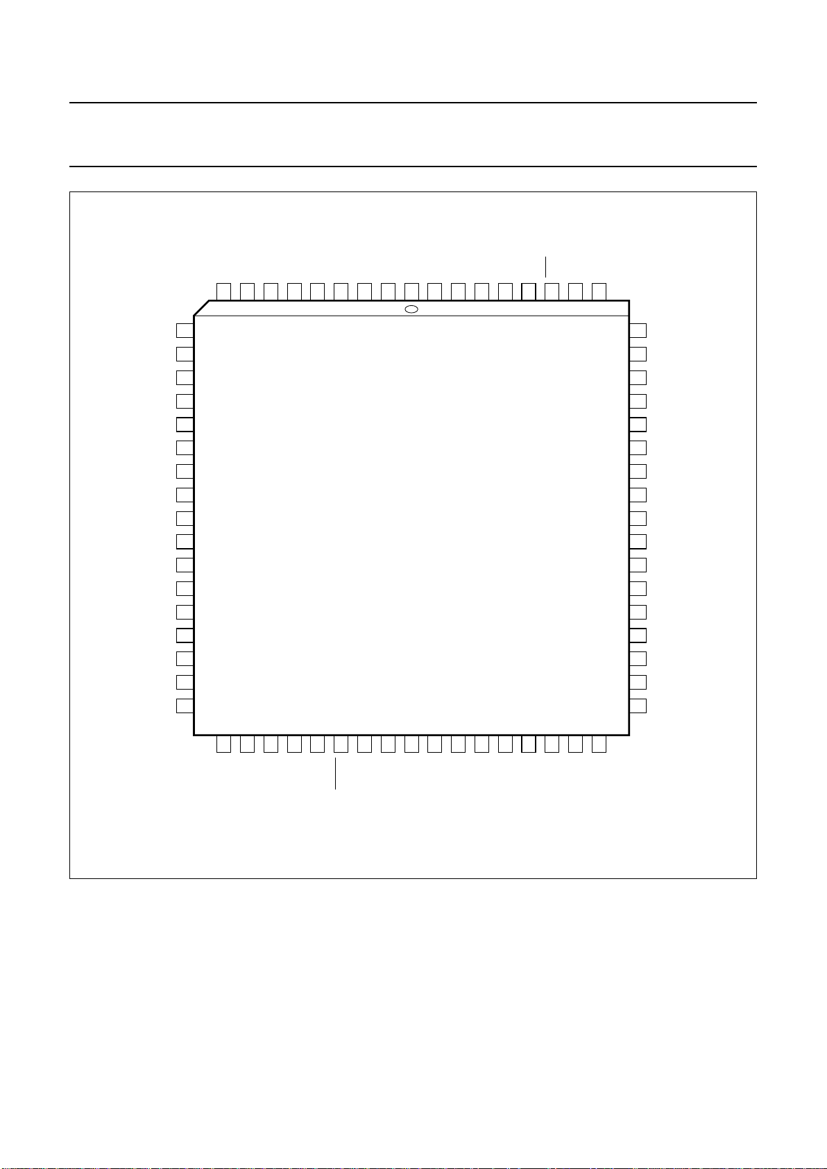
Fig.3 Pin configuration.
handbook, full pagewidth
SAA7110
SAA7110A
MGC822
10
11
12
13
14
15
16
17
18
19
20
21
22
23
24
25
26
60
59
58
57
56
55
54
53
52
51
50
49
48
47
46
45
Y7
Y6
Y5
Y4
Y3
Y2
Y1
Y0
UV7
UV6
UV5
UV4
UV3
UV2
44
27
28
29LLC
LLC2
CREF
RESET
CGCE
HS
VS
PLIN (HL)
ODD (VL)
HREF
HCL
HSY
30
31
32
33
34
35
36
37
38
39
40
41
42
43
9
8
7
6
5
4
3
2
1
68
67
66 XTALI
XTALO
SP
AP
RTCO
SA
i.c.
i.c.
i.c.
SDA
SCL
GPSW (VBLK)
FEIN (MUXC)
UV0
UV1
65
64
63
62
61
V
SSA4
AI42
V
DDA4
AI41
AI32
AI31
AI22
AI21
AOUT
V
SSA3
VDDV
SS
V
DDA3
V
SSA2
V
DDA2
V
SS(S)
V
DDA0
V
DD
V
SS
V
DD
V
SS
V
SS
V
DD
V
SS
V
DD
V
SSA0
LFCO
1995 Oct 18 10
Philips Semiconductors Product specification
One Chip Front-end 1 (OCF1) SAA7110; SAA7110A
9 FUNCTIONAL DESCRIPTION
9.1 Analog input processing (see Fig.5)
The SAA7110; SAA7110A offers six analog signal inputs,
two analog main channels with clamping circuit, analog
amplifier, anti-alias filter and video CMOS ADC. A third
analog channel also with clamping circuit, analog amplifier
and anti-alias filter can be added or switched to both main
channels directly before the ADCs.
9.2 Analog control circuits
The clamping control circuit controls the correct clamping
of the analog input signals. The coupling capacitor is also
used to store and filter the clamping voltage. The normal
digital clamping level for luminance or CVBS signals is 64
and for chrominance signals is128.
The gain control circuits generate via I
2
C-bus the static
gain levels for the three analog amplifiers or controls one
of these amplifiers automatically via a built-in Automatic
Gain Control (AGC). The AGC is used to amplify a
CVBS or Y signal to the required signal amplitude,
matched to the ADCs input voltage range.
The anti-alias filters are adapted to the clock frequency.
The vertical blanking control circuit generates an I2C-bus
programmable vertical blanking pulse. During the vertical
blanking time gain and clamping control are frozen.
The fast switch control circuit is used for special
applications.
9.2.1 C
LAMPING
The coupling capacitor is used as clamp capacitance for
each input. An internal digital clamp comparator generates
the information concerning clamp-up or clamp-down. The
clamping levels for the two ADC channels are adjustable
over the 8-bit range (1 to 254). Clamping time in normal
use is set with the HCL pulse at the back porch of the video
signal. The clamping pulse HCL is user adjustable.
9.2.2 G
AIN CONTROL (see Fig.4)
The luminance AGC can be used for every channel were
luminance or CVBS is being received. AGC active time is
the sync tip of the video signal. The sync tip pulse HSY is
user adjustable. The AGC can be switched off and the gain
for the three main input channels can be adjusted
independently. Signal (white) peak control limits the gain
at signal overshoots. The flow charts (see Figs 8 and 9)
show more details of the AGC. The influence of supply
voltage variation within the specified range is automatically
eliminated by clamp and automatic gain control.
9.3 Chrominance processing (see Fig.6)
The 8-bit chrominance signal passes the input interface,
the chrominance bandpass filter to eliminate DC
components, and is finally fed to the multiplication inputs
of a quadrature demodulator, where two subcarrier signals
from the local oscillator DTO1 with 90 degrees phase shift
are applied. The frequency is dependent on the present
colour standard.
The multiplier operates as a quadrature demodulator for all
PAL and NTSC signals; it operates as a frequency down
mixer for SECAM signals.
The two multiplier output signals are converted to a serial
UV data stream and applied to two low-pass filter stages,
then to a gain controlled amplifier. A final multiplexed
low-pass filter achieves, together with the preceding
stages, the required bandwidth performance.
The PAL and NTSC originated signals are applied to a
comb filter.
The signal originated from SECAM is fed through a Cloche
filter (0 Hz centre frequency), a phase demodulator and a
differentiator to obtain frequency demodulated colour
difference signals. The SECAM signal is fed after
de-emphasis to a cross-over switch, to provide both the
serial transmitted colour difference signals. These signals
are fed to the BCS control and finally to the output fomatter
stage and to the output interface.
Fig.4 Automatic gain control range.
handbook, halfpage
analog input level
controlled
ADC input level
maximum
minimum
range 8.8 dB
0 dB
0 dB
MGC823
+2.8 dB
−6 dB

1995 Oct 18 11
Philips Semiconductors Product specification
One Chip Front-end 1 (OCF1) SAA7110; SAA7110A
9.4 Luminance processing (see Fig.7)
The 8-bit luminance signal, a digital CVBS format or a
luminance format (S-VHS, HI8), is fed through a
switchable prefilter. High frequency components are
emphasized to compensate for loss. The following
chrominance trap filter (fc= 4.43 or 3.58 MHz centre
frequency selectable) eliminates most of the colour carrier
signal, therefore, it must be bypassed for S-Video (S-VHS,
HI8) signals.
The high frequency components of the luminance signal
can be peaked (control for sharpness improvement via
I
2
C-bus) in two bandpass filters with selectable transfer
characteristics.
A coring circuit with selectable characteristics improves
the signal once more. This signal is then added to the
original (unpeaked) signal. A switchable amplifier achieves
common DC amplification, because the DC gains are
different in both chrominance trap modes.
The improved luminance signal is fed via the variable
delay to the BCS control and the output interface.
9.5 YUV-bus (digital outputs)
The 16-bit YUV-bus transfers digital data from the output
interfaces to a feature box, or a field memory, a digital
colour space converter (SAA 7192 DCSC) or a video
enhancement and digital-to-analog processor (SAA7165
VEDA2). The outputs are controlled by an output enable
chain (
FEIN on pin 63).
The YUV data rate equals LLC2. Timing is achieved by
marking each second positive rising edge of the clock LLC
in conjunction with CREF (clock reference).
The output signals Y7 to Y0 are the bits of the digital
luminance signal. The output signals UV7 to UV0 are the
bits of multiplexed colour difference signals (B−Y) and
(R−Y). The frame in the format tables is the time, required
to transfer a full set of samples. In the event of 4 :2:2
format two luminance samples are transmitted in
comparison to one U and one V sample within the frame.
The time frames are controlled by the HREF signal.
Fast enable is achieved by setting inputFEIN to LOW. The
signal is used to control fast switching on the digital
YUV-bus. HIGH on this pin forces the Y and UV outputs to
a high-impedance state.
9.6 Synchronization (see Fig.7)
The pre-filtered luminance signal is fed to the
synchronization stage. It's bandwidth is reduced to 1 MHz
in a low-pass filter.
The synchronization pulses are sliced and fed to the phase
detectors where they are compared with the sub-divided
clock frequency. The resulting output signal is applied to
the loop filter to accumulate all phase deviations.
Adjustable output signals HCL and HSY are generated in
accordance with analog front end requirements. The
output signals HS, VS, and PLIN are locked to the timing
reference, guaranteed between the input signal and the
HREF signal, as further improvements to the circuit may
change the total processing delay. It is therefore not
recommended to use them for applications which require
absolute timing accuracy to the input signals. The loop
filter signal drives an oscillator to generate the line
frequency control signal LFCO.
9.7 Clock generation circuit
The internal CGC generates all clock signals required for
the one chip front-end. The output signal LFCO is a
digital-to-analog converted signal provided by the
horizontal PLL. It is the multiple of the line frequency
(7.38 MHz = 472 × f
h
in 50 Hz systems and
6.14 MHz = 360 × fh in 60 Hz systems). Internally the
LFCO signal is multiplied by a factor of 2 or 4 in the PLL
circuit (including phase detector, loop filtering, VCO and
frequency divider) to obtain the LLC and LLC2 output clock
signals. The rectangular output clocks have a 50% duty
factor.
It is also possible to operate the OCF1 with an external
CGC (SAA7197) providing the signals LLC and CREF.
The selection of the internal/external CGC will be
controlled by the CGCE input signal.
9.8 Power-on reset
Power-on reset is activated at power-on (using only
internal CGC), when the supply voltage decreases below
3.5 V. The indicator output
RESET is LOW for a time. The
RESET signal can be applied to reset other circuits of the
digital TV system.
9.9 RTCO output
The real time control and status output signal contains
serial information about actual system clock, subcarrier
frequency and PAL/SECAM sequence. The signal can be
used for various applications in external circuits, for
example, in a digital encoder to achieve clean encoding.
1995 Oct 18 12
Philips Semiconductors Product specification
One Chip Front-end 1 (OCF1) SAA7110; SAA7110A
This text is here in white to force landscape pages to be rotated correctly when browsing through the pdf in the Acrobat reader.This text is here in
_white to force landscape pages to be rotated correctly when browsing through the pdf in the Acrobat reader.This text is here inThis text is here in
white to force landscape pages to be rotated correctly when browsing through the pdf in the Acrobat reader. white to force landscape pages to be ...
handbook, full pagewidth
ANALOG
CONTROL
MGC824
SOURCE
SWITCH
CLAMP
CIRCUIT
ANALOG
AMPLIFIER
ANALOG
AMPLIFIER
ANALOG
AMPLIFIER
GAIN
CONTROL
CLAMP
CONTROL
CROSS
MULTIPLEXER
ANTI-ALIAS
FILTER
BYPASS
SWITCH
SOURCE
SWITCH
CLAMP
CIRCUIT
ANTI-ALIAS
FILTER
BYPASS
SWITCH
FAST
SWITCH
ADDER
FAST
SWITCH
ADDER
FAST
SWITCH
CONTROL
VERTICAL
BLANKING
CONTROL
SOURCE
SWITCH
CLAMP
CIRCUIT
ANTI-ALIAS
FILTER
ANTI-ALIAS
CONTROL
BYPASS
SWITCH
TEST
SELECTOR
FUSE
FUSE
FUSE
REFS4AINS4
AIND4
REFS3
REFS2
AINS3
AIND3
AINS2
AIND2
CLTS
CLS2
CLS3
CLS4
AOSL
ADC
ADC
YSEL
CSEL
TWO2
TWO3
V
DDA2
to V
DDA4
V
SSA2
to V
SSA4
AI42
AI41
AI32
AI31
AI22
AI21
i.c.
i.c.
i.c.
V
SS(S)
11
20, 16, 12
18, 14, 10
13
15
17
19
21
9
8
7
22
CLL2n
CLL3n
WIPA
GLIM
HOLD
WIPE
SBOT
GASL
GACO
GAI2
GAI3
GAI4
IWIP
IGAI
VBPS
VBPR
VBCO
MUYC
MS24
MS34
MX24
MX34
MUD1
MUD2
WISL
IVAL
WVAL
GUDL
WIRS
GAS2
GAS3
GAD2
GAD3
WRSE
23
AOUT
Fig.5 Analog input processing and analog control part.
1995 Oct 18 13
Philips Semiconductors Product specification
One Chip Front-end 1 (OCF1) SAA7110; SAA7110A
This text is here in white to force landscape pages to be rotated correctly when browsing through the pdf in the Acrobat reader.This text is here in
_white to force landscape pages to be rotated correctly when browsing through the pdf in the Acrobat reader.This text is here inThis text is here in
white to force landscape pages to be rotated correctly when browsing through the pdf in the Acrobat reader. white to force landscape pages to be ...
handbook, full pagewidth
INPUT
INTERFACE
CHROMINANCE
BANDPASS
OUTPUT
FORMATTER
AND INTERFACE
QUADRATURE
DEMODULATOR
LOW-PASS LOW-PASS
GAIN
CONTROL
CLOCH FILTER
LOOPFILTER
PI2
LOOP FILTER
PI1
SEQUENCE
PROCESSOR
PHASE
DEMODULATOR
AMPLITUDE
DETECTOR
BRIGHTNESS
CONTRAST
SATURATION
CONTROL
COMB FILTERS
AND SECAM
RECOMBINATION
BURST GATE
ACCUMULATOR
DISCRETE TIME
OSCILLATOR
(DTO1)
AND DIVIDER
STANDARD
CONTROL
BRIG
CONT
SATN
DIFFERENTIATOR
DE-EMPHASIS
SXCRCODE
BYPS
CHRS
COLO
SECS
CHCV
CKTQ
CKTS
LFIS
SEQA
SESE
PLSE
ALTD
V
DD
V
SS
CHROMINANCE CIRCUIT
68, 52, 44,
34, 27
67, 51, 43,
35, 28
63
42
OFTS
CHSB
OEYC
OEHV
SQPB
HRMV
HRFS
SEQA
HUEC
FEIN
(MUXC)
HREF
UV7 to UV0
Y7 to Y0
45 to 50,
53, 54
MGC825
55 to
62
Fig.6 Multi-standard decoder part.
1995 Oct 18 14
Philips Semiconductors Product specification
One Chip Front-end 1 (OCF1) SAA7110; SAA7110A
This text is here in white to force landscape pages to be rotated correctly when browsing through the pdf in the Acrobat reader.This text is here in
_white to force landscape pages to be rotated correctly when browsing through the pdf in the Acrobat reader.This text is here inThis text is here in
white to force landscape pages to be rotated correctly when browsing through the pdf in the Acrobat reader. white to force landscape pages to be ...
handbook, full pagewidth
PREFILTER
PREFILTER
SYNC
I2C-BUS
INTERFACE
I
2
C-BUS
CONTROL
SYNC
SLICER
TEST
CONTROL
BLOCK
CHROMINANCE
TRAP
PHASE
DETECTOR
FINE
PHASE
DETECTOR
COARSE
LOOP FILTER
2
DELAY
ADJUSTMENT
LINE-LOCKED
CLOCK
GENERATOR
DISCRETE TIME
OSCILLATOR
(DTO2)
CRYSTAL
CLOCK
GENERATOR
VARIABLE
BANDPASS
FILTER
CORING
WEIGHTING
AND
ADDING STAGE
VARIABLE
DELAY
POWER-ON
CONTROL
PREF BYPS CORI APER YDEL
CLOCK(3 to 0)
BFBY
PREF
BPSS
MATCHING
AMPLIFIER
DAC6
CLOCK
GENERATION
CIRCUIT
DAC4
COUNTER
VERTICAL
PROCESSOR
FIDT
HLCK
STTC
VBLKA
SSTB
GPSW
VNOI
FSEI
AUFD
HS6B
HS6S
HC6B
HC6S
PULIO
OEHV
SCEN
IDEL
HSYB
HSYS
HCLB
HCLS
HPHI
HP6I
SYNCHRONIZATION CIRCUIT
LUMINANCE CIRCUIT
HLCK
VTRC
HPLL
HLCK
AP
SP
SA SCL SDA
36
64
456
4137 38 39 40 25 24 333
HCL HS VS
CGCEODD (VL)
V
SSA0
V
DDA0
RTCO
HSY
PLIN (HL)
26
65
66
30
29
31
32
RESET
CREF
LLC
LLC2
XTALI
XTALO
LFCO
GPSW
(VBLK)
2
1
MGC826
Fig.7 Luminance and synchronization part.
1995 Oct 18 15
Philips Semiconductors Product specification
One Chip Front-end 1 (OCF1) SAA7110; SAA7110A
10 GAIN CHARTS
Fig.8 Clamp and gain flow chart.
CLAU = clamp up.
VBLK = vertical blanking pulse.
WIPE = white peak level (adjustable).
SBOT = sync bottom level (adjustable).
CLL = clamp level (adjustable).
CLAA = clamp active.
HSY = horizontal sync pulse.
HCL = horizontal clamp pulse.
handbook, full pagewidth
ADC
ANALOG IN
VBLK
NO BLANKING ACTIVE
CLAA = 1
HCL
<
CCL
HSY
>
SBOT
> WIPE
CLAA = 0
CLAU = 1 CLAU = 0
10 10
MGC827
+ CLAMP − CLAMP + GAIN − GAIN − GAIN SLOW + GAINNO CLAMP
10
10
10
10
<− CLAMP GAIN −>
1995 Oct 18 16
Philips Semiconductors Product specification
One Chip Front-end 1 (OCF1) SAA7110; SAA7110A
handbook, full pagewidth
analog input
amplifier
anti-alias amplifier
ADC8
decoder input
X
HSY
WRSE
>WIPE
>WIPE
<SBOT<SBOT
WIRS
X = 1X = 0
−
IVAL
+IVAL −WVAL
+/− 0
+4/F
+4/L
gain accumulator (20 bits)
actual gain value 8-bit (AGV) [−3/+6 dB]
X
STOP
HSY
Y
update
FGV
MGC828
AGV
gain value 8-bit
1
0
1
0
1
0
1
0
1
0
1
0
1
0
0
1
1
0
1
0
1
0
VBLK
1
0
no action
MSB
6
LSB
2
*IWIP *IGAI *IWIP
Fig.9 Luminance AGC flow chart.
X = system variable (start with logic 0).
Y = IAGV-FGVI > GUDL.
VBLK = vertical blanking pulse.
HSY = horizontal sync pulse.
SBOT = sync bottom level (adjustable).
WIPE = white peak level (adjustable).
IVAL = integration value gain (adjustable).
WVAL = integration value WIPE (adjustable).
IGAI = integration factor gain (adjustable).
IWIP = integration factor WIPE (adjustable).
AGV = actual gain value.
FGV = frozen gain value.
GUDL = gain update level (adjustable).
WRSE = white peak reset enable.
WIRS = white peak reset select.
L = line.
F = field.

1995 Oct 18 17
Philips Semiconductors Product specification
One Chip Front-end 1 (OCF1) SAA7110; SAA7110A
11 LIMITING VALUES
In accordance with the Absolute Maximum Rating System (IEC 134); all ground pins and all supply pins connected
together.
Note
1. Compare with typical total power consumption in Chapter “Characteristics”.
2. Equivalent to discharging a 100 pF capacitor through a 1.5 kΩ series resistor.
12 CHARACTERISTICS
V
DDD
=5V; V
DDA
=5V; T
amb
=25°C; unless otherwise specified.
SYMBOL PARAMETER CONDITIONS MIN. MAX. UNIT
V
DDA
analog supply voltage −0.5 +7.0 V
V
DDD
digital supply voltage −0.5 +7.0 V
V
I(A)
analog input voltage −0.5 +7.0 V
V
I(D)
digital input voltage −0.5 +7.0 V
V
diff
voltage difference between V
SSAall
and V
SSall
− 100 mV
T
stg
storage temperature −65 +150 °C
T
amb
operating ambient temperature 0 70 °C
T
amb(bias)
operating ambient temperature under bias −10 +80 °C
P
tot
total power dissipation V
DDA=VDDD
= 7 V; note 1 − 2.5 W
V
esd
electrostatic discharge all pins note 2 −2000 +2000 V
SYMBOL PARAMETER CONDITIONS MIN. TYP. MAX. UNIT
Supplies
V
DDA
analog supply voltage 4.75 5.0 5.25 V
V
DDD
digital supply voltage 4.5 5.0 5.5 V
I
DDA(tot)
total analog supply current −−150 mA
I
DDD(tot)
total digital supply current −−250 mA
P
tot
total power dissipation − 1.2 1.7 W
Analog part
I
clamp
clamping current VI= 1.25 V DC −2 − +2 µA
V
i(p-p)
input voltage (peak-to-peak
value), AC coupling required
C
couple
= 10 nF 0.5 1.0 1.38 V
Z
i
input impedance clamping current off 200 −− kΩ
C
i
input capacitance −−10 pF
α
ct
channel crosstalk fi< 5 MHz −−50 − dB
Analog-to-digital converters
B analog bandwidth at −3dB − 15 − MHz
φ
diff
differential phase amplifier + AAF = bypass − 2 − deg
G
diff
differential gain amplifier + AAF = bypass − 2 − %
f
LLC
ADC clock rate 11 − 16 MHz
DLE DC differential linearity error −
1
⁄
2
− LSB
ILE DC integral linearity error − 1 − LSB

1995 Oct 18 18
Philips Semiconductors Product specification
One Chip Front-end 1 (OCF1) SAA7110; SAA7110A
Digital inputs
V
IL
LOW level input voltage
SDA and SCL
−0.5 − +1.5 V
V
IH
HIGH level input voltage
SDA and SCL
3.0 − VDD+ 0.5 V
V
IL(clk)
LOW level input voltage for
clocks
−0.5 − +0.6 V
V
IH(clk)
HIGH level input voltage for
clocks
2.4 − VDD+ 0.5 V
V
IH(XTALI)
HIGH level input voltage XTALI 3.0 − VDD+ 0.5 V
V
IL(n)
LOW level input voltage all other
inputs
−0.5 − +0.8 V
V
IH(n)
HIGH level input voltage all other
inputs
2.0 − VDD+ 0.5 V
I
LI
input leakage current −−10 µA
C
i(clk)
input capacitance for clocks −−10 pF
C
i(I/O)
input capacitance I/Os at high impedance −−8pF
C
i(n)
input capacitance all other inputs −−8pF
Digital outputs
V
LFCO
LFCO output voltage
(peak-to-peak value)
note 1 1.4 − 2.6 V
V
OL
LOW level output voltage note 2 0 − 0.6 V
V
OH
HIGH level output voltage note 2 2.4 − V
DD
V
V
OL(clk)
LOW level output voltage for
clocks
−0.5 − +0.6 V
V
OH(clk)
HIGH level output voltage for
clocks
2.6 − VDD+ 0.5 V
Clock input timing (LLC)
T
cy
cycle time 31 − 45 ns
δ duty factor for t
LLCH/Tcy
40 − 60 %
t
r
rise time Vi= 0.6 to 2.4 V −−5ns
t
f
fall time Vi= 2.4 to 0.6 V −−5ns
Control and CREF input timing (note 3)
t
SU;DAT
input data set-up time 11 −− ns
t
HD;DAT
input data hold time 3 −− ns
t
HD;FEIN
input data hold time for FEIN 3 −− ns
t
HD;OTHER
input data hold time all other
inputs
note 3 6 −− ns
SYMBOL PARAMETER CONDITIONS MIN. TYP. MAX. UNIT
1995 Oct 18 19
Philips Semiconductors Product specification
One Chip Front-end 1 (OCF1) SAA7110; SAA7110A
Data and control output timing (note 4)
C
L(data)
output load capacitance
(data, HREF and VS)
15 − 50 pF
C
L(control)
output load capacitance (control) 7.5 − 25 pF
t
HD;DAT
output data hold time CL=15pF 13 −− ns
t
PD(data)
propagation delay from negative
edge of LLC (data, HREF and
VS)
CL=50pF −−29 ns
t
PD(control)
propagation delay from negative
edge of LLC (control)
CL=25pF −−29 ns
t
PD(Z))
propagation delay from negative
edge of LLC (to 3-state)
note 5 −−15 ns
Clock output timing (LLC and LLC2)
C
L(LLC)
output load capacitance 15 − 40 pF
T
cy
cycle time LLC 31.5 − 45 ns
LLC2 63 − 90 ns
δ duty factors for t
LLCH/tLLC
and
t
LLC2H/tLLC2
40 − 60 %
t
r
rise time 0.6 to 2.6 V −−5ns
t
f
fall time 2.6 to 0.6 V −−5ns
t
d
delay time LLC output to LLC2
output
Vi= 1.5 V;
C
LLC/LLC2
= 40 pF; note 6
−−8ns
Data qualifier output timing (CREF)
t
HD;CREF
output hold time CL=15pF 4 −− ns
t
PD;CREF
propagation delay from positive
edge of LLC
CL=40pF −−20 ns
Horizontal PLL
f
Hnom
nominal line frequency 50 Hz field − 15625 − Hz
60 Hz field − 15734 − Hz
∆fH/f
Hnom
permissible static deviation 50 Hz field −−5.6 %
60 Hz field −−6.7 %
Subcarrier PLL
f
Hnom
nominal subcarrier frequency PAL − 4433618 − Hz
NTSC − 3579545 − Hz
∆f
H/fHnom
lock-in range 400 −− Hz
SYMBOL PARAMETER CONDITIONS MIN. TYP. MAX. UNIT
1995 Oct 18 20
Philips Semiconductors Product specification
One Chip Front-end 1 (OCF1) SAA7110; SAA7110A
Notes
1. The LFCO output level must be measured with a load circuit of 10 kΩ in parallel with 15 pF.
2. The levels must be measured with load circuits, the loads depend on the type of output stage. Control outputs (except
HREF and VS); 1.2 kΩ at 3 V (TTL load); CL= 25 pF: data outputs (plus HREF and VS); 1.2 kΩ at 3 V (TTL load);
CL=50pF.
3. Other control input signals are CGCE, VS, SA, HCL and HSY.
4. Data output signals are YUV (15 to 0). Control output signals are HREF, VS, HS, HSY, HCL, RTCO, PLIN (HL),
ODD (VL) and GPSW0 (VBLK). The effects of rise and fall times are included in the calculation of t
HD;DAT
, tPD and
t
PDZ
. Timings and levels refer to drawings and conditions illustrated in Fig.10.
5. The minimum propagation delay from 3-state to data active related to falling edge of LLC is 0 ns.
6. LLC2 is not active while CGCE = 0.
7. Philips catalogue number 9922 520 30004.
Table 1 Processing delay
Crystal oscillator
f
n
nominal frequency 3rd harmonic − 26.8 − MHz
∆f/f
n
permissible frequency deviation −50 × 10−6− +50 × 10
−6
∆T/f
n
permissible frequency deviation
with temperature
−20 × 10−6− +20 × 10
−6
CRYSTAL SPECIFICATION (X1); note 7
T
amb
operating ambient temperature 0 − 70 °C
C
L
load capacitance 8 −− pF
R
s
series resonance resistance − 50 80 Ω
C1 motional capacitance − 1.1 ±20% − fF
C0 parallel capacitance − 3.5 ±20% − pF
FUNCTION
TYPICAL ANALOG DELAY
AI21 TO ADCIN (AOUT) (ns)
DIGITAL DELAY
ADCIN (AOUT) TO YUVOUT
(1/LLC)
(YDEL = 0; CAD2/3 = 1)
Without amplifier or anti-alias filter 10
248
With amplifier, without anti-alias filter 30
With amplifier plus anti-alias filter (50 Hz) 30 + 40
With amplifier plus anti-alias filter (60 Hz) 30 + 50
SYMBOL PARAMETER CONDITIONS MIN. TYP. MAX. UNIT
1995 Oct 18 21
Philips Semiconductors Product specification
One Chip Front-end 1 (OCF1) SAA7110; SAA7110A
13 TIMING
Fig.10 Clock/data timing.
handbook, full pagewidth
T
cy
T
cy
t
f
t
SU;DAT
t
r
t
LLCH
t
SU;DAT
t
HD;DAT
t
HD;DAT
t
HD;DAT
t
OHD
t
OHD
t
PD
t
PDZ
t
PD
t
OHD
t
OHD
t
LLCL
t
LLCH
t
f
t
dLLC2
t
r
CLOCK INPUT LLC
INPUTS CONTROL
INPUT CREF
OUTPUTS YUV, HREF, VS AND HS
OUTPUTS YUV (to 3-state)
CLOCK OUTPUT LLC
OUTPUT CREF
CLOCK OUTPUT LLC2
2.4 V
1.5 V
0.6 V
2.6 V
1.5 V
0.6 V
2.6 V
1.5 V
0.6 V
2.0 V
0.8 V
2.0 V
0.8 V
2.4 V
0.6 V
2.4 V
0.6 V
MGC829
1995 Oct 18 22
Philips Semiconductors Product specification
One Chip Front-end 1 (OCF1) SAA7110; SAA7110A
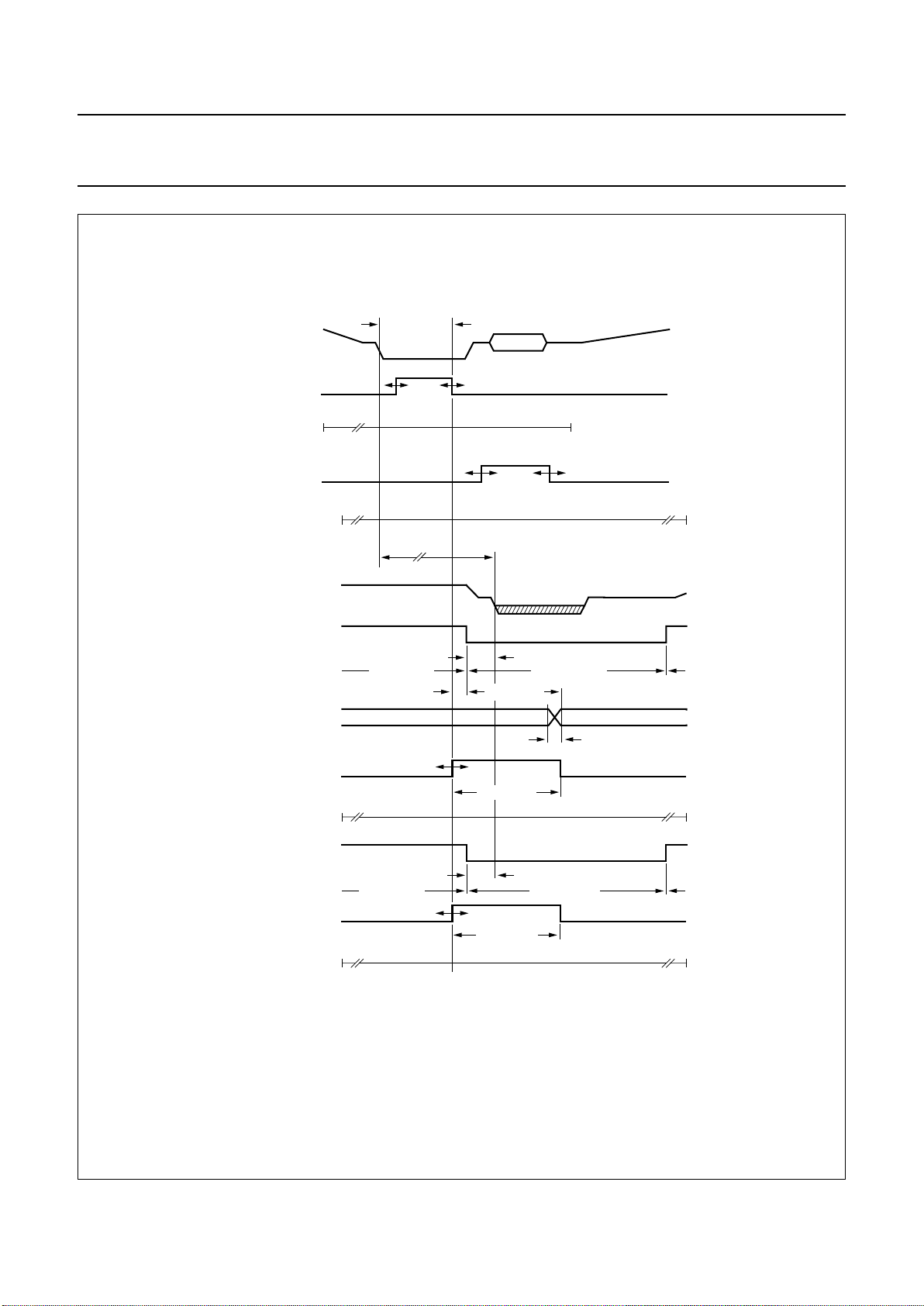
Fig.11 Horizontal timing.
(1) See Table 1.
HRMV = 1 and HRFS = 0.
handbook, full pagewidth
0
+117
−118
+97
−97
MGC830
CVBS
HSY
HCL
62 × 2/LLC
30 × 2/LLC
Y output
HREF (50 Hz)
18 × 2/LLC
768 × 2/LLC
176 × 2/LLC
18 × 2/LLC
140 × 2/LLC
640 × 2/LLC
64 × 2/LLC
burst
PLIN (50 Hz)
processing delay CVBS−>YUV
0
+191
−64
0
4/LLC
HREF (60 Hz)
HS (60 Hz)
HS (50 Hz)
programming range
(step size: 8/LLC)
+127
−128
HCL
programming range
(step size: 2/LLC)
HSY
programming range
(step size: 2/LLC)
HS (60 Hz)
programming range
(step size: 8/LLC)
HS (50 Hz)
94 × 2/LLC
64 × 2/LLC
(1)

1995 Oct 18 23
Philips Semiconductors Product specification
One Chip Front-end 1 (OCF1) SAA7110; SAA7110A
Fig.12 HREF timing.
handbook, full pagewidth
01234
U0 V0 U1 V1 U2
END OF ACTIVE LINE
START OF ACTIVE LINE
767766765764763
U766 V766V764U764V762
639638637636635
U638 V638
MGC831
V636U636V634
ONE BUS CYCLE
LL27
CREF
HREF
Yn
Yn
(50 Hz)
UVn
Yn
(60 Hz)
UVn
UVn
HREF
INTERNAL
BUS CLOCK
 Loading...