

Philips SAA7102E, SAA7102H, SAA7103E, SAA7103H Datasheet

INTEGRATED CIRCUITS
DATA SH EET
SAA7102; SAA7103
Digital video encoder
Product specification
File under Integrated Circuits, IC22
2001 Sep 25

Philips Semiconductors Product specification
Digital video encoder SAA7102; SAA7103
CONTENTS
1 FEATURES
2 GENERAL DESCRIPTION
3 ORDERING INFORMATION
4 QUICK REFERENCE DATA
5 BLOCK DIAGRAM
6 PINNING
7 FUNCTIONAL DESCRIPTION
7.1 Reset conditions
7.2 Input formatter
7.3 RGB LUT
7.4 Cursor insertion
7.5 RGB Y-CB-CR matrix
7.6 Horizontal scaler
7.7 Vertical scaler and anti-flicker filter
7.8 FIFO
7.9 Border generator
7.10 Oscillator and Discrete Time Oscillator (DTO)
7.11 Low-pass Clock Generation Circuit (CGC)
7.12 Encoder
7.13 RGB processor
7.14 Triple DAC
7.15 Timing generator
7.16 I2C-bus interface
7.17 Programming the SAA7102; SAA7103
7.18 Input levels and formats
7.19 Bit allocation map
7.20 I2C-bus format
7.21 Slave receiver
7.22 Slave transmitter
8 BOUNDARY SCAN TEST
8.1 Initialization of boundary scan circuit
8.2 Device identification codes
9 LIMITING VALUES
10 THERMAL CHARACTERISTICS
11 CHARACTERISTICS
11.1 Teletext timing
12 APPLICATION INFORMATION
12.1 Analog output voltages
12.2 Suggestions for a board layout
13 PACKAGE OUTLINES
14 SOLDERING
14.1 Introduction to soldering surface mount
packages
14.2 Reflow soldering
14.3 Wave soldering
14.4 Manual soldering
14.5 Suitability of surface mount IC packages for
wave and reflow soldering methods
15 DATA SHEET STATUS
16 DEFINITIONS
17 DISCLAIMERS
18 PURCHASE OF PHILIPS I2C COMPONENTS
2001 Sep 25 2

Philips Semiconductors Product specification
Digital video encoder SAA7102; SAA7103
1 FEATURES
• Digital PAL/NTSC encoder with integrated high quality
scaler and anti-flicker filter for TV output from a PC
• 27 MHz crystal-stable subcarrier generation
• Maximum graphics pixelclock 45 MHz at double edged
clocking, synthesized on-chip or from external source
• Up to 800 × 600 graphics data at 60 Hz or 50 Hz with
programmable underscan range
• Three Digital-to-Analog Converters (DACs) at 27 MHz
sample rate for CVBS (BLUE, CB), VBS (GREEN,
CVBS) and C (RED, CR) (signals in parenthesis are
optional); all at 10-bit resolution
• Non-interlaced CB-Y-CR or RGB input at maximum
4:4:4 sampling
• Downscaling from 1 : 1 to 1 : 2 and up to 20% upscaling
• Optional interlaced CB-Y-CRinput Digital Versatile Disk
(DVD)
• Optional non-interlaced RGB output to drive second
VGA monitor (bypass mode, maximum 45 MHz)
• 3 × 256 bytes RGB Look-Up Table (LUT)
• Support for hardware cursor
• Programmable border colour of underscan area
• On-chip 27 MHz crystal oscillator (3rd-harmonic or
fundamental 27 MHz crystal)
• Fast I2C-bus control port (400 kHz)
• Encoder can be master or slave
• Programmable horizontal and vertical input
synchronization phase
• Programmable horizontal sync output phase
• Internal Colour Bar Generator (CBG)
• Optional support of various Vertical Blanking Interval
(VBI) data insertion
• Macrovision Pay-per-View copy protection system
rev. 7.01and rev. 6.1 as option; this appliestoSAA7102
only. The device is protected by USA patent numbers
4631603, 4577216 and 4819098 and other intellectual
property rights. Use of the Macrovision anti-copy
process in the device is licensed for non-commercial
home use only. Reverse engineering or disassembly is
prohibited. Please contact your nearest Philips
Semiconductors sales office for more information.
• Power-save modes
• Joint Test Action Group (JTAG) boundary scan test
• Monolithic CMOS 3.3 V device, 5 V tolerant I/Os
• QFP44 and BGA156 packages
• Same footprint as SAA7108E; SAA7109E.
2 GENERAL DESCRIPTION
The SAA7102; SAA7103 is used to encode PC graphics
data at maximum 800 × 600 resolution to PAL (50 Hz) or
NTSC (60 Hz) video signals. A programmable scaler and
interlacer ensures properly sized and flicker-free TV
display as CVBS or S-video output.
Alternatively, the three Digital-to-Analog Converters
(DACs) can output RGB signals together with a TTL
composite sync to feed SCART connectors.
When the scaler/interlacer is bypassed, a second VGA
monitor can be connected to the RGB outputs and
separate H and V-syncs as well, thereby serving as an
auxiliary monitor at maximum 800 × 600 resolution/60 Hz
(PIXCLK < 45 MHz).
The device includes a sync/clock generator and on-chip
DACs.
2001 Sep 25 3

Philips Semiconductors Product specification
Digital video encoder SAA7102; SAA7103
3 ORDERING INFORMATION
TYPE NUMBER
PACKAGE
NAME DESCRIPTION VERSION
SAA7102E BGA156 plastic ball grid array package; 156 balls; body
SAA7103E
15 × 15 × 1.15 mm
SAA7102H QFP44 plastic quad flat package; 44 leads (lead length 1.3 mm);
SAA7103H
body 10 × 10 × 1.75 mm
SOT472-1
SOT307-2
4 QUICK REFERENCE DATA
SYMBOL PARAMETER MIN. TYP. MAX. UNIT
V
V
I
DDA
I
DDD
V
V
DDA
DDD
i
o(p-p)
analog supply voltage 3.15 3.3 3.45 V
digital supply voltage 3.0 3.3 3.6 V
analog supply current 1 110 140 mA
digital supply current 1 70 90 mA
input signal voltage levels TTL compatible
analog CVBS output signal voltage for a 100/100
− 1.23 − V
colour bar at 75/2 Ω load (peak-to-peak value)
R
L
ILE
DLE
T
amb
lf(DAC)
lf(DAC)
load resistance − 37.5 −Ω
low frequency integral linearity error of DACs −−±3 LSB
low frequency differential linearity error of DACs −−±1 LSB
ambient temperature 0 − 70 °C
2001 Sep 25 4

This text is here in white to force landscape pages to be rotated correctly when browsing through the pdf in the Acrobat reader.This text is here in
_white to force landscape pages to be rotated correctly when browsing through the pdf in the Acrobat reader.This text is here inThis text is here in
white to force landscape pages to be rotated correctly when browsing through the pdf in the Acrobat reader. white to force landscape pages to be ...
2001 Sep 25 5
5 BLOCK DIAGRAM
Philips Semiconductors Product specification
Digital video encoder SAA7102; SAA7103
PD11 to
PD0
PIXCLKI
PIXCLKO
4 to 1,
44 to 41,
16 to 19
15
20
V
DDD1
10
INPUT
FORMATTER
DECIMATOR
4 : 4 : 4 to 4 : 2 : 2
(OR BYPASS)
BORDER
GENERATOR
CGC
LOW-PASS
V
SSD1
9
TTX_SRES
V
DDD2
V
40
RGB LUT
(OR BYPASS)
HORIZONTAL
SCALER
VIDEO
ENCODER
OSCILLATOR/
XTALI
27 MHz
SSD2
DTO
V
DDA1
V
SSA1
29
INSERTION
VERTICAL
SCALER AND
ANTI-FLICKER
SAA7102H
SAA7103H
GENERATOR
13343523
VSVGC
FSVGC
DUMP
33
CURSOR
FILTER
TIMING
14 21
CBO
RSET
32
31
HSVGC
TTXRQ_XCLKO2
TRST
TDI
38
TCLK
8
37
RGB TO Y-CB-C
MATRIX
(OR BYPASS)
FIFO
TRIPLE
DAC
I2C-BUS
CONTROL
11 522 24
12
SDA
SCL
TDO
7
R
RESET
TMS
6
30
BLUE_CB_CVBS
28
GREEN_VBS_CVBS
27
RED_CR_C
26
HSM_CSYNC
25
VSM
MHB963
V
DDA2
39
36
XTAL
handbook, full pagewidth
Fig.1 Block diagram.

Philips Semiconductors Product specification
Digital video encoder SAA7102; SAA7103
6 PINNING
SYMBOL
PIN
BGA156 QFP44
PIN
TYPE
(1)
DESCRIPTION
PD8 B2 1 I see Tables 25 to 29 for pin assignment
PD9 B1 2 I see Tables 25 to 29 for pin assignment
PD10 C2 3 I see Tables 25 to 29 for pin assignment
PD11 C1 4 I see Tables 25 to 29 for pin assignment
RESET D2 5 I reset input; active LOW
TMS D3 6 I test mode select input for Boundary Scan Test (BST); note 2
TDO D1 7 O test data output for BST; note 2
TCLK E1 8 I test clock input for BST; note 2
V
SSD1
V
DDD1
SCL E2 11 I I
SDA G2 12 I/O I
E4 9 S digital ground 1 (peripheral cells)
F4 10 S digital supply voltage 1 (3.3 V, peripheral cells)
2
C-bus serial clock input
2
C-bus serial data input/output
FSVGC G1 13 I/O frame synchronization output to Video Graphics Controller
(VGC) (optional input)
VSVGC F1 14 I/O vertical synchronization output to VGC (optional input)
PIXCLKI F2 15 I pixel clock input (looped through)
PD3 F3 16 I MSB − 4 with C
-Y-CR 4 : 2 : 2; see Tables 25 to 29 for pin
B
assignment
PD2 H1 17 I MSB − 5 with C
-Y-CR 4 : 2 : 2; see Tables 25 to 29 for
B
pin assignment
PD1 H2 18 I MSB − 6 with C
-Y-CR 4 : 2 : 2; see Tables 25 to 29 for
B
pin assignment
PD0 H3 19 I MSB − 7 with C
-Y-CR 4 : 2 : 2; see Tables 25 to 29 for
B
pin assignment
PIXCLKO G4 20 O pixel clock output to VGC
CBO G3 21 O composite blanking output to VGC; active LOW
HSVGC E3 22 I/O horizontal synchronization output to VGC (optional input)
TTX_SRES C3 23 I teletext input or sync reset input
TTXRQ_XCLKO2 C4 24 O teletext request output or 13.5 MHz clock output of the crystal
oscillator
VSM D7 25 O vertical synchronization output to monitor (non-interlaced
auxiliary RGB)
HSM_CSYNC D8 26 O horizontal synchronization output to monitor (non-interlaced
auxiliary RGB) or composite sync for RGB-SCART
RED_CR_C C8 27 O analog output of RED or C
or C signal
R
GREEN_VBS_CVBS C7 28 O analog output of GREEN or VBS or CVBS signal
V
DDA1
A10,B9,
29 S analog supply voltage 1 (3.3 V for DACs)
C9, D9
BLUE_CB_CVBS C6 30 O analog output of BLUE or C
or CVBS signal
B
2001 Sep 25 6

Philips Semiconductors Product specification
Digital video encoder SAA7102; SAA7103
SYMBOL
PIN
BGA156 QFP44
PIN
TYPE
(1)
DESCRIPTION
RSET A9 31 O DAC reference pin; connected via 1 kΩ resistor to analog ground
(do not use capacitor in parallel with 1 kΩ resistor)
DUMP A7, B7 32 O DAC reference pin; connected via 12 Ω resistor to analog
ground
V
SSA1
A8, B8 33 S analog ground 1
XTALO A6 34 O crystal oscillator output
XTALI A5 35 I crystal oscillator input
V
DDA2
B6, D6 36 S analog supply voltage 2 (3.3 V for DACs and oscillator)
TRST A4 37 I test reset input for BST; active LOW; notes 3 and 4
TDI B5 38 I test data input for BST; note 2
V
SSD2
V
DDD2
PD4 A3 41 I MSB − 3 with C
C5, D5 39 S digital ground 2
D4 40 S digital supply voltage 2 (3.3 V, core)
-Y-CR 4 : 2 : 2; see Tables 25 to 29 for pin
B
assignment
PD5 B3 42 I MSB − 2 with C
-Y-CR 4 : 2 : 2; see Tables 25 to 29 for pin
B
assignment
PD6 B4 43 I MSB − 1 with C
-Y-CR 4 : 2 : 2; see Tables 25 to 29 for pin
B
assignment
PD7 A2 44 I MSB with C
-Y-CR 4 : 2 : 2; see Tables 25 to 29 for pin
B
assignment
Notes
1. Pin type: I = input, O = output, S = supply.
2. In accordance with the
“IEEE1149.1”
standard the pins TDI, TMS, TCLK and TRST are input pins with an internal
pull-up resistor and TDO is a 3-state output pin.
3. For board design without boundary scan implementation connect TRST to ground.
4. This pin provides easy initialization of the Boundary Scan Test (BST) circuit. TRST can be used to force the Test
Access Port (TAP) controller to the TEST_LOGIC_RESET state (normal operation) at once.
2001 Sep 25 7

Philips Semiconductors Product specification
Digital video encoder SAA7102; SAA7103
Table 1 Pin assignment SAA7102E; SAA7103E (top view)
1 2 3 4 5 6 7 8 9 1011121314
A PD7 PD4 TRST XTALI XTALO DUMP V
B PD9 PD8 PD5 PD6 TDI V
C PD11 PD10 TTX_
SRES
D TDO RESET TMS V
TTXRQ_
V
SSD2
XCLKO2
DDD2VSSD2VDDA2
BLUE_
CB_
CVBS
DDA2
DUMP V
GREEN_
VBS_
CVBS
VSM HSM_
CSYNC
E TCLK SCL HSVGC V
F VSVGCPIXCLKI PD3 V
SSD1
DDD1
G FSVGC SDA CBO PIXCLKO
H PD2 PD1 PD0
J
RSET V
SSA1
SSA1VDDA1
RED_
V
CR_
C
V
DDA1
DDA1
DDA1
K
L
M
N
P
2001 Sep 25 8

Philips Semiconductors Product specification
Digital video encoder SAA7102; SAA7103
MHB907
handbook, halfpage
P
N
M
L
K
J
H
G
F
E
D
C
B
A
234567891011121314
1
SAA7102E
SAA7103E
handbook, full pagewidth
PD8
PD9
PD10
PD11
RESET
TMS
TDO
TCLK
V
SSD1
V
DDD1
SCL
Fig.2 Pin configuration (SAA7102E; SAA7103E).
PD7
PD6
PD5
44
43
42
1
2
3
4
5
6
7
8
9
10
11
DDD2VSSD2
PD4
V
41
40
SAA7102H
SAA7103H
TDI
39
38
TRST
37
DDA2
V
36
XTALI
35
XTALO
34
33
V
SSA1
32
DUMP
31
RSET
30
BLUE_CB_CVBS
V
29
DDA1
28
GREEN_VBS_CVBS
27
RED_CR_C
26
HSM_CSYNC
25
VSM
24
TTXRQ_XCLKO2
23
TTX_SRES
12
13
14
15
16
SDA
FSVGC
VSVGC
PD3
PIXCLKI
Fig.3 Pin configuration (SAA7102H; SAA7103H).
2001 Sep 25 9
17
PD2
18
PD1
19
PD0
20
21
CBO
PIXCLKO
22
MHB908
HSVGC

Philips Semiconductors Product specification
Digital video encoder SAA7102; SAA7103
7 FUNCTIONAL DESCRIPTION
The digital video encoder encodes digital luminance and
colour difference signals (CB-Y-CR) or digital RGB signals
into analog CVBS, S-video and, optionally, RGB or
CR-Y-CB signals. NTSC M, PAL B/G and sub-standards
are supported.
The SAA7102; SAA7103 can be directly connected to a
PC video graphics controller with a maximum resolution of
800 × 600 at a 50 or 60 Hz frame rate. A programmable
scalerscales the computer graphics picture sothatit will fit
into a standard TV screen with an adjustable underscan
area.Non-interlaced-to-interlaced conversion is optimized
with an adjustable anti-flicker filter for a flicker-free display
at a very high sharpness.
Besides the most common 16-bit 4 :2:2 CB-Y-CR input
format (using 8 pins with double edge clocking), other
CB-Y-CR and RGB formats are also supported; see
Tables 25 to 29.
Acomplete3 × 256bytesLook-Up Table (LUT), which can
be used, for example, as a separate gamma corrector, is
locatedin the RGB domain; it canbeloaded either through
the video input port PD (Pixel Data) or via the I2C-bus.
The SAA7102; SAA7103 supports a 32 × 32 × 2-bit
hardware cursor, the pattern of which can also be loaded
through the video input port or via the I2C-bus.
For ease of analog post filtering the signals are twice
oversampled to 27 MHz before digital-to-analog
conversion.
The total filter transfer characteristics (scaler and
anti-flicker filter are not taken into account) are illustrated
in Figs 4 to 8. All three DACs are realized with full 10-bit
resolution. The CR-Y-CB to RGB dematrix can be
bypassed (optionally) in order to provide the upsampled
CR-Y-CB input signals.
The8-bitmultiplexedCB-Y-CRformatsare
(D1 format) compatible, but the SAV and EAV codes can
be decoded optionally, when the device is operated in
slave mode. For assignment of the input data to the rising
or falling clock edge see Tables 25 to 29.
In order to display interlaced RGB signals through a
euro-connector TV set, a separate digital composite sync
signal (pin 26) can be generated; it can be advanced up to
31 periods of the 27 MHz crystal clock in order to be
adapted to the RGB processing of a TV set.
The SAA7102; SAA7103 synthesizes all necessary
internal signals, colour subcarrier frequency and
synchronization signals from that clock.
Wide screen signalling data can be loaded via the I2C-bus
and is inserted into line 23 for standards using a 50 Hz
field rate.
“ITU-R BT.656”
It is also possible to encode interlaced 4 :2:2 video
signals such as PC-DVD; for that the anti-flicker filter, and
in most cases the scaler, will simply be bypassed.
Besides the applications for video output, the SAA7102;
SAA7103 can also be used for generating a kind of
auxiliary VGA output, when the RGB non-interlaced input
signal is fed to the DACs. This may be of interest for
example, when the graphics controller provides a second
graphics window at its video output port.
The basic encoder function consists of subcarrier
generation, colour modulation and insertion of
synchronization signals at a crystal-stable clock rate of
13.5 MHz (independent of the actual pixel clock used at
the input side), corresponding to an internal 4 :2:2
bandwidth in the luminance/colour difference domain.
Luminance and chrominance signals are filtered in
accordance with the standard requirements of
and
“ITU-R BT.470-3”
.
“RS-170-A”
VPS data for program dependent automatic start and stop
of such featured VCRs is loadable via the I2C-bus.
The IC also contains Closed Caption and extended data
servicesencoding(line 21),andsupportsteletext insertion
fortheappropriatebitstreamformatata27 MHz clock rate
(see Fig.14). It is also possible to load data for the copy
generation management system into line 20 of every field
(525/60 line counting).
A number of possibilities are provided for setting different
video parameters such as:
• Black and blanking level control
• Colour subcarrier frequency
• Variable burst amplitude etc.
2001 Sep 25 10

Philips Semiconductors Product specification
Digital video encoder SAA7102; SAA7103
7.1 Reset conditions
To activate the reset a pulse at least of 2 crystal clocks
duration is required.
During reset (RESET = LOW) plus an extra 32 crystal
clock periods, FSVGC, VSVGC, CBO, HSVGC and
TTX_SRES are set to input mode and HSM_CSYNC and
VSM are set to 3-state. A reset also forces the I2C-bus
interface to abort any running bus transfer and sets it into
receive condition.
After reset, the state of the I/Os and other functions is
defined by the strapping pins until an I2C-bus access
redefines the corresponding registers; see Table 2.
Table 2 Strapping pins
PIN TIED PRESET
FSVGC (pin 13) LOW NTSC M encoding, PIXCLK
fits to 640 × 480 graphics
input
HIGH PAL B/G encoding, PIXCLK
fits to 640 × 480 graphics
input
VSVGC (pin 14) LOW 4:2:2 Y-C
input (format 0)
HIGH 4:4:4 RGB graphics input
(format 3)
CBO (pin 21) LOW input demultiplex phase:
LSB=LOW
HIGH input demultiplex phase:
LSB = HIGH
HSVGC (pin 22) LOW input demultiplex phase:
MSB = LOW
HIGH input demultiplex phase:
MSB = HIGH
TTXRQ_XCLKO2
(pin 24)
LOW slave (FSVGC, VSVGC and
HSVGC are inputs, internal
colour bar is active)
HIGH master (FSVGC, VSVGC
and HSVGC are outputs)
B-CR
graphics
If Y-CB-CR is being applied as a 27 Mbyte/s data stream,
the output of the input formatter can be used directly to
feed the video encoder block.
7.3 RGB LUT
The three 256 byte RAMs of this block can be addressed
by three 8-bit wide signals, thus it can be used to build any
transformation, e.g. a gamma correction for RGB signals.
In the event that the indexed colour data is applied, the
RAMs are addressed in parallel.
The LUTs can eitherbe loaded by an I2C-bus write access
or can be part of the pixel data input through the PD port.
Inthe latter case, 256 × 3 bytesfor the R, G andB LUT are
expected at the beginning of the input video line, two lines
before the line that has been defined as first active line,
until the middle of the line immediately preceding the first
active line. The first 3 bytes represent the first RGB LUT
data, and so on.
7.4 Cursor insertion
The cursor bit map is set up as follows: each pixel
occupies 2 bits. The meaning of these bits depends on the
CMODE I2C-bus register as described in Table 5.
Transparent means that the input pixels are passed
through, the ‘cursor colours’ can be programmed in
separate registers.
The bit map is stored with 4 pixels per byte, aligned to the
least significant bit. So the first pixel is in bits 0 and 1, the
next pixel in bits 3 and 4 and so on. The first index is the
column, followed by the row; index 0,0 is the upper left
corner.
Table 3 Layout of a byte in the cursor bit map
D7 D6 D5 D4 D3 D2 D1 D0
pixel n + 3 pixel n + 2 pixel n + 1 pixel n
D1 D0 D1 D0 D1 D0 D1 D0
7.2 Input formatter
The input formatter converts all accepted PD input data
formats, either RGB or Y-CB-CR, to a common internal
RGB or Y-CB-CR data stream.
When double-edge clocking is used, the data is internally
split into portions PPD1 and PPD2. The clock edge
assignment must be set according to the I2C-bus control
bits EDGE1 and EDGE2 for correct operation.
2001 Sep 25 11

Philips Semiconductors Product specification
Digital video encoder SAA7102; SAA7103
Table 4 Cursor bit map
BYTE D7 D6 D5 D4 D3 D2 D1 D0
0row0
column 3
1row0
column 7
2row0
column
11
... ... ... ... ...
6row0
column
27
7row0
column
31
... ... ... ... ...
254 row 31
column
27
255 row 31
column
31
Table 5 Cursor modes
CURSOR
PATTERN
00 second cursor colour second cursor colour
01 first cursor colour first cursor colour
10 transparent transparent
11 inverted input auxiliary cursor
7.5 RGB Y-C
RGB input signals to be encoded to PAL or NTSC are
converted to the Y-C
colour difference signals are fed through low-pass filters
and formatted to a ITU-R BT.601 like 4 : 2 : 2 data stream
for further processing.
row 0
column 2
row 0
column 6
row 0
column
10
row 0
column
26
row 0
column
30
row 31
column
26
row 31
column
30
CURSOR MODE
CMODE = 0 CMODE = 1
matrix
B-CR
colour space in this block. The
B-CR
row 0
column 1
row 0
column 5
row 0
column 9
row 0
column
25
row 0
column
29
row 31
column
25
row 31
column
29
colour
row 0
column 0
row 0
column 4
row 0
column 8
row 0
column
24
row 0
column
28
row 31
column
24
row 31
column
28
7.6 Horizontal scaler
The high quality horizontal scaler operates on the 4 : 2 : 2
data stream. Its control engines compensate the colour
phase offset automatically.
The scaler starts processing after a programmable
horizontal offset and continues with a number of input
pixels. Each input pixel is a programmable fraction of the
current output pixel (XINC/4096). A special case is
XINC = 0, this sets the scaling factor to 1.
If the SAA7102; SAA7103 input data is in accordance with
“ITU-R BT.656”
event, XINC needs to be set to 2048 for a scaling factor
of 1. With higher values, upscaling will occur.
The phase resolution of the circuit is 12 bits, giving a
maximum offset of 0.2 after 800 input pixels. Small FIFOs
rearrange a 4 : 2 : 2 data stream at the scaler output.
7.7 Vertical scaler and anti-flicker filter
The functions scaling, Anti-Flicker Filter (AFF) and
re-interlacing are implemented in the vertical scaler.
Besides the entire input frame, it receives the first and last
lines of the border to allow anti-flicker filtering.
Thecircuitgeneratestheinterlacedoutputfieldsbyscaling
down the input frames with different offsets for odd and
even fields. Increasing the YSKIP setting reduces the
anti-flicker function. A YSKIP value of 4095 switches it off;
see Table 94.
Theprogrammingissimilartothehorizontalscaler. For the
re-interlacing,the resolutions of the offsetregisters are not
sufficient, so the weighting factors for the first lines can
also be adjusted. YINC = 0 sets the scaling factor to 1;
YIWGTO and YIWGTE must not be 0.
Dueto the re-interlacing, the circuit can perform upscaling.
The maximum factor depends on the setting of the
anti-flicker function and can be derived from the formulae
given in Section 7.17.
, the scaler enters another mode. In this
The matrix and formatting blocks can be bypassed for
Y-CB-CR graphics input.
WhentheauxiliaryVGAmodeisselected,theoutputofthe
cursor insertion block is immediately directed to the triple
DAC.
2001 Sep 25 12

Philips Semiconductors Product specification
Digital video encoder SAA7102; SAA7103
7.8 FIFO
The FIFO acts as a buffer to translate from the PIXCLK
clock domain to the XTAL clock domain. The write clock is
PIXCLK and the read clock is XTAL. An underflow or
overflow condition can be detected via the I2C-bus read
access.
In order to avoid underflows and overflows, it is essential
that the frequency of the synthesized PIXCLK matches to
the input graphics resolution and the desired scaling
factor. It is suggested to refer to Tables 6 to 23 for some
representative combinations.
7.9 Border generator
When the graphics picture is to be displayed as interlaced
PAL, NTSC, S-video or RGB on a TV screen, it is desired
in many cases not to lose picture information due to the
inherent overscanning of a TV set. The desired amount of
underscan area, which is achieved through appropriate
scaling in the vertical and horizontal direction, can be filled
in the border generator with an arbitrary true colour tint.
7.10 Oscillator and Discrete Time Oscillator (DTO)
The master clock generation is realized as a 27 MHz
crystal oscillator, which can operate with either a
fundamental wave crystal or a 3rd-harmonic crystal.
The crystal clock supplies the DTO of the pixel clock
synthesizer, the video encoder and the I2C-bus control
block. It also usually supplies the triple DAC, with the
exceptionof the auxiliary VGA mode, where thetripleDAC
is clocked by the pixel clock (PIXCLK).
The DTO can be programmed to synthesize all relevant
pixel clock frequencies between circa 18 and 44 MHz.
7.11 Low-pass Clock Generation Circuit (CGC)
This block reduces the phase jitter of the synthesized pixel
clock. It works as a tracking filter for all relevant
synthesized pixel clock frequencies.
7.12 Encoder
7.12.1 VIDEO PATH
The encoder generates luminance and colour subcarrier
output signals from the Y, CBand CR baseband signals,
which are suitable for use as CVBS or separate Y and C
signals.
Input to the encoder, at 27 MHz clock (e.g. DVD), is either
originated from computer graphics at pixel clock, fed
throughtheFIFOandbordergenerator,oraITU-R BT.656
style signal.
Luminance is modified in gain and in offset (the offset is
programmable in a certain range to enable different black
level set-ups). A blanking level can be set after insertion of
a fixed synchronization pulse tip level, in accordance with
standard composite synchronization schemes. Other
manipulations used for the Macrovision anti-taping
process, such as additional insertion of AGC super-white
pulses (programmable in height), are supported by the
SAA7102 only.
To enable easy analog post filtering, luminance is
interpolated from a 13.5 MHz data rate to a 27 MHz data
rate, thereby providing luminance in a 10-bit resolution.
The transfer characteristics of the luminance interpolation
filter are illustrated in Figs 7 and 8. Appropriate transients
at start/end of active video and for synchronization pulses
are ensured.
Chrominance is modified in gain (programmable
separately for CBand CR), and a standard dependent
burst is inserted, before baseband colour signals are
interpolated from a 6.75 MHz data rate to a 27 MHz data
rate. One of the interpolation stages can be bypassed,
thus providing a higher colour bandwidth, which can be
usedfortheY and Coutput.Thetransfer characteristics of
the chrominance interpolation filter are illustrated in
Figs 4 and 5.
The amplitude (beginning and ending) of the inserted
burst, is programmable in a certain range that is suitable
for standard signals and for special effects. After the
succeeding quadrature modulator, colour is provided on
the subcarrier in 10-bit resolution.
The numeric ratio between the Y and C outputs is in
accordance with the standards.
7.12.2 TELETEXT INSERTION AND ENCODING (NOT
SIMULTANEOUSLY WITH REAL
Pin TTX_SRES receives a WST or NABTS teletext
bitstream sampled at the crystal clock. At each rising edge
of the output signal (TTXRQ) a single teletext bit has to be
provided after a programmable delay at input pin
TTX_SRES.
-TIME CONTROL)
2001 Sep 25 13

Philips Semiconductors Product specification
Digital video encoder SAA7102; SAA7103
Phase variant interpolation is achieved on this bitstream in
the internal teletext encoder, providing sufficient small
phase jitter on the output text lines.
TTXRQ_XCLKO2 provides a fully programmable request
signal to the teletext source, indicating the insertion period
of bitstream at lines which can be selected independently
for both fields. The internal insertion window for text is set
to 360 (PAL WST), 296 (NTSC WST) or 288 (NABTS)
teletext bits including clock run-in bits. The protocol and
timing are illustrated in Fig.14.
Alternatively, this pin can be provided with a buffered
crystal clock (XCLK) of 13.5 MHz.
7.12.3 VIDEO PROGRAMMING SYSTEM (VPS) ENCODING
Five bytes of VPS information can be loaded via the
I2C-bus and will be encoded in the appropriate format into
line 16.
7.12.4 CLOSED CAPTION ENCODER
Using this circuit, data in accordance with the specification
of Closed Caption or extended data service, delivered by
the control interface, can be encoded (line 21). Two
dedicated pairs of bytes (two bytes per field), each pair
preceded by run-in clocks and framing code, are possible.
Theactual line number in which datais to be encoded, can
be modified in a certain range.
The data clock frequency is in accordance with the
definition for NTSC M standard 32 times horizontal line
frequency.
DataLOWattheoutputoftheDACscorresponds to 0 IRE,
data HIGH at the output of the DACs corresponds to
approximately 50 IRE.
Itis also possible to encode Closed Caption data for50 Hz
field frequencies at 32 times the horizontal line frequency.
7.12.5 ANTI-TAPING (SAA7102 ONLY)
For more information contact your nearest Philips
Semiconductors sales office.
7.13 RGB processor
This block contains a dematrix in order to produce RED,
GREEN and BLUE signals to be fed to a SCART plug.
Before Y, CBand CR signals are de-matrixed, individual
gain adjustment for Y and colour difference signals and
2 times oversampling for luminance and 4 times
oversampling for colour difference signals is performed.
The transfer curves of luminance and colour difference
components of RGB are illustrated in Figs 8 and 9.
7.14 Triple DAC
Both Y and C signals are converted from digital-to-analog
in a 10-bit resolution at the output of the video encoder.
Y and C signals are also combined into a 10-bit CVBS
signal.
The CVBS output signal occurs with the same processing
delay as the Y, C and optional RGB or CR-Y-CB outputs.
Absolute amplitude at the input of the DAC for CVBS is
reduced by15⁄16with respect to Y and C DACs to make
maximum use of the conversion ranges.
RED, GREEN and BLUE signals are also converted from
digital-to-analog, each providing a 10-bit resolution.
The reference currents of all three DACs can be adjusted
individually in order to adapt for different output signals.
In addition, all reference currents can be adjusted
commonly to compensate for small tolerances of the
on-chip band gap reference voltage.
Alternatively, all currents can be switched off to reduce
power dissipation.
All three outputs can be used to sense for an external load
(usually 75 Ω) during a pre-defined output. A flag in the
I2C-bus status byte reflects whether a load is applied or
not.
If the SAA7102; SAA7103 is required to drive a second
(auxiliary) VGA monitor, the DACs receive the signal
directly from the cursor insertion block. In this event, the
DACs are clocked at the incoming PIXCLKI instead of the
27 MHz crystal clock used in the video encoder.
7.15 Timing generator
The synchronization of the SAA7102; SAA7103 is able to
operate in two modes; slave mode and master mode.
In slave mode, the circuit accepts sync pulses on the
bidirectional FSVGC (frame sync), VSVGC (vertical sync)
and HSVGC (horizontal sync) pins: the polarities of the
signals can be programmed. The frame sync signal is only
necessary when the input signal is interlaced, in other
casesitmaybeomitted.Iftheframesyncsignalispresent,
it is possible to derive the vertical andthe horizontal phase
from it by setting the HFS and VFS bits. HSVGC and
VSVGC are not necessary in this case, so it is possible to
switch the pins to output mode.
Alternatively, the device can be triggered by auxiliary
codes in a ITU-R BT.656 data stream via PD7 to PD0.
2001 Sep 25 14

Philips Semiconductors Product specification
Digital video encoder SAA7102; SAA7103
Only vertical frequencies of 50 and 60 Hz are allowed with
the SAA7102; SAA7103. In slave mode, it is not possible
to lock the encoders colour carrier to the line frequency
with the PHRES bits.
In the (more common) master mode, the time base of the
circuit is continuously free-running. The IC can output a
frame sync at pin FSVGC, a vertical sync at pin VSVGC, a
horizontal sync at pin HSVGC and a composite blanking
signal at pin CBO. All of these signals are defined in the
PIXCLK domain. The duration of HSVGC and VSVGC are
fixed,theyare64 clocks for HSVGC and 1 line for VSVGC.
The leading slopes are in phase and the polarities can be
programmed.
The input line length can be programmed. The field length
is always derived from the field length of the encoder and
the pixel clock frequency that is being used.
CBO acts as a data request signal. The circuit accepts
input data at a programmable number of clocks after CBO
goes active. This signal is programmable and it is possible
to adjust the following (see Figs 12 and 13):
• The horizontal offset
• The length of the active part of the line
• The distance from active start to first expected data
• The vertical offset separately for odd and even fields
• The number of lines per input field.
In most cases, the vertical offsets for odd and even fields
are equal. If they are not, then the even field will start later.
The SAA7102; SAA7103 will also request the first input
lines in the even field, the total number of requested lines
will increase by the difference of the offsets.
As stated above, the circuit can be programmed to accept
the look-up and cursor data in the first 2 lines of each field.
The timing generator provides normal data request pulses
fortheselines;thedurationisthesameasforregularlines.
The additional request pulses will be suppressed with
LUTL set to logic 0; see Table 104. The other vertical
timings do not change in this case, so the first active line
can be number 2, counted from 0.
2
7.16 I
C-bus interface
The register bit map consists of an RGB Look-Up Table
(LUT), a cursor bit map and control registers. The LUT
containsthree banks of 256 bytes, whereeach RGB triplet
isassigned to one address. Thus a write access needsthe
LUT address and three data bytes following subaddress
FFH. For further write access auto-incrementing of the
LUT address is performed. The cursor bit map access is
similar to the LUT access but contains only a single byte
per address.
2
The I
C-bus slave address is defined as 88H.
7.17 Programming the SAA7102; SAA7103
In order to program the SAA7102; SAA7103 it is first
necessary to determine the input and output field timings.
The timings are controlled by decoding binary counters
that index the position in the current line and field
respectively. In both cases, 0 means the start of the sync
pulse.
At 60 Hz, the first visible pixel has the index 256,
710 pixels can be encoded; at 50 Hz, the index is 284,
702 pixels can be visible. Some variables are defined
below:
• InPix: the number of active pixels per input line
• InPpl: the length of the entire input line in pixel clocks
• InLin: the number of active lines per input field/frame
• TPclk: the pixel clock period
• OutPix: the number of active pixels per output line
• OutLin: the number of active lines per output field
• TXclk: the encoder clock period (37.037 ns).
Theoutput lines should be centred onthescreen. It should
be noted that the encoder has 2 clocks per pixel;
see Table 71.
ADWHS = 256 + 710 − OutPix (60 Hz);
ADWHS = 284 + 702 − OutPix (50 Hz);
ADWHE = ADWHS + OutPix × 2 (all frequencies)
For vertical, the procedure is the same. At 60 Hz, the first
line with video information is number 19, 240 lines can be
active. For 50 Hz, the numbers are 23 and 287;
see Table 77.
The I2C-bus interface is a standard slave transceiver,
supporting 7-bit slave addresses and 400 kbits/s
guaranteed transfer rate. It uses 8-bit subaddressing with
an auto-increment function. All registers are write and
read, except two read only status bytes.
2001 Sep 25 15
FAL 19
FAL 23
LAL = FAL + OutLin (all frequencies)
240 OutLin–
+=
--------------------------------2
287 OutLin–
+=
--------------------------------2
(60 Hz);
(50 Hz);

Philips Semiconductors Product specification
Digital video encoder SAA7102; SAA7103
Most TV sets use overscan, and not all pixels respectively
lines are visible. There is no standard for the factor, it is
highly recommended to make the number of output pixels
and lines adjustable. A reasonable underscan factor is
10%, giving approximately 640 output pixels per line.
The total number of pixel clocks per line and the input
horizontal offset need to be chosen next. The only
constraint is that the horizontal blanking has at least
10 clock pulses.
The required pixel clock frequency can be determined in
thefollowingway: Due to the limited internal FIFO size, the
input path has to provide all pixels in the same time frame
as the encoders vertical active time. The scaler also hasto
process the first and last border lines for the anti-flicker
function. Thus:
TPclk
=
TPclk
=
and for the pixel clock generator
(all frequencies); see Table 80.
The input vertical offset can be taken from the assumption
thatthescaler should just have finished writing the first line
when the encoder starts reading it:
YOFS
YOFS
In most cases the vertical offsets will be the same for odd
and even fields. The results should be rounded down.
262.5 1716× TXclk×
---------------------------------------------------------------------------------------InPpl integer
×
312.5 1728× TXclk×
---------------------------------------------------------------------------------------InPpl integer
×
FAL 1716× TXclk×
---------------------------------------------------InPpl TPclk×
FAL 1728× TXclk×
---------------------------------------------------InPpl TPclk×
InLin 2+
----------------------
OutLin
InLin 2+
----------------------
OutLin
PCL
2–=
(60 Hz)
2–=
(50 Hz)
262.5×
312.5×
(60 Hz)
(50 Hz)
TXclk
-------------- TPclk
21
×=
2
YPIX = InLin
YSKIPdefines the anti-flicker function. 0 means maximum
flicker reduction but minimum vertical bandwidth, 4095
gives no flicker reduction and maximum bandwidth.
YINC
YIWGTO
YIWGTE
When YINC = 0 it sets the scaler to scaling factor 1. The
initial weighting factors must not be set to 0 in this case.
YIWGTE may go negative. In this event, YINC should be
added and YOFSE incremented. This can be repeated as
often as necessary to make YIWGTE positive.
Due to the limited amount of memory it is not possible to
get valid vertical scaler settings only from the formulae
above. In some cases it is necessary to adjust the vertical
offsets or the scaler increment to get valid settings.
Tables 6 to 23 show verified settings. They are organised
in the following way: The tables are separate for the
standard to be encoded, the input resolution and three
different anti-flicker filter settings. Each table contains
5 vertical sizes with 5 different offsets. They are intended
to be selected according to the current TV set. The
corresponding horizontal resolutions of 640 pixels give
proper aspect ratios. They can be adjusted according to
the formulae above. The next line gives a minimum size
intended to fit on the screen under all circumstances. The
corresponding horizontal resolution is 620 pixels.
Overscan is only possible with an input resolution of
800 × 600 pixels. Where possible, the corresponding
settings are given on the last lines of the tables.
OutLin
---------------------InLin 2+
YINC
------------- 2
YINC YSKIP–
=
------------------------------------- -
YSKIP
1
+
× 4096×=
-----------------
4095
2048+=
2
Once the timings are known the scaler can be
programmed.
XOFS can be chosen arbitrarily, the condition being that
XOFS + XPIX ≤ HLEN is fulfilled. Values given by the
VESA display timings are preferred.
HLEN = InPpl − 1
XINC needs to be rounded up, it needs to be set to 0 for a
scaling factor of 1.
2001 Sep 25 16
XPIX
InPix
= XINC
------------ 2
OutPix
----------------- InPix
4096×=

Philips Semiconductors Product specification
Digital video encoder SAA7102; SAA7103
7.18 Input levels and formats
The SAA7102; SAA7103 accepts digital Y, CB,CR or RGB data with levels (digital codes) in accordance with
“ITU-R BT.601”
For C and CVBS outputs, deviating amplitudes of the colour difference signals can be compensated for by independent
gain control setting, while gain for luminance is set to predefined values, distinguishable for 7.5 IRE set-up or without
set-up.
The RGB, respectively CR-Y-CBpath features an individual gain setting for luminance (GY) and colour difference signals
(GCD). Reference levels are measured with a colour bar, 100% white, 100% amplitude and 100% saturation.
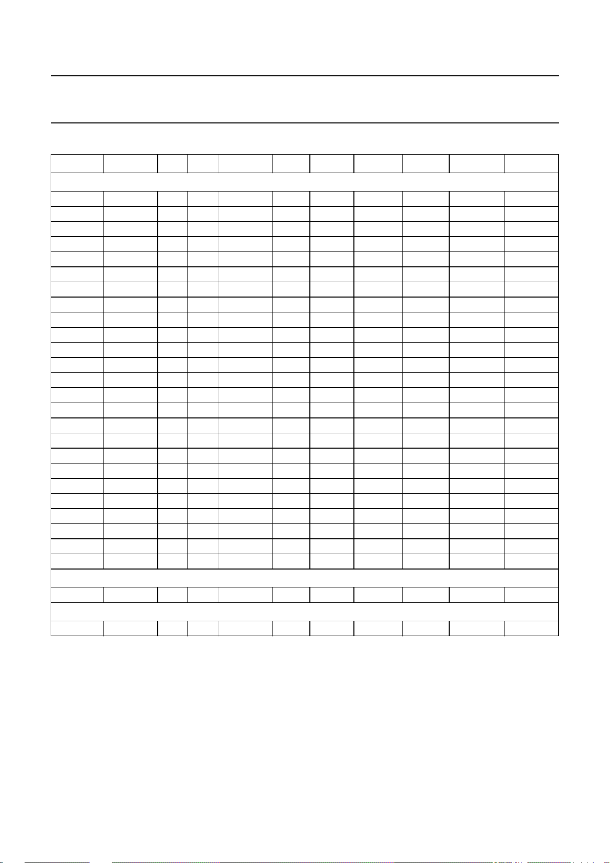
Table 6 Y scaler programming at NTSC, input frame size: 640 × 400, full anti-flicker filter
TV LINE OFFSET FAL LAL PCL YINC YSKIP YOFSO YOFSE YIWGTO YIWGTE
Regular size (horizontal TV size: 640 pixels, offset ±10 pixels)
212 −4 29 241 1851099 2163 0 52 52 3128 1080
212 −2 31 243 1851099 2163 0 56 56 3128 1080
212 0 33 245 1851099 2163 0 60 60 3128 1080
212 2 35 247 1851099 2163 0 63 63 3128 1080
212 4 37 249 1851099 2163 0 67 67 3128 1080
214 −4 28 242 1836201 2181 0 50 50 3138 1090
214 −2 30 244 1836201 2181 0 54 54 3138 1090
214 0 32 246 1836201 2181 0 57 57 3138 1090
214 2 34 248 1836201 2181 0 61 61 3138 1090
214 4 36 250 1836201 2181 0 65 65 3138 1090
216 −4 27 243 1817578 2202 0 47 47 3148 1100
216 −2 29 245 1817578 2202 0 51 51 3148 1100
216 0 31 247 1817578 2202 0 55 55 3148 1100
216 2 33 249 1817578 2202 0 58 58 3148 1100
216 4 35 251 1817578 2202 0 62 62 3148 1100
218 −4 26 244 1802680 2222 0 45 45 3158 1110
218 −2 28 246 1802680 2222 0 49 49 3158 1110
218 0 30 248 1802680 2222 0 53 53 3158 1110
218 2 32 250 1802680 2222 0 56 56 3158 1110
218 4 34 252 1802680 2222 0 60 60 3158 1110
220 −4 25 245 1784057 2245 0 43 43 3168 1120
220 −2 27 247 1784057 2245 0 46 46 3168 1120
220 0 29 249 1784057 2245 0 50 50 3168 1120
220 2 31 251 1784057 2245 0 54 54 3168 1120
220 4 33 253 1784057 2245 0 57 57 3168 1120
Overscan (horizontal size: 710 pixels)
241 0 0 0 0 0 0 0 0 0 0
Small size (horizontal size: 620 pixels)
204 0 37 241 1925590 2079 0 70 70 3087 1039
; see Table 23.
2001 Sep 25 17

Philips Semiconductors Product specification
Digital video encoder SAA7102; SAA7103
Table 7 Y scaler programming at NTSC, input frame size: 640 × 400, half anti-flicker filter
TV LINE OFFSET FAL LAL PCL YINC YSKIP YOFSO YOFSE YIWGTO YIWGTE
Regular size (horizontal TV size: 640 pixels, offset ±10 pixels)
212 −4 29 241 1851099 3123 1820 52 52 3668 596
212 −2 31 243 1851099 3123 1820 56 56 3668 596
212 0 33 245 1851099 3123 1820 60 60 3668 596
212 2 35 247 1851099 3123 1820 64 64 3668 596
212 4 37 249 1851099 3123 1820 67 67 3668 596
214 −4 28 242 1836201 3135 1790 50 50 3683 611
214 −2 30 244 1836201 3135 1790 54 54 3683 611
214 0 32 246 1836201 3135 1790 58 58 3683 611
214 2 34 248 1836201 3135 1790 61 61 3683 611
214 4 36 250 1836201 3135 1790 65 65 3683 611
216 −4 27 243 1817578 3145 1750 48 48 3698 626
216 −2 29 245 1817578 3145 1750 51 51 3698 626
216 0 31 247 1817578 3145 1750 55 55 3698 626
216 2 33 249 1817578 3145 1750 59 59 3698 626
216 4 35 251 1817578 3145 1750 63 63 3698 626
218 −4 26 244 1802680 3155 1720 45 45 3714 642
218 −2 28 246 1802680 3155 1720 49 49 3714 642
218 0 30 248 1802680 3155 1720 53 53 3714 642
218 2 32 250 1802680 3155 1720 56 56 3714 642
218 4 34 252 1802680 3155 1720 60 60 3714 642
220 −4 25 245 1784057 3165 1680 43 43 3729 657
220 −2 27 247 1784057 3165 1680 47 47 3729 657
220 0 29 249 1784057 3165 1680 50 50 3729 657
220 2 31 251 1784057 3165 1680 54 54 3729 657
220 4 33 253 1784057 3165 1680 58 58 3729 657
Full size (horizontal size: 710 pixels)
241 0 0 0 0 0 0 0 0 0 0
Small size (horizontal size: 620 pixels)
204 0 37 241 1925590 3087 1980 70 70 3589 551
2001 Sep 25 18

Philips Semiconductors Product specification
Digital video encoder SAA7102; SAA7103
Table 8 Y scaler programming at NTSC, input frame size: 640 × 400, no anti-flicker filter
TV LINE OFFSET FAL LAL PCL YINC YSKIP YOFSO YOFSE YIWGTO YIWGTE
Regular size (horizontal TV size: 640 pixels, offset ±10 pixels)
212 −4 29 241 1851099 4094 3655 52 52 4092 216
212 −2 31 243 1851099 4094 3655 56 56 4092 216
212 0 33 245 1851099 4094 3655 60 60 4092 216
212 2 35 247 1851099 4094 3655 64 64 4092 216
212 4 37 249 1851099 4094 3655 68 68 4092 216
214 −4 28 242 1836201 4090 3580 50 50 4091 253
214 −2 30 244 1836201 4090 3580 54 54 4091 253
214 0 32 246 1836201 4090 3580 58 58 4091 253
214 2 34 248 1836201 4088 3580 61 61 4091 253
214 4 36 250 1836201 4088 3580 65 65 4091 253
216 −4 27 243 1817578 4093 3510 48 48 4091 288
216 −2 29 245 1817578 4093 3510 52 52 4091 288
216 0 31 247 1817578 4093 3510 55 55 4091 288
216 2 33 249 1817578 4093 3510 59 59 4091 288
216 4 35 251 1817578 4093 3510 63 63 4091 288
218 −4 26 244 1802680 4092 3445 46 46 4092 322
218 −2 28 246 1802680 4092 3445 49 49 4092 322
218 0 30 248 1802680 4092 3445 53 53 4092 322
218 2 32 250 1802680 4092 3445 57 57 4092 322
218 4 34 252 1802680 4092 3445 60 60 4092 322
220 −4 25 245 1784057 4090 3370 43 43 4091 358
220 −2 27 247 1784057 4090 3370 47 47 4091 358
220 0 29 249 1784057 4090 3370 50 50 4091 358
220 2 31 251 1784057 4090 3370 54 54 4091 358
220 4 33 253 1784057 4090 3370 58 58 4091 358
Full size (horizontal size: 710 pixels)
241 0 0 0 0 0 0 0 0 0 0
Small size (horizontal size: 620 pixels)
204 0 37 241 1925590 4087 3950 70 70 4089 66
2001 Sep 25 19

Philips Semiconductors Product specification
Digital video encoder SAA7102; SAA7103
Table 9 Y scaler programming at NTSC, input frame size: 640 × 480, full anti-flicker filter
TV LINE OFFSET FAL LAL PCL YINC YSKIP YOFSO YOFSE YIWGTO YIWGTE
Regular size (horizontal TV size: 640 pixels, offset ±10 pixels)
212 −4 29 241 2219829 1804 0 63 63 2948 900
212 −2 31 243 2219829 1804 0 67 67 2948 900
212 0 33 245 2219829 1804 0 72 72 2948 900
212 2 35 247 2219829 1804 0 77 77 2948 900
212 4 37 249 2219829 1804 0 81 81 2948 900
214 −4 28 242 2201206 1819 0 60 60 2957 909
214 −2 30 244 2201206 1819 0 65 65 2957 909
214 0 32 246 2201206 1819 0 69 69 2957 909
214 2 34 248 2201206 1819 0 73 73 2957 909
214 4 36 250 2201206 1819 0 78 78 2957 909
216 −4 27 243 2178859 1836 0 57 57 2965 917
216 −2 29 245 2178859 1836 0 61 61 2965 917
216 0 31 247 2178859 1836 0 66 66 2965 917
216 2 33 249 2178859 1836 0 70 70 2965 917
216 4 35 251 2178859 1836 0 75 75 2965 917
218 −4 26 244 2160236 1853 0 54 54 2974 926
218 −2 28 246 2160236 1853 0 59 59 2974 926
218 0 30 248 2160236 1853 0 63 63 2974 926
218 2 32 250 2160236 1853 0 68 68 2974 926
218 4 34 252 2160236 1853 0 72 72 2974 926
220 −4 25 245 2141613 1870 0 52 52 2982 934
220 −2 27 247 2141613 1870 0 56 56 2982 934
220 0 29 249 2141613 1870 0 61 61 2982 934
220 2 31 251 2141613 1870 0 65 65 2982 934
220 4 33 253 2141613 1870 0 69 69 2982 934
Full size (horizontal size: 710 pixels)
241 0 0 0 0 0 0 0 0 0 0
Small size (horizontal size: 620 pixels)
204 0 37 241 2309218 1734 0 84 84 2941 866
2001 Sep 25 20

Philips Semiconductors Product specification
Digital video encoder SAA7102; SAA7103
Table 10 Y scaler programming at NTSC, input frame size: 640 × 480, half anti-flicker filter
TV LINE OFFSET FAL LAL PCL YINC YSKIP YOFSO YOFSE YIWGTO YIWGTE
Regular size (horizontal TV size: 640 pixels, offset ±10 pixels)
212 −4 29 241 2219829 2704 2048 63 63 3399 327
212 −2 31 243 2219829 2704 2048 67 67 3399 327
212 0 33 245 2219829 2704 2048 72 72 3399 327
212 2 35 247 2219829 2704 2048 77 77 3399 327
212 4 37 249 2219829 2704 2048 81 81 3399 327
214 −4 28 242 2201206 2730 2048 60 60 3412 340
214 −2 30 244 2201206 2730 2048 65 65 3412 340
214 0 32 246 2201206 2730 2048 69 69 3412 340
214 2 34 248 2201206 2730 2048 74 74 3412 340
214 4 36 250 2201206 2730 2048 78 78 3412 340
216 −4 27 243 2178859 2756 2048 57 57 3424 352
216 −2 29 245 2178859 2756 2048 62 62 3424 352
216 0 31 247 2178859 2756 2048 66 66 3424 352
216 2 33 249 2178859 2756 2048 71 71 3424 352
216 4 35 251 2178859 2756 2048 75 75 3424 352
218 −4 26 244 2160236 2781 2048 55 55 3437 365
218 −2 28 246 2160236 2781 2048 59 59 3437 365
218 0 30 248 2160236 2781 2048 63 63 3437 365
218 2 32 250 2160236 2781 2048 68 68 3437 365
218 4 34 252 2160236 2781 2048 72 72 3437 365
220 −4 25 245 2141613 2807 2048 52 52 3450 378
220 −2 27 247 2141613 2807 2048 57 57 3450 378
220 0 29 249 2141613 2807 2048 61 61 3450 378
220 2 31 251 2141613 2807 2048 65 65 3450 378
220 4 33 253 2141613 2807 2048 70 70 3450 378
Full size (horizontal size: 710 pixels)
241 0 0 0 0 0 0 0 0 0 0
Small size (horizontal size: 620 pixels)
204 0 37 241 2309218 2602 2048 84 84 3348 276
2001 Sep 25 21
Philips Semiconductors Product specification
Digital video encoder SAA7102; SAA7103
Table 11 Y scaler programming at NTSC, input frame size: 640 × 480, no anti-flicker filter
TV LINE OFFSET FAL LAL PCL YINC YSKIP YOFSO YOFSE YIWGTO YIWGTE
Regular size (horizontal TV size: 640 pixels, offset ±10 pixels)
212 −4 29 241 2219829 3607 4095 63 64 3849 3362
212 −2 31 243 2219829 3607 4095 68 69 3849 3362
212 0 33 245 2219829 3607 4095 72 73 3849 3362
212 2 35 247 2219829 3607 4095 77 78 3849 3362
212 4 37 249 2219829 3607 4095 81 82 3849 3362
214 −4 28 242 2201206 3639 4095 60 61 3866 3413
214 −2 30 244 2201206 3639 4095 65 66 3866 3413
214 0 32 246 2201206 3639 4095 69 70 3866 3413
214 2 34 248 2201206 3639 4095 74 75 3866 3413
214 4 36 250 2201206 3639 4095 78 79 3866 3413
216 −4 27 243 2178859 3675 4095 57 58 3883 3464
216 −2 29 245 2178859 3675 4095 62 63 3883 3464
216 0 31 247 2178859 3675 4095 66 67 3883 3464
216 2 33 249 2178859 3675 4095 71 72 3883 3464
216 4 35 251 2178859 3675 4095 75 76 3883 3464
218 −4 26 244 2160236 3709 4095 55 56 3900 3515
218 −2 28 246 2160236 3709 4095 59 60 3900 3515
218 0 30 248 2160236 3709 4095 64 65 3900 3515
218 2 32 250 2160236 3709 4095 68 69 3900 3515
218 4 34 252 2160236 3709 4095 73 74 3900 3515
220 −4 25 245 2141613 3741 4095 52 53 3917 3566
220 −2 27 247 2141613 3741 4095 57 58 3917 3566
220 0 29 249 2141613 3741 4095 61 62 3917 3566
220 2 31 251 2141613 3741 4095 65 66 3917 3566
220 4 33 253 2141613 3741 4095 70 71 3917 3566
Full size (horizontal size: 710 pixels)
241 0 0 0 0 0 0 0 0 0 0
Small size (horizontal size: 620 pixels)
204 0 37 241 2309218 3471 4095 85 86 3781 3158
2001 Sep 25 22

Philips Semiconductors Product specification
Digital video encoder SAA7102; SAA7103
Table 12 Y scaler programming at NTSC, input frame size: 800 × 600, full anti-flicker filter
TV LINE OFFSET FAL LAL PCL YINC YSKIP YOFSO YOFSE YIWGTO YIWGTE
Regular size (horizontal TV size: 640 pixels, offset ±10 pixels)
212 −4 29 241 3551726 1443 0 79 79 2769 721
212 −2 31 243 3551726 1443 0 84 84 2769 721
212 0 33 245 3551726 1443 0 90 90 2769 721
212 2 35 247 3551726 1443 0 96 96 2769 721
212 4 37 249 3551726 1443 0 102 102 2769 721
214 −4 28 242 3518354 1457 0 75 75 2776 728
214 −2 30 244 3518354 1457 0 81 81 2776 728
214 0 32 246 3518354 1457 0 86 86 2776 728
214 2 34 248 3518354 1457 0 92 92 2776 728
214 4 36 250 3518354 1457 0 98 98 2776 728
216 −4 27 243 3484982 1470 0 72 72 2782 734
216 −2 29 245 3484982 1470 0 77 77 2782 734
216 0 31 247 3484982 1470 0 82 82 2782 734
216 2 33 249 3484982 1470 0 88 88 2782 734
216 4 35 251 3484982 1470 0 94 94 2782 734
218 −4 26 244 3451610 1484 0 68 68 2789 741
218 −2 28 246 3451610 1484 0 73 73 2789 741
218 0 30 248 3451610 1484 0 79 79 2789 741
218 2 32 250 3451610 1484 0 85 85 2789 741
218 4 34 252 3451610 1484 0 90 90 2789 741
220 −4 25 245 3423006 1497 0 65 65 2796 748
220 −2 27 247 3423006 1497 0 71 71 2796 748
220 0 29 249 3423006 1497 0 76 76 2796 748
220 2 31 251 3423006 1497 0 81 81 2796 748
220 4 33 253 3423006 1497 0 87 87 2796 748
Full size (horizontal size: 710 pixels)
241 0 18 259 3122659 1642 0 42 42 2867 819
Small size (horizontal size: 620 pixels)
204 0 37 241 3689981 1389 0 106 106 2742 694
2001 Sep 25 23
 Loading...