

Philips SAA6721E Datasheet
INTEGRATED CIRCUITS
DATA SH EET
SAA6721E
SXGA RGB to TFT graphics engine
Preliminary specification
File under Integrated Circuits, IC02
1999 May 11

Philips Semiconductors Preliminary specification
SXGA RGB to TFT graphics engine SAA6721E
CONTENTS
1 FEATURES
1.1 RGB video input
1.2 YUV video input
1.3 Video processing
1.4 On screen display
1.5 Video output
1.6 Memory interface
1.7 Miscellaneous
2 GENERAL DESCRIPTION
3 QUICK REFERENCE DATA
4 ORDERING INFORMATION
5 BLOCK DIAGRAM
6 PINNING INFORMATION
7 FUNCTIONAL DESCRIPTION
7.1 Data path
7.2 System clocks
7.2.1 Input interface clock (VCLK)
7.2.2 Memory interface clock (MCLKI)
7.2.3 I2C-bus interface clock (SCL)
7.2.4 System clock (CLK)
7.2.5 TFT panel clock (PCLK)
7.3 RGB input port
7.4 YUV input port
7.5 TFT output port
7.5.1 Single pixel mode
7.5.2 Double pixel mode
7.6 Memory port
7.6.1 SDRAM memory configuration
7.6.2 SGRAM memory configuration
7.7 I2C-bus interface
7.8 De-interlacing algorithms
7.8.1 Static mesh mode
7.8.2 Spatial filtering
7.8.3 Temporal filtering
7.9 Scaling algorithm
7.9.1 Upscaling
7.9.2 Downscaling
8 SYSTEM DESCRIPTION
8.1 Programming registers
8.2 Clock management
8.2.1 Clock generation and multiplexing
8.2.2 Clock divider
8.3 RGB/YUV input interface
8.3.1 Sampling mode
8.3.2 RGB data sampling
8.3.3 Clamp pulse generation
8.3.4 Gain correction pulse generation
8.3.5 YUV data sampling
8.4 Video mode and synchronization signal
detection
8.5 Memory interface and de-interlacer unit
8.5.1 Memory interface limitations
8.5.2 Initialization of external memory
8.5.3 Frame and field memory
8.5.4 Frame recovery
8.6 Scaling
8.6.1 Downscaling
8.6.2 Upscaling
8.6.3 Upscaler transition function
8.7 Panning unit
8.8 Overlay port
8.8.1 Overlay insertion
8.8.2 Sync generation
8.8.3 Data sampling
8.8.4 OVCLK gating
8.9 Colour space matrix
8.10 Colour correction
8.11 On screen display
8.11.1 OSD generals
8.11.2 OSD window
8.11.3 OSD character matrix
8.12 Temporal dithering (frame rate controller)
8.13 Output interface
8.13.1 General
8.13.2 Frame generation
8.13.3 Timing reference signals
9 LIMITING VALUES
10 CHARACTERISTICS
11 TIMING CHARACTERISTICS
12 APPLICATION INFORMATION
13 PACKAGE OUTLINE
14 SOLDERING
14.1 Introduction to soldering surface mount
packages
14.2 Reflow soldering
14.3 Wave soldering
14.4 Manual soldering
14.5 Suitability of surface mount IC packages for
wave and reflow soldering methods
15 DEFINITIONS
16 LIFE SUPPORT APPLICATIONS
17 PURCHASE OF PHILIPS I2C COMPONENTS
1999 May 11 2

Philips Semiconductors Preliminary specification
SXGA RGB to TFT graphics engine SAA6721E
1 FEATURES
1.1 RGB video input
• Digital single (24-bit) or dual (48-bit) channel RGB input
• Data input of sampled RGB data with a pixel frequency
of maximum 150 MHz
• Free definable data acquisition offsets and vertical
window size in single pixel increments, horizontal
window size in double pixel increments
• Programmable pulses for ADC clamping and ADC gain
correction
• Detection of presence of sync signals, and of their
polarities
• Support for auto-adjustment functions for sample clock
frequency, phase, vertical and horizontal sample offset,
as well as colour adjustment
• Maximum supported resolution of 1280 × 1024 dots
Super Extended Graphics Adapter (SXGA)
• Support for detection of the applied graphics mode
(multi-sync).
1.2 YUV video input
• Pin sharing between YUV and RGB input port
• YUV 4 : 4 : 4, YUV 4 : 2 : 2, YUV 4 : 2 : 2 with CCIR 656
codes, YUV 4:1:1 input of interlaced and
non-interlaced digital video data
• Maximum picture resolution of 1024 × 1024 pixels for
interlaced or non-interlaced video
• Input of video data at maximum 75 MHz
• Free definable data acquisition offsets and window in
double pixel or single line increments
• YUV to RGB colour space conversion.
1.3 Video processing
• Colour correction Look-Up Table (LUT)
• Phase correct up and downscaling of the RGB data
• Fully programmable scaling ratios
• Independent horizontal and vertical scaling engine
• Free definable position of the scaled input picture inside
the output picture with programmable border colour
• De-interlacing unit for digital YUV video data
• Zoom up to full-screen resolution of the de-interlaced
YUV video stream via the main scaler.
1.4 On screen display
• Character based internal On Screen Display (OSD)
• Programmable character matrix sizes of either
24 × 24 pixels (42 characters available) or
12 × 16 pixels (128 characters available)
• Programmable width and height of the OSD window,
built from maximum 1152 characters
• 8 different colours for foreground and background
inclusive transparent colours
• Overlay port for external OSD controller.
1.5 Video output
• Single pixel/clock (24-bit) or double pixel/clock (48-bit)
digital RGB output
• Generation of synchronization and validation signals for
the Thin Film Transistor (TFT) display
• Frame rate control (temporal dithering) for displaying
true colour graphics on high colour displays
• Free programmable timing for displays of several
manufacturers.
1.6 Memory interface
• Support of both 1M × 16 SDRAM,256k × 32 SGRAM or
128k × 32 SGRAM devices
• Maximum memory clock frequency of 125 MHz
• Scalable memory size built of either 2, 3 or 4 SDRAM,
or of 1 or 2 SGRAM devices
• Special mode for operation without external memory.
1.7 Miscellaneous
• Internal Phase-Locked Loop (PLL) for memory and
panel clock generation from the system clock
2
C-bus interface with 2 selectable addresses
• I
• Boundary scan test circuit and Joint Test Action Group
(JTAG) test controller.
1999 May 11 3
Philips Semiconductors Preliminary specification
SXGA RGB to TFT graphics engine SAA6721E
2 GENERAL DESCRIPTION
The SAA6721E is a graphics engine, which converts
digital RGB or YUV data into video signals suitable for TFT
displays. It supports SXGA input resolution as well as true
colour. Independent horizontal and vertical up and
downscaling can display the input data arbitrarily on the
connected TFT display. Multi-sync capability allows the
applied graphics mode to be detected.
Overlay signals can be generated either by an internal
The SAA6721E must be embedded into a system
containing a microcontroller with an I
2
C-bus serial
interface. For multi-sync capabilities a frame buffer built
from SGRAM or SDRAM is needed. The size of this frame
buffer depends on the maximum resolution and bandwidth
needed for the application. For converting the analog RGB
stream into a digital data stream one or two ADCs with
3 channels each for R, G and B are needed. If the YUV
input is used, a video front-end chip such as the SAA7113
must be used in front of the YUV port.
OSD generator or supplied via the overlay port from an
external OSD controller.
3 QUICK REFERENCE DATA
SYMBOL PARAMETER MIN. TYP. MAX. UNIT
V
I
DDD
V
V
DDD
i
o
digital supply voltage 3.0 3.3 3.6 V
digital supply current − 600 840 mA
input voltages LVTTL compatible
output voltages memory port LVTTL compatible
output voltages TFT port CMOS compatible
T
amb
ambient temperature 0 − 70 °C
4 ORDERING INFORMATION
PACKAGE
TYPE NUMBER
NAME DESCRIPTION VERSION
SAA6721E BGA292 plastic ball grid array package; 292 balls; body 27 × 27 × 1.75 mm SOT489-1
1999 May 11 4

This text is here in white to force landscape pages to be rotated correctly when browsing through the pdf in the Acrobat reader.This text is here in
h
_white to force landscape pages to be rotated correctly when browsing through the pdf in the Acrobat reader.This text is here inThis text is here in
white to force landscape pages to be rotated correctly when browsing through the pdf in the Acrobat reader. white to force landscape pages to be ...
1999 May 11 5
andbook, full pagewidth
5 BLOCK DIAGRAM
SXGA RGB to TFT graphics engine SAA6721E
Philips Semiconductors Preliminary specification
VCLK
VVS
VHS
CLAMP
GAINC
VPA7 to VPA0
VPB7 to VPB0
VPC7 to VPC0
VPD7 to VPD0
VPE7 to VPE0
VPF7 to VPF0
MCLKI
CLK
MODE/SYNC
DETECTION
RGB/YUV
INPUT
INTERFACE
PLL
RGB
raw data
RGB/YUV
÷2
DIVIDER
input frame size and
sync information
AUTO
ADJUSTMENT
CONTROLLER
data
DOWN
SCALER
memory
clock
panel
clock
frequency,
phase and
colour
information
LINE MEMORY
YUV
RGB
SDA
SCL
SAD
I2C-BUS
INTERFACE
GLOBAL CONTROL
UNIT
UP
SCALER
SAA6721E
MEMORY INTERFACE
DE-INTERLACER
INT TDO
RST
COLOUR
CORRECTION
ON
SCREEN
DISPLAY
TMS TCLK
TDI
TRST
JTAG
CONTROLLER
PANNING
UNIT
TEMPORAL
DITHERING
OVA2 to OVA0
OVB2
OVACT
OVB0
OVERLAY
OVVS
OVHS
to
OSD
PORT
OUTPUT
INTERFACE
OVCLK
PAR7 to PAR0
PAG7 to PAG0
PAB7 to PAB0
PBR7 to PBR0
PBG7 to PBG0
PBB7 to PBB0
PVS
PHS
PDE
PCLK
DQ63
to
DQ0
BA
DQM
A10
RAS CAS WE
to
A0
Fig.1 Block diagram.
MCLKO
V
SSDVDDD
V
SS(PLL)
V
DD(PLL)
MHB241
Philips Semiconductors Preliminary specification
SXGA RGB to TFT graphics engine SAA6721E
6 PINNING INFORMATION
handbook, halfpage
Y
W
V
U
T
R
P
N
M
L
K
J
H
G
F
E
D
C
B
A
SAA6721E
2468101214161820
135791113151719
MHB242
Fig.2 Pin configuration.
Table 1
SYMBOL PIN PORT I/O
(1)
DESCRIPTION
VCLK N1 RGB/YUV input input RGB/YUV sample clock
VVS M3 RGB/YUV input input RGB/YUV vertical sync
VHS M2 RGB/YUV input input RGB/YUV horizontal sync
VPA7 C7 RGB/YUV input input video input port A;
VPA6 A6 RGB/YUV input input
RGB port 0 red channel or YUV port luminance
VPA5 B6 RGB/YUV input input
VPA4 C6 RGB/YUV input input
VPA3 A5 RGB/YUV input input
VPA2 D5 RGB/YUV input input
VPA1 B5 RGB/YUV input input
VPA0 C5 RGB/YUV input input
1999 May 11 6
Philips Semiconductors Preliminary specification
SXGA RGB to TFT graphics engine SAA6721E
SYMBOL PIN PORT I/O
VPB7 A4 RGB/YUV input input video input port B;
VPB6 B4 RGB/YUV input input
VPB5 C4 RGB/YUV input input
VPB4 A3 RGB/YUV input input
VPB3 B3 RGB/YUV input input
VPB2 C3 RGB/YUV input input
VPB1 A2 RGB/YUV input input
VPB0 B2 RGB/YUV input input
VPC7 B1 RGB/YUV input input video input port C;
VPC6 C2 RGB/YUV input input
VPC5 C1 RGB/YUV input input
VPC4 D3 RGB/YUV input input
VPC3 D2 RGB/YUV input input
VPC2 D1 RGB/YUV input input
VPC1 E3 RGB/YUV input input
VPC0 E2 RGB/YUV input input
VPD7 E4 RGB/YUV input input video input port D;
VPD6 E1 RGB/YUV input input
VPD5 F3 RGB/YUV input input
VPD4 F2 RGB/YUV input input
VPD3 F1 RGB/YUV input input
VPD2 G3 RGB/YUV input input
VPD1 G2 RGB/YUV input input
VPD0 G4 RGB/YUV input input
VPE7 G1 RGB/YUV input input video input port E; RGB port 1 green channel
VPE6 H3 RGB/YUV input input
VPE5 H2 RGB/YUV input input
VPE4 H1 RGB/YUV input input
VPE3 J2 RGB/YUV input input
VPE2 J4 RGB/YUV input input
VPE1 J1 RGB/YUV input input
VPE0 K3 RGB/YUV input input
VPF7 K2 RGB/YUV input input video input port F; RGB port 1 blue channel
VPF6 K1 RGB/YUV input input
VPF5 L1 RGB/YUV input input
VPF4 L4 RGB/YUV input input
VPF3 L2 RGB/YUV input input
VPF2 L3 RGB/YUV input input
VPF1 M1 RGB/YUV input input
VPF0 M4 RGB/YUV input input
(1)
DESCRIPTION
RGB port 0 green channel or YUV port chrominance
RGB port 0 blue channel or YUV port chrominance
RGB port 1 red channel or YUV data qualifier port
(VPD7 = CREF clock gating signal;
VPD6 = HREF active horizontal video)
1999 May 11 7
Philips Semiconductors Preliminary specification
SXGA RGB to TFT graphics engine SAA6721E
SYMBOL PIN PORT I/O
CLAMP N2 RGB/YUV input output clamp pulse for analog-to-digital converter
GAINC N3 RGB/YUV input output gain correction pulse for analog-to-digital converter
PCLK Y13 panel interface output panel clock
PVS V12 panel interface output panel vertical sync
PHS W12 panel interface output panel horizontal sync
PDE U12 panel interface output panel data enable
PAR7 P1 panel interface output panel port A red channel
PAR6 P4 panel interface output
PAR5 P2 panel interface output
PAR4 P3 panel interface output
PAR3 R1 panel interface output
PAR2 R2 panel interface output
PAR1 R3 panel interface output
PAR0 T1 panel interface output
PAG7 T4 panel interface output panel port A green channel
PAG6 T2 panel interface output
PAG5 T3 panel interface output
PAG4 U1 panel interface output
PAG3 U2 panel interface output
PAG2 V1 panel interface output
PAG1 V2 panel interface output
PAG0 W1 panel interface output
PAB7 Y1 panel interface output panel port A blue channel
PAB6 W2 panel interface output
PAB5 Y2 panel interface output
PAB4 V3 panel interface output
PAB3 W3 panel interface output
PAB2 Y3 panel interface output
PAB1 V4 panel interface output
PAB0 Y4 panel interface output
PBR7 V5 panel interface output panel port B red channel
PBR6 W5 panel interface output
PBR5 Y5 panel interface output
PBR4 V6 panel interface output
PBR3 W6 panel interface output
PBR2 Y6 panel interface output
PBR1 V7 panel interface output
PBR0 W7 panel interface output
(1)
DESCRIPTION
1999 May 11 8

Philips Semiconductors Preliminary specification
SXGA RGB to TFT graphics engine SAA6721E
SYMBOL PIN PORT I/O
(1)
DESCRIPTION
PBG7 Y7 panel interface output panel port B green channel
PBG6 V8 panel interface output
PBG5 W8 panel interface output
PBG4 Y8 panel interface output
PBG3 V9 panel interface output
PBG2 W9 panel interface output
PBG1 U9 panel interface output
PBG0 Y9 panel interface output
PBB7 V10 panel interface output panel port B blue channel
PBB6 W10 panel interface output
PBB5 Y10 panel interface output
PBB4 Y11 panel interface output
PBB3 U11 panel interface output
PBB2 W11 panel interface output
PBB1 V11 panel interface output
PBB0 Y12 panel interface output
SCL V18 I
SDA W18 input/output I
SAD Y17 input I
2
C-bus interface input I2C-bus interface clock line
2
C-bus interface data line
2
C-bus address select: 0 = 74H, 1 = 76H
OVCLK Y16 overlay output overlay port clock
OVVS W16 overlay output overlay port vertical sync
OVHS V15 overlay output overlay port horizontal sync
OVACT V16 overlay input overlay port pixel active
OVA0 Y14 overlay input overlay port input pixel A
OVA1 V13 overlay input
OVA2 W13 overlay input
OVB0 Y15 overlay input overlay port input pixel B
OVB1 V14 overlay input
OVB2 W14 overlay input
MCLKO A17 memory interface output memory clock output
RAS A18 memory interface output memory Row Address Strobe (RAS) signal (active LOW)
CAS
memory interface output memory Column Address Strobe (CAS) signal
C17
(active LOW)
WE D16 memory interface output memory Write Enable (WE) signal (active LOW)
DQM T17 memory interface output memory data mask (active LOW)
1999 May 11 9

Philips Semiconductors Preliminary specification
SXGA RGB to TFT graphics engine SAA6721E
SYMBOL PIN PORT I/O
A0 A20 memory interface output memory address bus
A1 C20 memory interface output
A2 D20 memory interface output
A3 E19 memory interface output
A4 F18 memory interface output
A5 E17 memory interface output
A6 E18 memory interface output
A7 C19 memory interface output
A8 C18 memory interface output
A9 D18 memory interface output
A10 B19 memory interface output
BA A19 memory interface output memory bank select
DQ0 M20 memory interface input/output memory data bus
DQ1 M19 memory interface input/output
DQ2 N20 memory interface input/output
DQ3 N19 memory interface input/output
DQ4 P19 memory interface input/output
DQ5 R19 memory interface input/output
DQ6 T20 memory interface input/output
DQ7 T19 memory interface input/output
DQ8 T18 memory interface input/output
DQ9 R18 memory interface input/output
DQ10 P18 memory interface input/output
DQ11 P17 memory interface input/output
DQ12 N18 memory interface input/output
DQ13 M18 memory interface input/output
DQ14 M17 memory interface input/output
DQ15 L19 memory interface input/output
DQ16 E20 memory interface input/output
DQ17 F20 memory interface input/output
DQ18 G20 memory interface input/output
DQ19 H20 memory interface input/output
DQ20 J20 memory interface input/output
DQ21 K19 memory interface input/output
DQ22 K20 memory interface input/output
DQ23 L20 memory interface input/output
DQ24 K17 memory interface input/output
DQ25 K18 memory interface input/output
DQ26 J19 memory interface input/output
DQ27 J18 memory interface input/output
DQ28 H19 memory interface input/output
(1)
DESCRIPTION
1999 May 11 10
Philips Semiconductors Preliminary specification
SXGA RGB to TFT graphics engine SAA6721E
SYMBOL PIN PORT I/O
DQ29 H18 memory interface input/output memory data bus
DQ30 G18 memory interface input/output
DQ31 F19 memory interface input/output
DQ32 A12 memory interface input/output
DQ33 B12 memory interface input/output
DQ34 A13 memory interface input/output
DQ35 B13 memory interface input/output
DQ36 A14 memory interface input/output
DQ37 B14 memory interface input/output
DQ38 A15 memory interface input/output
DQ39 B15 memory interface input/output
DQ40 A16 memory interface input/output
DQ41 C15 memory interface input/output
DQ42 C14 memory interface input/output
DQ43 D14 memory interface input/output
DQ44 C13 memory interface input/output
DQ45 C12 memory interface input/output
DQ46 D12 memory interface input/output
DQ47 C11 memory interface input/output
DQ48 B7 memory interface input/output
DQ49 A7 memory interface input/output
DQ50 B8 memory interface input/output
DQ51 A8 memory interface input/output
DQ52 B9 memory interface input/output
DQ53 A9 memory interface input/output
DQ54 B10 memory interface input/output
DQ55 A10 memory interface input/output
DQ56 B11 memory interface input/output
DQ57 A11 memory interface input/output
DQ58 D10 memory interface input/output
DQ59 C10 memory interface input/output
DQ60 D9 memory interface input/output
DQ61 C9 memory interface input/output
DQ62 C8 memory interface input/output
DQ63 D7 memory interface input/output
TCLK U19 JTAG test controller input JTAG test controller clock; note 2
TRST W17 input JTAG test controller reset (active LOW); note 2
TDI U18 input JTAG test data input; note2
TMS V19 input JTAG test mode select; note 2
TDO W19 output JTAG test data output
(1)
DESCRIPTION
1999 May 11 11
Philips Semiconductors Preliminary specification
SXGA RGB to TFT graphics engine SAA6721E
SYMBOL PIN PORT I/O
(1)
DESCRIPTION
CLK Y19 miscellaneous input system and panel clock
RST Y20 input system reset (active LOW)
INT Y18 output mode detection interrupt (active LOW)
MCLKI W20 input memory clock input
V
SSD
A1 −−digital ground supply
D4
D8
D13
D17
H4
H17
N4
N17
U4
U8
U13
U17
V
DDD
D6 −−digital supply voltage
D11
D15
F4
F17
K4
L17
R4
R17
U6
U10
U15
V
SS(PLL)
V
DD(PLL)
V17 −−ground supply for internal PLL circuitry
U16 −−supply voltage for internal PLL circuitry
n.c. B16 −−not connected
n.c. B17 −−not connected
n.c. B18 −−not connected
n.c. B20 −−not connected
n.c. C16 −−not connected
n.c. D19 −−not connected
n.c. G17 −−not connected
n.c. G19 −−not connected
n.c. J3 −−not connected
n.c. J17 −−not connected
1999 May 11 12
Philips Semiconductors Preliminary specification
SXGA RGB to TFT graphics engine SAA6721E
SYMBOL PIN PORT I/O
(1)
DESCRIPTION
n.c. L18 −−not connected
n.c. P20 −−not connected
n.c. R20 −−not connected
n.c. U3 −−not connected
n.c. U5 −−not connected
n.c. U7 −−not connected
n.c. U14 −−not connected
n.c. U20 −−not connected
n.c. V20 −−not connected
n.c. W4 −−not connected
n.c. W15 −−not connected
Notes
1. Generally all inputs are 5 V tolerant TTL inputs. All outputs are CMOS, except the memory interface ports, which are
LVTTL compatible.
2. Connect to ground when not using the JTAG controller.
7 FUNCTIONAL DESCRIPTION
7.1 Data path
Input video data is sampled either as RGB data in single
pixels from only one ADC or in double pixels in interleaved
format from two ADCs. Alternatively the input interface can
sample interlaced or non-interlaced YUV data. The clock
for sampling the data will always be provided from external
circuitry. The video stream will be adapted from the input
frame rate to the output frame rate needed by the panel.
Therefore a frame buffer built of SDRAMs or SGRAMs is
used. If the panel supports the incoming frame rate from
the RGB port, the adaption can be done without external
memory. If the video stream is in interlaced format the
memory interface activates its de-interlacing unit.
If zooming must be performed the upscaler behind the
memory interface will be enabled. For downscaling the
downscaler in front of the memory interface in the data
path will be used. A colour correction can be done via a
look-up table. The resulting video stream can now be
positioned elsewhere in the output data stream by the
panning unit. If an external OSD controller is embedded
into the system, its OSD window will be put into the video
stream by the OSD overlay port. Additionally the internal
OSD will be inserted in the next stage. The temporal
dithering allows true colour pictures to be displayed on
high colour panels. The output interface provides the
timing and control signals necessary for the connected
panel.
7.2 System clocks
7.2.1 I
NPUT INTERFACE CLOCK (VCLK)
This clock is used for sampling the incoming RGB or YUV
data stream. In RGB mode this clock varies from
25 to 150 MHz in single ADC mode. If two ADCs are used
the RGB input clock is between 12.5 and 75 MHz. In YUV
mode the clock lies in the range of approximately 30 MHz.
The clocks are generated from external devices.
The RGB clock can be generated by the external ADCs or
an external video PLL. The YUV clock must be generated
by the video decoder which also provides the YUV video
data.
7.2.2 M
EMORY INTERFACE CLOCK (MCLKI)
The memory clock is the synchronous clock for the
external frame buffer. Depending on the bandwidth
needed by the application, and the connected SDRAM or
SGRAM devices, the clock varies from 83 to 125 MHz.
It can be generated internally by the PLL from the system
clock (CLK), or by an external quartz oscillator.
If the internal PLL is used, the memory clock frequency
can be derived from the following formula:
f_memory
f_system
----------------------- N
16×=
Where N = pre-divider ratio and f_system = clock at
pin CLK.
1999 May 11 13
Philips Semiconductors Preliminary specification
SXGA RGB to TFT graphics engine SAA6721E
7.2.3 I2C-BUS INTERFACE CLOCK (SCL)
This clock drives the interface to the external
microcontroller. Its frequency range is from
100 kHz to 1 MHz.
7.2.4 S
YSTEM CLOCK (CLK)
This clock is used to drive the internal PLL. The frequency
range is from 24 to 50 MHz.
7.2.5 TFT
PANEL CLOCK (PCLK)
This clock is the timing reference for the panel.
The frequency is the same as the system clock, or it can
be generated from the internal PLL by using the following
formula:
f_tft
f_system
----------------------- N
32
×=
-----M
Where N = pre-divider ratio and M = post-divider ratio.
7.3 RGB input port
The RGB input port can operate in two modes; single pixel
mode (24 bits) and double pixel mode (48 bits). For single
pixel mode only ports VPA7 to VPA0, VPB7 to VPB0, and
VPC7 to VPC0 are internally sampled. For double pixel
mode two pixels must be provided at the RGB input port.
Therefore ports VPD7 to VPD0, VPE7 to VPE0, and
VPF7 to VPF0 are also needed.
The VPA/B/C ports are sampled on the rising edge of the
RGB input clock (VCLK), and the VPD/E/F ports on the
falling edge (see Fig.3).
The synchronization pulses from the graphics card are
used to identify the frame outline. The vertical
synchronization pulse is connected to pin VVS, and the
horizontal synchronization pulse is connected to pin VHS.
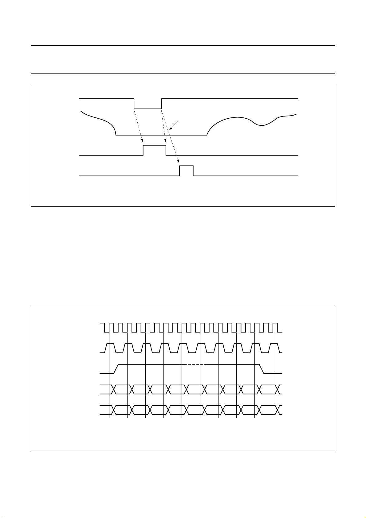
For calibrating the connected Analog-to-Digital Converter
(ADC) the SAA6721E delivers a clamp pulse at
pin CLAMP, and a gain correction pulse at pin GAINC
(see Fig.4).
The sample window of the RGB input port is controlled by
four counters; horizontal and vertical offset, and horizontal
and vertical window size.
The offset counters start at the inactive or second edge of
their corresponding synchronization signal.
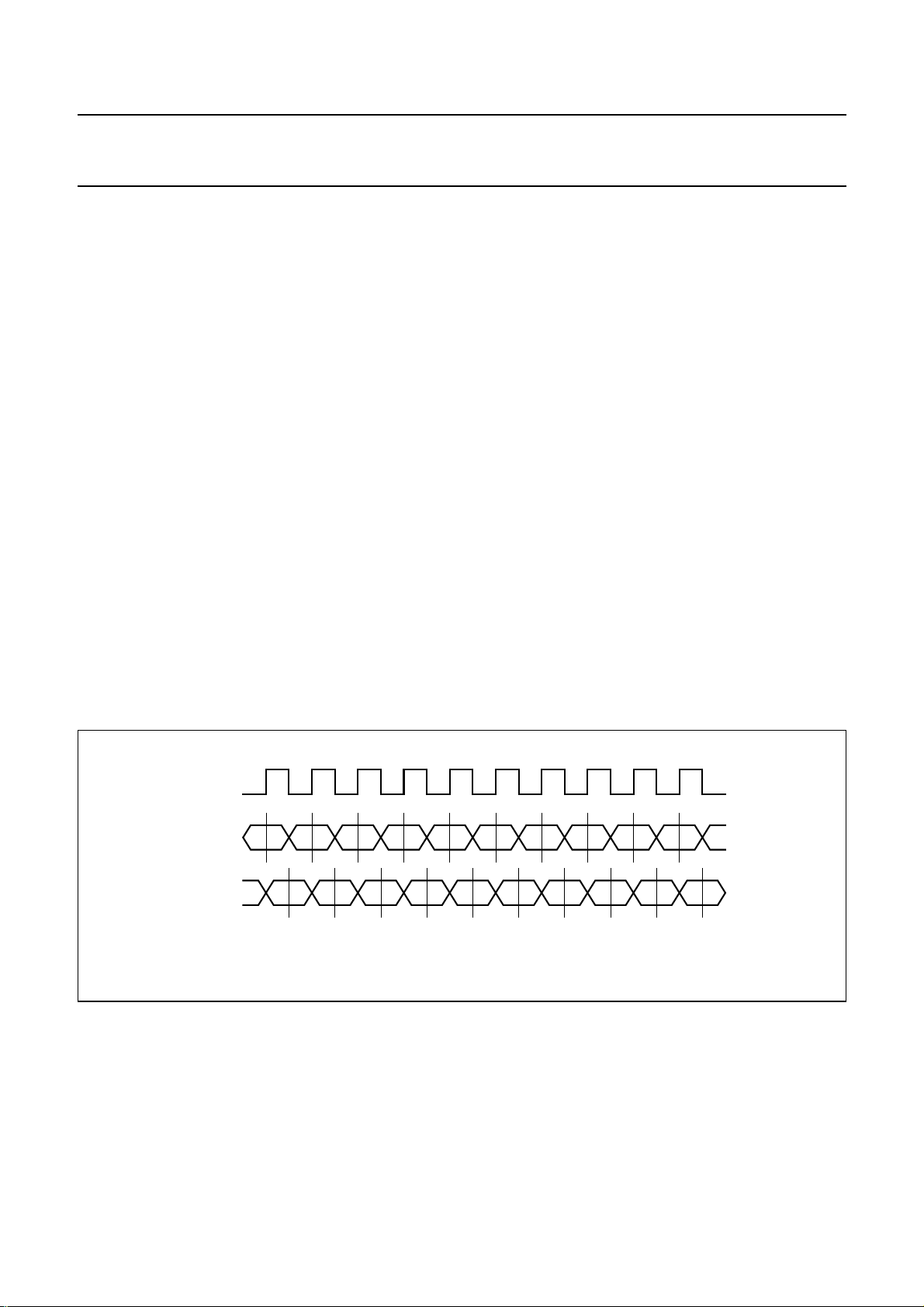
handbook, full pagewidth
VCLK
VPA/B/C
VPD/E/F
Fig.3 RGB input port timing.
1999 May 11 14
MHB243
Philips Semiconductors Preliminary specification
SXGA RGB to TFT graphics engine SAA6721E
handbook, full pagewidth
VHS
RGB data
GAINC
CLAMP
Fig.4 Clamp and gain correction pulses.
7.4 YUV input port
The YUV input port supports interlaced video streams and
provides an easy connection to most common decoder
ICs. It consists of the luminance port VPA7 to VPA0, the
chrominance port VPB7 to VPB0, and eventually
VPC7 to VPC0, which are CCIR 601 level compatible
(Y: 16 to 235, and UV: 16 to 240).
Supported at this port are the formats YUV 4 : 1 : 1,
YUV4:2:2 and YUV 4:2:2 with CCIR 656 codes
(see Table 2).
blanking
MHB244
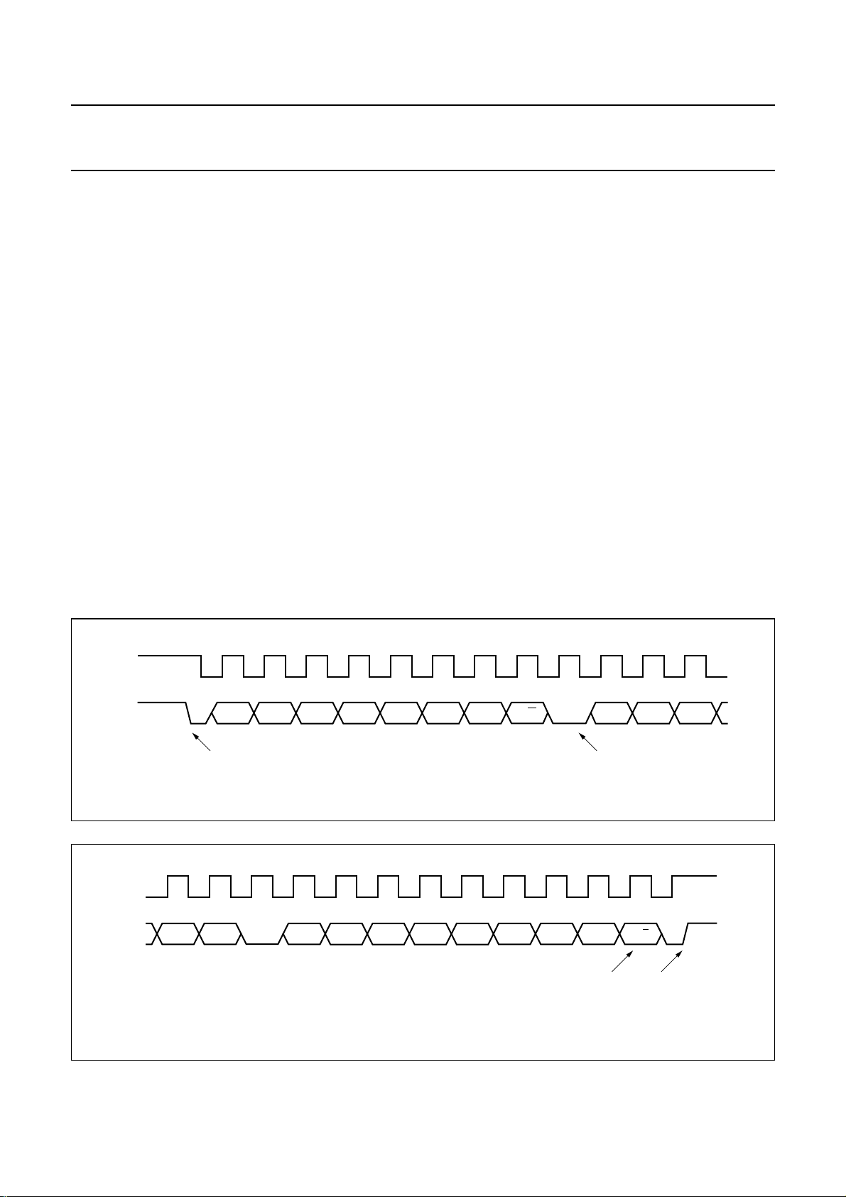
YUV 4:4:4 data can be applied at VPA7 to VPA0 (Y),
VPB7 to VPB0 (U), and VPC7 to VPC0 (V). Input data is
sampled with respect to the clock at pin VCLK if pin VPD7
(CREF) is asserted.
The start of active video data in a line is marked by the
rising edge at pin VPD6 (HREF) and the end of valid video
data is marked by the falling edge at pin VPD6. Figure 5
illustrates this at a YUV 4 :2:2 example.
handbook, full pagewidth
VCLK
CREF
HREF
Y7 to Y0
UV7 to UV0
XX
XX
Y0 XXY719Y6Y5...Y3Y2Y1
U0 XXV718U718V716...V2U2V0
Fig.5 CREF and HREF timing.
1999 May 11 15
MHB245

Philips Semiconductors Preliminary specification
SXGA RGB to TFT graphics engine SAA6721E
Table 2 YUV input formats
SIGNAL 4:1:1 FORMAT 4:2:2 FORMAT CCIR 656
Y7 Y07 Y17 Y27 Y37 Y07 Y17 U07 Y07 V07 Y17
Y6 Y06 Y16 Y26 Y36 Y06 Y16 U06 Y06 V06 Y16
Y5 Y05 Y15 Y25 Y35 Y05 Y15 U05 Y05 V05 Y15
Y4 Y04 Y14 Y24 Y34 Y04 Y14 U04 Y04 V04 Y14
Y3 Y03 Y13 Y23 Y33 Y03 Y13 U03 Y03 V03 Y13
Y2 Y02 Y12 Y22 Y32 Y02 Y12 U02 Y02 V02 Y12
Y1 Y01 Y11 Y21 Y31 Y01 Y11 U01 Y01 V01 Y11
Y0 Y00 Y10 Y20 Y30 Y00 Y10 U00 Y00 V00 Y10
UV7 U07 U05 U03 U01 U07 V07 X X X X
UV6 U06 U04 U02 U00 U06 V06 X X X X
UV5 V07 V05 V03 V01 U05 V05 X X X X
UV4 V06 V04 V02 V00 U04 V04 X X X X
UV3 XXXXU03V03XXXX
UV2 XXXXU02V02XXXX
UV1 XXXXU01V01XXXX
UV0 XXXXU00V00XXXX
Data frequency
1
⁄2VCLK
1
⁄2VCLK VCLK
For YUV 4 :4:4 the Y, U, and V components are available
in parallel.
If non-interlaced video data is applied, it is treated as odd
fields. Interlaced video data is sampled odd field,
even field, odd field, even field, etc. If there are equal
subsequent frames, only the first of these frames will be
handbook, full pagewidth
VCLK
Y7 to Y0
FF ...Y1V0Y0U0SAV0000XX
Fig.6 CCIR 656 SAV code.
handbook, full pagewidth
VCLK
Y7 to Y0
U718 XXEAV0000FFY719V718Y718...
sampled. The decoding of odd and even fields is done with
HREF. In CCIR 656 data streams the included codes are
used for identifying even and odd frames, blanking and
active video data. The codes start with the byte sequence
FF 00 00, followed by the reference code byte;
see Figs 6 and 7.
MHB246
MHB247
Fig.7 CCIR 656 EAV code.
1999 May 11 16
Philips Semiconductors Preliminary specification
SXGA RGB to TFT graphics engine SAA6721E
The CCIR 656 code byte contains vertical and horizontal
blanking as well as odd and even field information, the
protection bits P3 to P0 are ignored.
Table 3 CCIR 656 code byte
MSB LSB
76543210
1F
(2)
V
(3)
H
P3 P2 P1 P0
(1)
Notes
1. F = 0: odd field (field 1); F = 1: even field (field 2).
2. V = 0: in active field lines; V = 1: in field blanking.
3. H = 0: SAV (Start of Active Video);
H = 1: EAV (End of Active Video).
The sample window of the YUV input port is controlled by
four counters; horizontal and vertical offset, and horizontal
and vertical window size. The vertical offset counter starts
counting from the inactive or second edge of its
corresponding reference signal. The horizontal offset
counter starts with the active edge of the HREF signal.
7.5.2 DOUBLE PIXEL MODE
The double pixel mode is used for direct connection of TFT
panels with double pixel input. Both output ports are used.
The first pixel is applied at port A, and the second at port B.
7.6 Memory port
The memory port connects the SAA6721E to the external
frame buffer. This frame memory can be built from either
1M × 16 SDRAM or 256k × 32 SGRAM devices.
Supported are RAM devices with clock frequencies up to
125 MHz. This clock can be provided either by the internal
PLL, or externally be applied to pin MCLKI.
The memory data bus is split into 4 ports:
port 0 (DQ0 to DQ15), port 1 (DQ16 to DQ31),
port 2 (DQ32 to DQ47) and port 3 (DQ48 to DQ63).
To adapt the external memory to the needs of the
application by means of memory size and bandwidth, it is
possible to scale the external memory by using only the
number of subsequent ports needed to build up the frame
buffer and to achieve the memory bandwidth. As a second
step for bandwidth optimization several speed grades of
memory devices can be used.
7.5 TFT output port
The TFT output port consists of two pixel ports (A and B),
each containing red, green and blue colour information
with a resolution of 8 bits per colour. The first pixel port is
mapped to PAR7 to PAR0, PAG7 to PAG0, and
PAB7 to PAB0. The second port is mapped to
PBR7 to PBR0, PBG7 to PBG0, and PBB7 to PBB0.
The vertical and horizontal synchronization signals are
mapped to pins PVS and PHS. A data validation signal
framing visible pixels is available at pin PDE.
All of the above mentioned signals are synchronized to the
output clock at pin PCLK. The active edge of this clock is
programmable.
7.5.1 SINGLE PIXEL MODE
The single pixel mode is designed to support TFT panels
with single pixel input, and for direct connection of panel
link transmitters. Only the first pixel port PAR7 to PAR0,
PAG7 to PAG0, and PAB7 to PAB0 is used. The data is
applied at double the frequency in comparison to the
double pixel output mode.
7.6.1 SDRAM
MEMORY CONFIGURATION
SDRAMs are available in sizes from 16 Mbits. For this
application a wide data bus is required, so that at least
1M × 16 devices must be used. To achieve the desired
bandwidth, 2 to 4 devices must be used in parallel, which
results in a frame buffer size of 4 to 8 Mbytes. But only half
of this memory will be used by the SAA6721E.
The memory port of the SAA6721E can be divided into
4 SDRAM channels. Each channel is 16 bits wide, and
provides in High Speed Channel (HSC) mode with a
125 MHz memory clock and an effective bandwidth of
228 Mbits/s. A Medium Speed Channel (MSC) with a
100 MHz memory clock gives an effective bandwidth of
182 Mbits/s, 91% effective bandwidth assumed.
Table 4 gives the channel configuration for several input
and panel resolutions.
1999 May 11 17

Philips Semiconductors Preliminary specification
SXGA RGB to TFT graphics engine SAA6721E
Table 4 SDRAM channel configurations
INPUT
RESOLUTION
SVGA (800 × 600) XGA (1024 × 768) SXGA (1280 × 1024)
60 Hz 75 Hz 60 Hz 75 Hz 60 Hz 75 Hz
Panel 2 Mbits frame buffer needed 3 Mbits frame buffer needed 4 Mbits frame buffer needed
XGA
SXGA
(1)
(2)
288 Mbits/s
bandwidth;
2 × HSC or
2 × MSC
307 Mbits/s
bandwidth;
2 × HSC or
2 × MSC
319 Mbits/s
bandwidth;
2 × HSC or
2 × MSC
337 Mbits/s
bandwidth;
2 × HSC or
2 × MSC
411 Mbits/s
bandwidth;
2 × HSC or
3 × MSC
435 Mbits/s
bandwidth;
2 × HSC or
3 × MSC
452 Mbits/s
bandwidth;
2 × HSC or
3 × MSC
476 Mbits/s
bandwidth;
3 × HSC or
3 × MSC
475 Mbits/s
bandwidth;
3 × HSC or
3 × MSC
624 Mbits/s
bandwidth;
3 × HSC or
4 × MSC
540 Mbits/s
bandwidth;
3 × HSC or
3 × MSC
705 Mbits/s
bandwidth;
4 × HSC or
4 × MSC
Notes
1. 36 MHz clock frequency.
2. 50 MHz clock frequency.
7.6.2 SGRAM MEMORY CONFIGURATION
SGRAM devices organized to 256k × 32 bits are available,
and feature the wide data bus for high speed applications.
With these devices a frame buffer can be built, without
wasting memory because of bandwidth. In case of
SGRAM usage, the memory data bus of the SAA6721E
Each channel gives, in HSC mode with 125 MHz clock
frequency, an effective bandwidth of 456 Mbits/s; and in
MSC mode, with 100 MHz clock speed, an effective
bandwidth of 364 Mbits/s.
Table 5 gives the channel configuration for several input
and panel resolutions.
can be split into 2 channels of 32 bits each.
Table 5 SGRAM channel configurations
INPUT
RESOLUTION
SVGA (800 × 600) XGA (1024 × 768) SXGA (1280 × 1024)
60 Hz 75 Hz 60 Hz 75 Hz 60 Hz 75 Hz
Panel 2 Mbits frame buffer needed 3 Mbits frame buffer needed 4 Mbits frame buffer needed
(1)
XGA
SXGA
(2)
288 Mbits/s
bandwidth;
1 × HSC or
1 × MSC
307 Mbits/s
bandwidth;
1 × HSC or
1 × MSC
319 Mbits/s
bandwidth;
1 × HSC or
1 × MSC
337 Mbits/s
bandwidth;
1 × HSC or
1 × MSC
411 Mbits/s
bandwidth;
1 × HSC or
2 × MSC
435 Mbits/s
bandwidth;
1 × HSC or
2 × MSC
452 Mbits/s
bandwidth;
1 × HSC or
2 × MSC
476 Mbits/s
bandwidth;
2 × HSC or
2 × MSC
475 Mbits/s
bandwidth;
2 × HSC or
2 × MSC
624 Mbits/s
bandwidth;
2 × HSC or
2 × MSC
540 Mbits/s
bandwidth;
2 × HSC or
2 × MSC
705 Mbits/s
bandwidth;
2 × HSC or
2 × MSC
Notes
1. 36 MHz clock frequency.
2. 50 MHz clock frequency.
1999 May 11 18
Philips Semiconductors Preliminary specification
SXGA RGB to TFT graphics engine SAA6721E
7.7 I2C-bus interface
This serial interface consists of only two signals, the serial
clock line (SCL) and the serial data line (SDA).
The maximum supported frequency on this bus is 1 MHz.
Spikes with a maximum pulse length of 50 ns are
suppressed by the internal input filter.
The SAA6721E operates as a slave and cannot initiate
any data transfer, so the clock line is always input. Via the
data line, data is transmitted and received, so this pin must
be input/output. The SCL and SDA lines are driven by
open-drain stages and pull-up resistors. When a logic 0 is
applied, the bus is set to ground level via the output
buffers. When a logic 1 is applied, the output buffer
switches to 3-state and the pull-up resistors pull the bus up
to +5 V.
Data transfer changes on SDA are allowed only when SCL
is LOW. Data is sampled on the positive edge of SCL.
In Idle state the output buffers are in 3-state, and the bus
is HIGH. A data transfer must be initiated by an I2C-bus
master device. This is done by sending a START condition
when SDA changes from HIGH to LOW when SCL is HIGH
(see Fig.8).
The device address of the SAA6721E must then be sent
with the desired I/O direction.
If the SAA6721E reads its device address, it
acknowledges this by sending a single bit ACK to the
master. If write mode was selected, the master sends the
register address to be written and then the data bytes.
If read mode was selected, the SAA6721E sends the data
bytes starting from the last address accessed either by
write command or the next address at a read command.
All byte transfers are acknowledged from the receiving
device. The data transfer is aborted by sending a STOP
condition, when SDA changes from LOW to HIGH when
SCL is HIGH (see Fig.9).
If a new address has to be read or written, it is possible to
send a new START condition without a preceding STOP
condition. In this case the bus is still occupied by the
master, and it can initiate a new data transfer. This is
useful for read activities, where at first the register address
must be sent in write mode and after that a read command
will be sent to read data from this and following addresses.
handbook, full pagewidth
SCL
SDA
handbook, full pagewidth
SCL
SDA D7 D4D5D6D1 D0 ACK D2D3 A/A
START condition
A4 A1A2A3A6 A5 ACKR/W
A0 R5R7 R6
Fig.8 Start of a data transfer.
Fig.9 End of a data transfer.
acknowledge
D1 D0
acknowledge/
not acknowledge
MHB248
STOP condition
MHB249
1999 May 11 19

Philips Semiconductors Preliminary specification
SXGA RGB to TFT graphics engine SAA6721E
If the data transfer was a read transfer and the master was
receiver, the master must not generate an acknowledge
before the STOP condition.
7.8 De-interlacing algorithms
The SAA6721E features several de-interlacing algorithms
for processing interlaced video data. Depending on the
algorithm different memory bandwidths and field
memories are needed.
7.8.1 STATIC MESH MODE
This mode allows de-interlacing without any image
processing and filtering. A field store for 2 fields is
necessary. De-interlacing is achieved by simply putting
lines together in the right order from the odd and even
fields in the field store and generating the output frame.
7.8.2 S
PATIAL FILTERING
The spatial filtering mode requires 2 field memories, but
only one memory is used at a time. For the calculation of
the whole frame from an odd field, the missing even lines
are interpolated from the odd lines before and after.
Processing of the even field is done in the same way.
7.8.3 T
EMPORAL FILTERING
The filtering algorithm needs 4 field memories and will be
applied temporally to subsequent fields.
The missing even line in an odd frame will be calculated by
interpolation from the corresponding even lines in the even
fields before and after. The odd line handling is done in the
same way.
7.9 Scaling algorithm
The SAA6721E features different scaling engines for up
and downscaling, for both horizontal and vertical
processing. The horizontal scaling engines are
independent from each other. The vertical scaling engines
share the line buffer, so they cannot operate in parallel.
7.9.1 U
PSCALING
The upscaling engine is used for enlarging the incoming
video frames. It can be used for zooming both RGB and
YUV video data. The magnification can be programmed
individually for horizontal and vertical scaling.
The maximum scaling factor for both directions is 64.
The implemented filter algorithm (see Fig.10) uses
interpolation with pixel enhancement, based on a free
programmable transition function. It is therefore possible
to define the transition between two calculated pixels to
obtain different sharpness characteristics. This transition
function must be defined in the 7 bits × 64 look-up table,
with a number ranging from 0 to 64. Different functions can
be programmed for horizontal and vertical scaling.
handbook, full pagewidth
AB
O
(1) The linear interpolation results in smoothing the sharp edges of the original picture if a pixel must be calculated.
(2) Some kind of1⁄xfunction results in sharper edges, because of the smaller transition interval.
(3) Phase correct pixel repetition can be done with this function.
intensity of
output pixel O
100% A,
0% B
0% A,
100% B
100% A,
0% B
(3)
(2)
0% A,
100% B
Fig.10 Interpolation function definition.
1999 May 11 20
(1)
MHB250
ratio between
input pixels A, B
Philips Semiconductors Preliminary specification
SXGA RGB to TFT graphics engine SAA6721E
7.9.2 DOWNSCALING
The downscaling engine is used for reducing the incoming
RGB data stream, i.e. for displaying high resolution input
frames on panels with a smaller resolution. The scaling
ratio can be programmed independently for both horizontal
and vertical downscaling units. The algorithm uses pixel
accumulation, achieving a minimum scaling factor of1⁄64.
8 SYSTEM DESCRIPTION
8.1 Programming registers
The SAA6721E is a highly integrated device with many
features. To get the desired functionality and performance
it must be programmed correctly. In general, before
programming, the device must be switched to the internal
reset state to prevent unwanted functions while changing
the registers.
Table 7 Programming register overview
ADDRESS R/W D7 D6 D5 D4 D3 D2 D1 D0
State
0 R reserved
1 R reserved
2 R/W iic_test_register[7 to 0]
3R intr
After writing to all registers the internal reset can be
released. There are some registers (mainly offset
counters) that can be changed during data processing
without an internal reset. All accesses to the on screen
display can be done during data processing.
2
Table 6 I
MSB LSB
011101SADR/
Bit SAD = 0 the address is 74H, while bit SAD = 1 the
address is 76H.
Table 7 shows the programming model.
C-bus device address
W
RGB mode detection
4 R pos_
vsync
5 R v_lines[7 to 0]
6 R v_lines[10 to 8]
7 R h_clocks[7 to 0]
8 R h_clocks[11 to 8]
RGB auto-adjustment
9 W ref_line[7 to 0]
10 W ref_line[10 to 8]
11 W ref_pixel[7 to 0]
12 W ref_pixel[11 to 8]
13 W ref_colour[7 to 0]
14 R ref_pixel_red[7 to 0]
15 R ref_pixel_green[7 to 0]
16 R ref_pixel_blue[7 to 0]
17 R black_lines[7 to 0]
18 R black_pixels[7 to 0]
pos_
hsync
no_
vsync
no_
hsync
1999 May 11 21

Philips Semiconductors Preliminary specification
SXGA RGB to TFT graphics engine SAA6721E
ADDRESS R/W D7 D6 D5 D4 D3 D2 D1 D0
19 R black_
pixels[8]
20 R non_black_lines[7 to 0]
21 R non_black_lines[10 to 8]
22 R non_black_pixels[7 to 0]
23 R non_black_pixels[11 to 8]
General configuration
24 W intr_clear single_
adc_mode
25 W yuv_clk_
Clock distribution
26 W por_mclk pre_div_
enable
27 W pre_div_clock_p_high[3 to 0] pre_div_clock_p_low[3 to 0]
28 W pre_div_clock_n_high[3 to 0] pre_div_clock_n_low[3 to 0]
29 W pre_div_clock_n_offs[3 to 0]
30 W post_div_clock_p_high[3 to 0] post_div_clock_p_low[3 to 0]
31 W post_div_clock_n_high[3 to 0] post_div_clock_n_low[3 to 0]
32 W post_div_clock_n_offs[3 to 0]
post_div_
enable
no_
memory_
mode
mux
pre_div_
half_clock
memory_
init
csm_
bypass
post_div_
half_clock
reset_
input_path
frc_on blank_
pll_enable pll_pclk pll_mclk
reset_
memory_
path
screen
reset_
proc_path
power_
down
Input interface
33 W rgb_interl_onin_form_onrgb_proc_onadc_
sample_
seq
34 W field_
reverse
35 W v_offset[7 to 0]
36 W v_offset[10 to 8]
37 W h_offset[7 to 0]
38 W h_offset[11 to 8]
39 W v_length[7 to 0]
40 W v_length[10 to 8]
41 W h_length[7 to 0]
42 W h_length[11 to 8]
43 W clamp_on[7 to 0]
44 W clamp_off[7 to 0]
45 W gainc_on_delay[7 to 0]
46 W gainc_off_delay[7 to 0]
yuv_field_mode
[1 and 0]
gainc_pol clamp_pol vs_pol hs_pol
yuv_input_mode
[1 and 0]
yuv_href_
pol
yuv_cref_
pol
1999 May 11 22
 Loading...