


INTEGRATED CIRCUITS
DATA SH EET
SAA6588
RDS/RBDS pre-processor
Product specification
File under Integrated Circuits, IC01
1997 Sep 01

Philips Semiconductors Product specification
RDS/RBDS pre-processor SAA6588
FEATURES
• Integrated switched capacitor filters
• Demodulation of the European Radio Data System
(RDS) or the USA Radio Broadcast Data System
(RBDS) signal
• RDS and RBDS block detection
• Error detection and correction
• Fast block synchronization
• Synchronization control (flywheel)
• Mode control for RDS/RBDS processing
• Different RDS/RBDS block information output modes
(e.g. A-block output mode)
2
• Fast I
C-bus interface
• Multi-path detector
• Signal quality detector with sensitivity adjustment
• Pause detector with pause level and time adjustment
• Alternatively oscillator frequency: n × 4.332 MHz
(n = 1 to 4)
• UART compatible with 17.328 MHz (n = 4)
• CMOS device
• Single supply voltage
• Extended temperature range (−40 to +85 °C).
GENERAL DESCRIPTION
Today most FM radio stations in Europe and meanwhile
also many FM/AM radio broadcasting stations in the USA
transmit the inaudible European RDS (Radio Data
System) or the USA RBDS (Radio Broadcast Data
System) informations respectively. Likewise nowadays
receivers, most car radios and also some home and
portable radios on the market include at least some of the
RDS features.
The RDS/RBDS system offers a large range of
applications by its many functions to be implemented. For
car radios the most important are:
• Program Service (PS) name
• Traffic Program (TP) identification
• Traffic Announcement (TA) signal
• Alternative Frequency (AF) list
• Program Identification (PI)
• Enhanced Other Networks (EON) information.
The RDS/RBDS pre-processor is a CMOS device that
integrates all RDS/RBDS relevant functions in one chip.
The IC contains filtering and demodulation of the
RDS/RBDS signal, symbol decoding, block
synchronization, error detection, error correction and
additional detectors for multi-path, signal quality and audio
signal pauses. The pre-processed RDS/RBDS information
2
is available via the I
C-bus.
The RDS/RBDS pre-processor replaces a number of ICs
and peripheral components used nowadays in car radio
concepts with RDS or RBDS features. The integration of
the relevant RDS/RBDS data processing functions
provides, in an economic manner, high performance of
RDS/RBDS processing and reduces the real-time
requirements for the main radio microcontroller
considerably. In addition it simplifies the development of
the RDS specific software for the main controller of the
radio set.
Compared with standard radio systems, RDS/RBDS
controlled radio systems additionally require an
RDS/RBDS demodulator with a 57 kHz band-pass filter,
information about the current reception situation (reception
quality, multi-path disturbance etc.), and additional
microcontroller power for RDS/RBDS data processing,
decoding and radio control.
The new RDS/RBDS pre-processor includes all these
specific functions and meets all requirements of a high end
RDS/RBDS radio. Moreover the timing requirements of the
set controller, regarding RDS/RBDS data processing are
reduced due to the integration of decoder functions, so
that the development of radio control software can be
concentrated specifically on radio set features.
1997 Sep 01 2

Philips Semiconductors Product specification
RDS/RBDS pre-processor SAA6588
QUICK REFERENCE DATA
SYMBOL PARAMETER CONDITIONS MIN. TYP. MAX. UNIT
V
DDA
V
DDD
I
DD(tot)
V
i(MPX)
∆G
SQ
CR
GSQ
t
PON(min)
f
i(xtal)
analog supply voltage 4.5 5.0 5.5 V
digital supply voltage 4.5 5.0 5.5 V
total supply current − 14.0 − mA
RDS input sensitivity at pin MPX 1 −−mV
step size for signal quality input gain − 0.6 − dB
control range for signal quality input gain − 18.6 − dB
minimum time for pause adjustable in 4 steps 20.2 − 161.7 ms
crystal input frequency n = 1 − 4.332 − MHz
n=2 − 8.664 − MHz
n=3 − 12.996 − MHz
n=4 − 17.328 − MHz
ORDERING INFORMATION
TYPE
NUMBER
NAME DESCRIPTION VERSION
SAA6588 DIP20
SAA6588T SO20
PACKAGE
plastic dual in-line package; 20 leads (300 mil)
plastic small outline package; 20 leads; body width 7.5 mm
SOT146-1
SOT163-1
1997 Sep 01 3
Philips Semiconductors Product specification
RDS/RBDS pre-processor SAA6588
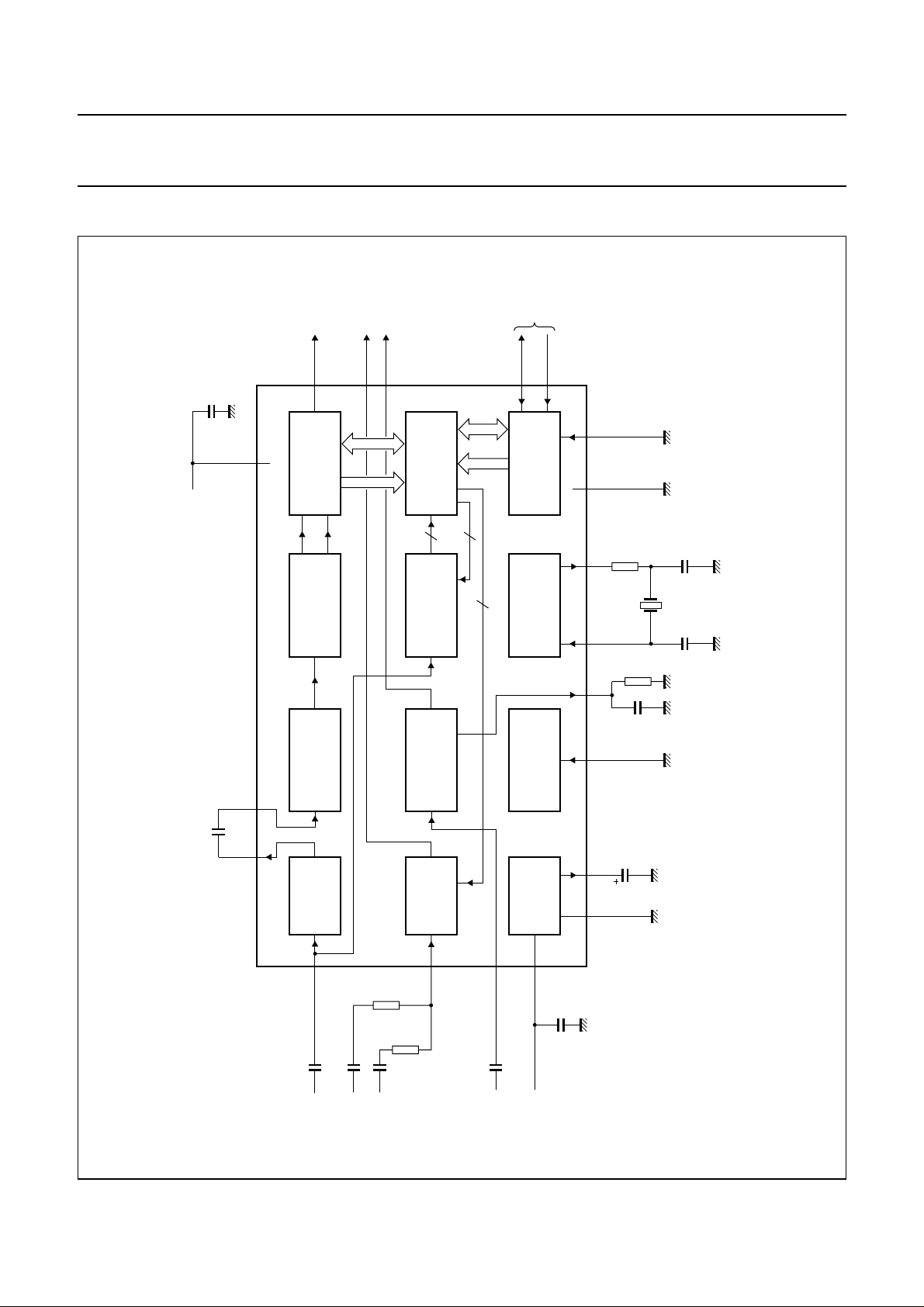
BLOCK DIAGRAM
C-BUS
2
data
available
pause
output
multi-path
output
I
handbook, full pagewidth
+5 V
C9
100 nF
DDD
71918
DAVN
8
DECODER
RDS/RDBS
RDS/RDBS
DEMODULATOR
CLOCKED
COMPARATOR
PSWN
MPTH
2
11
INTERFACE
4
SIGNAL QUALITY
SAA6588
MULTI-PATH
REGISTER
5
4
DETECTOR
DETECTOR
SDA
SCL
9
10
C-BUS SLAVE
2
TRANSCEIVER
I
AND CLOCK
OSCILLATOR
TEST
CONTROL
12
6
4
5
1
3
MAD
SSD
V
OSCO
OSCI
TCON MRO
R1
R4
C6
1 kΩ
Q1
470
100
kΩ
nF
MGK535
C5
MHz
n × 4.332
C4
82 pF
n = 1 to 4
47 pF
Fig.1 Block diagram.
C10
560 pF
SCOUT CIN V
57 kHz
8th ORDER
BAND-PASS
16
MPX
330 pF
C1
input
multiplex
0.47 µF
C2
0.47 µF
C3
audio
inputs
PAUSE
DETECTOR
13
AFIN
10
kΩ
R2
10
kΩ
R3
1997 Sep 01 4
C11
20
LVIN
level
2.2 nF
input
POWER
SUPPLY
AND RESET
14
DDA
V
+5 V
C8
1715
100 nF
ref
V
SSA
V
C7
2.2 µF

Philips Semiconductors Product specification
RDS/RBDS pre-processor SAA6588
PINNING
SYMBOL PIN DESCRIPTION
MRO 1 multi-path rectifier output
MPTH 2 multi-path detector output
TCON 3 test control input pin
OSCO 4 oscillator output
OSCI 5 oscillator input
V
V
SSD
DDD
6 digital ground (0 V)
7 digital supply voltage (5 V)
DAVN 8 data available output (active LOW)
MRO
OSCI
SSD
DDD
SDA
SCL
2
C-bus serial data I/O
2
C-bus serial clock input
LVIN
MGK533
20
19
18
17
16
15
14
13
12
11
CIN
SCOUT
V
MPX
V
V
AFIN
MAD
PSWN
1
2
3
4
5
6
7
8
9
10
SAA6588
ref
SSA
DDA
SDA 9 I
SCL 10 I
handbook, halfpage
MPTH
TCON
OSCO
V
V
DAVN
SYMBOL PIN DESCRIPTION
PSWN 11 pause switch output (active LOW)
MAD 12 slave address (LSB) input
AFIN 13 audio signal input
V
V
DDA
SSA
14 analog supply voltage (5 V)
15 analog ground (0 V)
MPX 16 multiplex input signal
V
ref
17 reference voltage output
SCOUT 18 band-pass filter output
CIN 19 comparator input
LVIN 20 level input
handbook, halfpage
MRO
MPTH
TCON
OSCO
OSCI
V
SSD
V
DDD
DAVN
SDA
SCL
1
2
3
4
5
SAA6588T
6
7
8
9
10
MGK534
20
19
18
17
16
15
14
13
12
11
LVIN
CIN
SCOUT
V
ref
MPX
V
SSA
V
DDA
AFIN
MAD
PSWN
Fig.2 Pin configuration (DIP20).
1997 Sep 01 5
Fig.3 Pin configuration (SO20).

Philips Semiconductors Product specification
RDS/RBDS pre-processor SAA6588
FUNCTIONAL DESCRIPTION
General
The following functions are performed by the SAA6588:
• Selection of the RDS/RBDS signal from the MPX input
signal
• 57 kHz carrier regeneration
• Demodulation of the RDS/RBDS signal
• Symbol decoding
• RDS/RBDS block detection
• Error detection and correction of transmission errors
• Fast block synchronization and synchronization control
• Detection of multi-path distortion and audio signal
pauses
• Determination of the signal quality
• Mode control of processing and RDS/RBDS data output
2
via I
C-bus interface
• Sensing of pause and multi-path, information via extra
output pins.
The block diagram of the RDS/RBDS pre-processor is
shown in Fig.1. For the application of the device only a few
external components are required. The pre-processors
functional blocks are described in the following sections.
RDS/RBDS signal demodulation
BAND-PASS FILTER
The band-pass filter has a centre frequency of 57 kHz.
It selects the RDS/RBDS sub-band from the multiplex
signal MPX and suppresses the audio signal components.
The filter block contains an analog anti-aliasing filter at the
input followed by an 8th order switched capacitor
band-pass filter and a reconstruction filter at the output.
C
LOCKED COMPARATOR
The comparator digitizes the output signal from the 57 kHz
band-pass filter for further processing by the digital
RDS/RBDS demodulator. To attain high sensitivity and to
avoid phase distortion, the comparator input stage
contains an automatic offset compensation.
D
EMODULATION
The demodulator provides all functions of the SAA6579
but has improved performance under weak signal
conditions.
The demodulator includes:
• 57 kHz carrier regeneration from the two sidebands
(Costas loop)
• Symbol integration over one RDS clock period
• Bi-phase symbol decoding
• Differential decoding
• Synchronization of RDS/RBDS output data with clock.
The RDS/RBDS demodulator recovers and regenerates
the continuously transmitted RDS/RBDS data stream out
of the multiplex signal (MPX) and provides the internal
signals clock (RDCL) and data (RDDA) for further
processing by the RDS/RBDS decoder block.
RDS/RBDS data processing
The RDS/RBDS data processing of the pre-processor
handles the complete processing and decoding of the
continuous serial RDS/RBDS demodulator output data
stream.
Different data processing modes are software controllable
2
by the external main controller via I
C-bus.
Processed RDS/RBDS data blocks, decoder status
information and signal quality information are also
available via I2C-bus.
RDS/RBDS
DECODER
The RDS/RBDS decoder contains:
• RDS/RBDS block detection
• Error detection and correction
• Synchronization
• Flywheel for synchronization hold
• Bit slip correction
• Data processing control
• RDS/RBDS data output.
1997 Sep 01 6

Philips Semiconductors Product specification
RDS/RBDS pre-processor SAA6588
RDS/RBDS block detection
The RDS/RBDS block detection is always active.
For a received sequence of 26 data bits, a valid block and
its offset are identified via syndrome calculation.
During synchronization search, the syndrome is calculated
with every new received data bit (bit-by-bit) for a received
26-bit sequence. If the decoder is synchronized, syndrome
calculation is activated only after 26 data bits for each new
block received.
Under RBDS reception situation, beside the RDS block
sequences with (A, B, C/C', D) offset also block sequences
of 4 blocks with offset E may be received. If the decoder
detects an E-block, this block is marked in the block
identification number BL and is available via I
request. In RBDS processing mode the block is signed as
valid E-block and in RDS processing mode, where only
RDS blocks are expected, signed as invalid E-block
(see Table 13).
This information can be used by the main controller to
detect E-block sequences and identify RDS or RBDS
transmitter stations.
2
C-bus
Error detection and correction
The RDS/RBDS error detection and correction recognizes
and corrects potential transmission errors within a
received block via parity-check in consideration of the
offset word of the expected block. Burst errors with a
maximum length of 5 bits are corrected with this method.
After synchronization has been found the error correction
is always active, but cannot be carried out in every
reception situation.
During synchronization search, the error correction is
disabled for detection of the first block and is enabled for
processing of the second block depending on the
pre-selected error correction mode for synchronization
(mode SYNCA to SYNCC, see Table 4).
The processed block data and the status of error
correction are available for data request via I2C-bus for the
last two blocks.
Processed blocks are characterized as uncorrectable
under the following conditions:
• During synchronization search, if the burst error is
higher than allowed by the pre-selected correction
mode.
• After synchronization has been found, if the burst error
is higher than 5 bits or if errors are detected but error
correction is not possible.
Synchronization
The decoder is synchronized if two successive valid blocks
in a valid sequence are detected by the block detection.
For detection of the second block of this sequence, error
correction is also enabled depending on the pre-selected
correction mode (see Table 4). Only valid (correctable)
blocks are accepted for synchronization (see also Section
“Error detection and correction”).
If synchronization is found, the synchronization status flag
(SYNC) is set and available via I2C-bus request.
The synchronization is held until the flywheel
(for synchronization hold) detects a loss of synchronization
(see Section “Flywheel for synchronization hold”) or an
external restart of synchronization is performed (see
Section “Data processing control”).
Flywheel for synchronization hold
For a fast detection of loss of synchronization the internal
flywheel counter checks the number of uncorrectable
blocks (error blocks). Error blocks increment and valid
blocks decrement the block error counter.
The flywheel counter is only active if the decoder is
synchronized. The synchronization is held until the
flywheel counter detects an error block overflow (loss of
synchronization). The maximum value for the error block
counter is adjustable via I2C-bus in a range of 0 to 63
(see Table 6).
The value 32 is set after reset and the values 0 and 63
have a special function.
• If the value 0 is programmed then no flywheel is active
• If the value 63 is programmed then the flywheel is
endless and no new start of synchronization is effected
automatically (synchronization hold).
Bit slip correction
During poor reception situation phase shifts of one bit to
the left or right (±1 bit slip) between the RDS/RBDS clock
and data may occur, depending on the lock conditions of
the demodulators clock regeneration.
If the decoder is synchronized and detects a bit slip, the
synchronization is corrected by +1 or −1 bit via block
detection on the respectively shifted expected new block.
1997 Sep 01 7

Philips Semiconductors Product specification
RDS/RBDS pre-processor SAA6588
Data processing control
The pre-processor provides different operating modes
selectable via the external I2C-bus. The data processing
control performs the pre-selected operating modes and
controls the requested output of the RDS/RBDS
information.
Restart of synchronization mode:
The ‘restart synchronization’ (NWSY) control mode
immediately terminates the actual synchronization and
restarts a new synchronization search procedure.
The NWSY flag is automatically reset after the restart of
synchronization by the decoder.
This mode is required for a fast new synchronization on
the RDS/RBDS data from a new transmitter station if the
tuning frequency is changed by the radio set.
Restart of synchronization search is furthermore
automatically carried out if the internal flywheel signals
a loss of synchronization (see Section “Flywheel for
synchronization hold”).
Error correction control mode for synchronization:
For error correction and identification of valid blocks
during synchronization search, three different modes
are selectable. (SYM1, SYM0, see Table 4).
RBDS processing mode:
The pre-processor is suitable for receivers intended for
the European (RDS) as well as for the USA (RBDS)
standard. If RBDS mode is selected via the I
block detection and the error detection and correction
are adjusted to RBDS data processing.
Data available control mode:
The pre-processor provides three different RDS/RBDS
data output processing modes selectable via the ‘data
available’ control mode: (see also Section “RDS/RBDS
data output” and Table 5).
Standard processing mode: if the decoder is
synchronized and a new block is received (every
26 bits), the actual RDS/RBDS information of the last
two blocks is available with every new received block.
Fast PI search mode: during synchronization search
and if a new A-block is received, the actual RDS/RBDS
information of this or the last two A-blocks respectively
is available with every new received A-block. If the
decoder is synchronized, the standard processing mode
is valid.
Reduced data request processing mode: if the
decoder is synchronized and two new blocks are
2
C-bus, the
received (every 52 bits), the actual RDS/RBDS
information of the last two blocks is available with every
two new received blocks.
The RDS/RBDS pre-processor provides data output of the
block identification, the RDS/RBDS information words and
error detection and correction status of the last two blocks
as well as signal quality indication and general decoder
status information.
In addition, the decoder controls also the data request from
the external main controller. The pre-processor activates
the ‘data overflow’ status flag DOFL
(see Section “Programming”), if the decoder is
synchronized and a new RDS/RBDS block is received
before the previously processed block was completely
transmitted via I
the interface registers are not updated until reset of the
data overflow flag by reading via the I2C-bus.
2
C-bus. After detection of data overflow
RDS/RBDS data output
The decoded RDS/RBDS block information and the
current pre-processor status is available via the I2C-bus.
For synchronization of data request between main
controller and pre-processor the additional data available
output signal is used.
If the decoder has processed new information for the main
controller the data available signal (DAVN) is activated
(LOW) under the following conditions (see also Table 5):
• During synchronization search in DAVB mode if a valid
A-block has been detected. This mode can be used for
fast search tuning (detection and comparison of the PI
code contained in the A-block).
• During synchronization search in any DAV mode, if two
blocks in correct sequence have been detected
(synchronization criterion).
• If the pre-processor is synchronized and in mode DAVA
and DAVB a new block has been processed. This mode
is the standard data processing mode, if the decoder is
synchronized.
• If the pre-processor is synchronized and in DAVC mode
two new blocks have been processed.
• If the pre-processor is synchronized and in any DAV
mode loss of synchronization is detected (flywheel
counter overflow and resulting restart of
synchronization).
• In any DAV mode, if a reset condition caused by
power-on or voltage-drop is detected.
1997 Sep 01 8

Philips Semiconductors Product specification
RDS/RBDS pre-processor SAA6588
The processed RDS/RBDS data are available for I2C-bus
request for at least 20 ms after the DAVN signal was
activated.
The DAVN signal is always automatically deactivated
(HIGH) after 10 ms or almost after the main controller has
read the RDS/RBDS data via I2C-bus (see Fig.4).
The decoder ignores new processed RDS/RBDS blocks if
the DAVN signal is active or if data overflow occurs
(see Section “Data processing control”).
Multi-path detector
The multi-path detector takes its information from the
unweighted level signal of the FM IF amplifier, input LVIN
(see Fig.1). The part of frequency components around
21 kHz is selected by a band-pass filter and rectified by a
full-wave rectifier. The capacitor at pin MRO is the charge
capacitor. In combination with internal current sources the
time constants of the rectifier are defined.
The analogous output voltage of the multi-path rectifier is
buffered and available via pin MPTH.
Signal quality detector
The signal quality detector takes its information from the
multiplex signal. Disturbances caused by
adjacent-channel reception, noise, or multi-path, generate
high frequency components (noise) on the multiplex signal
besides the audible distortion.
The signal quality measurement is provided for fast testing
alternative frequencies as well as for the tuned frequency.
It is a short start/stop procedure. The measuring time is
limited to 850 µs. To attain an average value over a longer
time, multiple measurements are possible with integration
by software processing.
The noise is detected from the frequency spectrum above
90 kHz. The noise voltage is selected by a 4th order
high-pass filter. A full-wave rectifier, controlled by this
noise voltage, charges an initially discharged capacitor (on
chip). The time is measured until the voltage across the
capacitor has reached a defined threshold value. Then
that time equivalent value is stored. The resolution of the
signal quality measurement is 4 bits (16 steps).
For operating the noise detector two modes are provided,
the triggered mode and the continuous mode. The mode is
defined by the bit SQCM (Signal Quality Continuous
Measurement) as described in Section “Programming”.
The triggered mode is provided for a fast signal quality test
of e.g. an alternative frequency. After the alternative
frequency has been tuned, the signal quality detector has
to be started (triggered) by transmitting the bits SQCM = 0
and TSQD = 1 via the I2C-bus (see Fig.5). This causes a
single shot measurement immediately after the
acknowledgement of this byte. The bit TSQD is internally
reset during the measurement (TSQD = 0). The result of
the measurement is stored and is available for reading out,
as long as no new measurement is started again e.g. after
tuning back to the previous frequency.
The continuous mode minimizes the required I2C-bus
activities for multiple measurements. After transmission of
SQCM = 1 and TSQD = 1, the signal quality detector
starts a new measurement as described above. But every
time after finishing one measuring procedure the result is
stored (overwrites the previous value within the I2C-bus
buffer SQI3 to SQI0) and a new measurement starts
automatically. If at any time the pre-processor is read out
by his master, the last measured value will be transmitted.
After transmitting the control information SQCM = 0 and
TSQD = 0, the measurement activity will be stopped.
A previously started but not yet finished measurement will
be completed and this last result will also be available.
The control bit combination SQCM = 1 and TSQD = 0
must not be used. It is reserved for later applications.
At a maximum time of 850 µs after triggering or automatic
restart of the signal quality detector, the result of the
measurement (signal quality indication) is available and
represented by the four bits SQI3 to SQI0, in a value range
of 0 to 15 and is available via the I2C-bus
(see Section “Programming”). The result 0 characterizes
no or less noise/distortion and 15 high noise/distortion.
Tolerances of the signal quality detector as well as
characteristics and tolerances of the FM IF amplifier can
be compensated by adjusting the sensitivity of the signal
quality detector with the control bits SQS0 to SQS4.
The sensitivity can be adjusted over a range of 18.6 dB
(−9.0 to +9.6 dB) in steps of 0.6 dB as given in Table 10.
Pause detector
The pause detector watches the audio modulation for
pauses or very low levels. This function can be used for
performing inaudible RDS AF-tests if the radio is in FM
mode as well as for Automatic Music Search (AMS) if the
radio is in cassette mode.
The input of the pause detector (AFIN) is low-ohmic and
must be current driven (negative input of an operational
amplifier). This has the following advantages:
1997 Sep 01 9
 Loading...