

Philips SAA6581T Datasheet

INTEGRATED CIRCUITS
DATA SH EET
SAA6581T
RDS/RBDS demodulator
Product specification
File under Integrated Circuits, IC01
2001 May 07

Philips Semiconductors Product specification
RDS/RBDS demodulator SAA6581T
FEATURES
• Integrated switched capacitor filter
• Demodulates European Radio Data System (RDS) or
the USA Radio Broadcast Data System (RBDS) signals
• Oscillator frequencies: 4.332 or 8.664 MHz
• Integrated ARI clamping
• CMOS device
• Single supply voltage: 5 V
• Extended temperature range: −40 to +85 °C
• Low number of external components.
GENERAL DESCRIPTION
The RDS/RBDS demodulator is a CMOS device with
integrated filtering and demodulating of RDS/RBDS
signals comingfrom a multiplexed input data stream. Data
signal RDDA and clock signal RDCL are provided as
outputs for further processing by a suitable
microcomputer, for example CCR921 and CCR922.
The SAA6581T replaces SAA6579 in function and
pin-compatibility.
APPLICATIONS
The RDS/RBDS system offers a large range of
applications from the many functions that can be
implemented. For car radios the most important are:
• Program Service (PS) name
• Traffic Program (TP) identification
• Traffic Announcement (TA) signal
• Alternative Frequency (AF) list
• Program Identification (PI)
• Enhanced Other Networks (EON) information.
QUICK REFERENCE DATA
SYMBOL PARAMETER MIN. TYP. MAX. UNIT
V
DDA
V
DDD
I
DD(tot)
V
i(MPX)
f
i(xtal)
analog supply voltage 4.0 5.0 5.5 V
digital supply voltage 4.0 5.0 5.5 V
total supply current − 6.0 − mA
RDS input sensitivity at pin MPX 1 −−mV
crystal input frequency − 4.332 − MHz
− 8.664 − MHz
ORDERING INFORMATION
TYPE
NUMBER
NAME DESCRIPTION VERSION
PACKAGE
SAA6581T SO16 plastic small outline package; 16 leads; body width 7.5 mm SOT162-1
2001 May 07 2

Philips Semiconductors Product specification
RDS/RBDS demodulator SAA6581T
BLOCK DIAGRAM
handbook, full pagewidth
multiplex
input
+5 V
100 nF
330 pF
C2
C1
MPX
V
DDA
4
5
8th ORDER
BANDPASS FILTER
POWER
SUPPLY
AND RESET
6
V
SSAVref
57 kHz
560 pF
C6
87
SAA6581T
TEST
CONTROL
15
TCON
C3
2.2 µF
Fig.1 Block diagram.
CINSCOUT
CLOCKED
COMPARATOR
9
MODE
47 pF
OSCILLATOR
AND CLOCK
13 14
OSCIQ1OSCO
C4
+5 V
V
DDD
12
RDS/RBDS
DEMODULATOR
SIGNAL QUALITY
DETECTOR
C5
56 pF
113
V
SSD
C7
100 nF
10
SYNC
RDCL
16
2
RDDA
1
QUAL
MHB899
2001 May 07 3
Philips Semiconductors Product specification
RDS/RBDS demodulator SAA6581T
PINNING
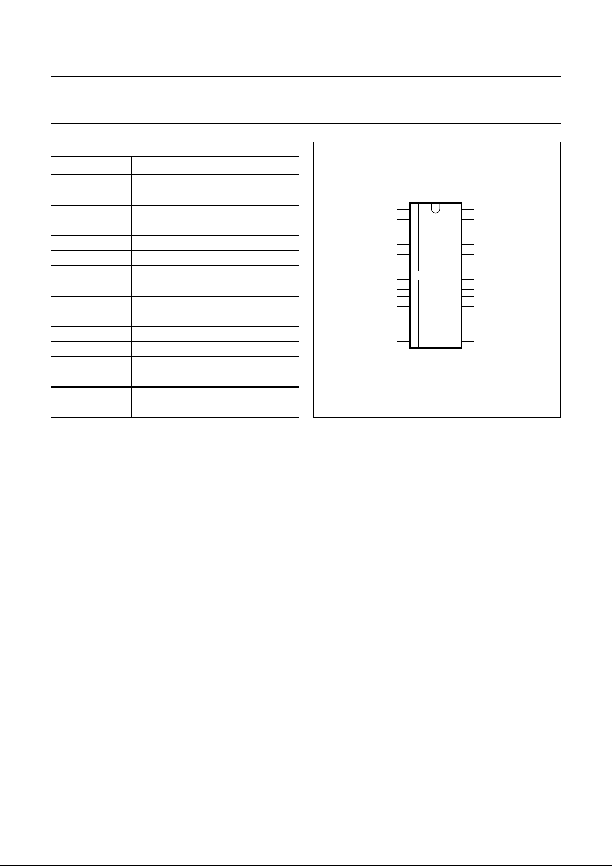
SYMBOL PIN DESCRIPTION
QUAL 1 signal quality indication output
RDDA 2 RDS data output
V
ref
3 reference voltage output (1/2V
MPX 4 multiplex signal input
V
V
DDA
SSA
5 analog supply voltage (5 V)
6 analog ground (0 V)
CIN 7 comparator input
SCOUT 8 switched capacitor filter output
MODE 9 oscillator frequency select input
SYNC 10 ARI clamping control input
V
V
SSD
DDD
11 digital ground (0 V)
12 digital supply voltage (5 V)
OSCI 13 oscillator input
OSCO 14 oscillator output
TCON 15 test control input
RDCL 16 RDS clock output
DDA
)
handbook, halfpage
1
QUAL
2
RDDA
3
V
ref
4
MPX
V
DDA
V
SSA
CIN
SCOUT
SAA6581T
5
6
7
8
MHB900
Fig.2 Pin configuration.
16
15
14
13
12
11
10
9
RDCL
TCON
OSCO
OSCI
V
DDD
V
SSD
SYNC
MODE
FUNCTIONAL DESCRIPTION
RDS/RBDS signal demodulation
BANDPASS FILTER
The bandpass filter has a centre frequency of 57 kHz. It
selects the RDS/RBDSsub-band fromthe multiplex signal
MPX and suppresses the audio signal components. The
filter block contains an analog anti-aliasing filter at the
inputfollowedby an 8thorderswitched capacitor bandpass
filter and a reconstruction filter at the output.
CLOCKED COMPARATOR
Thecomparator digitizestheoutput signalfromthe 57 kHz
bandpass filter for further processing by the digital
RDS/RBDS demodulator. To attain high sensitivity and to
avoid phase distortion, the comparator input stage has
automatic offset compensation.
DEMODULATOR
The demodulator provides all functions of the SAA6579
and improves performance under weak signal conditions.
Demodulator functions include:
• 57 kHz carrier regeneration from the two sidebands
(Costas loop)
• Symbol integration over one RDS clock period
• Bi-phase symbol decoding
• Differential decoding
• Synchronization of RDS/RBDS output data.
The RDS/RBDS demodulator recovers and regenerates
the continuously transmitted RDS/RBDS data stream in
the MPX signal and provides clock RDCL for the output
signalsand dataoutput RDDA forfurther processingby an
RDS/RBDS decoder, for example CCR921 or CCR922.
ARI CLAMP
The demodulator checks the input signal for presence of
RDS only, or RDS plus ARI transmissions. After a fixed
test period, if the SYNC inputis setHIGH the demodulator
locksin the ‘verified’condition(seeTable 1). If SYNCisset
LOW, the ARI clamping is reset (disabled). After SYNC
returns to HIGH, the demodulator resumes checking the
input signal.
2001 May 07 4

Philips Semiconductors Product specification
RDS/RBDS demodulator SAA6581T
Table 1 Control pin SYNC
SYNC ARI CLAMPING
LOW internal ARI clamping disabled
HIGH ARI clamping allowed to be logged
SIGNAL QUALITY DETECTION
Output QUAL indicates thesafety ofthe regeneratedRDS
Table 2 Control pins TCON and MODE
TCON MODE OSCILLATOR FREQUENCY
HIGH LOW 4.332 MHz
HIGH HIGH 8.664 MHz
The clock generator generates the internal 4.332 MHz
system clock and timing signal derivatives.
data (HIGH = ‘good’ data; LOW = ‘unsafe’ data).
Power supply and internal reset
Oscillator and system clock generator
For good performance of the bandpass and demodulator
stages, the demodulator requires a crystal oscillator with a
frequency of 4.332 or 8.664 MHz. The demodulator can
operatewith eitherfrequency(see Table 2),so that aradio
set with a microcontroller can run, in this case, with one
crystal only. The demodulator oscillator can drive the
Thedemodulator hasseparate power supplyinputs forthe
digital and analog parts of the device. For the analog
functions an additional reference voltage (1⁄2V
DDA
) is
internally generated and available via the output pin V
The demodulator requires a defined reset condition. The
demodulator generates automatically a reset signal after
the power supplyV
is switched on,or ata voltage-drop.
DDA
microcontroller, or vice versa.
LIMITING VALUES
In accordance with the Absolute Maximum Rating System (IEC 60134).
SYMBOL PARAMETER CONDITIONS MIN. MAX. UNIT
V
DD
V
n
I
i
I
lu(prot)
supply voltage 0 6.5 V
voltage at pins 1 to 4, 7 to 10, and
13 to 16 with respect to pins 6 and 11
inputcurrent atpins 1 to 5, 7 to 11 and
13 to 16
latch-up protection current in pulsed
mode
pins 5 and 12 are
connected to V
DD
pins 6 and 11 are
connected to ground
T
= −40 to +85 °C with
amb
voltage limiting −2 to +10 V
T
=25°C with voltage
amb
−0.5 VDD+ 0.5 ≤ 6.5 V
−10 +10 mA
−100 +100 mA
−200 +200 mA
limiting −2 to +12 V
= −40 to +85 °C
T
amb
−10 +10 mA
without voltage limiting
T
amb
T
stg
V
es
ambient temperature −40 +85 °C
storage temperature −65 +150 °C
electrostatic handling voltage note 1 −4000 +4000 V
note 2 −500 +500 V
ref
.
Notes
1. Human body model (equivalent to discharging a 100 pF capacitor through a 1.5 kΩ series resistor).
2. Machine model (equivalent to discharging a 200 pF capacitor through a0 Ω series resistorand 0.75 µH inductance).
THERMAL CHARACTERISTICS
SYMBOL PARAMETER CONDITIONS VALUE UNIT
R
th(j-a)
thermal resistance from junction to ambient in free air 104 K/W
2001 May 07 5
 Loading...