

Philips saa5700 DATASHEETS

INTEGRATED CIRCUITS
DATA SH EET
SAA5700
Chinese Character System Teletext
(CCST) decoder
Preliminary specification
File under Integrated Circuits, IC02
1997 May 16

Philips Semiconductors Preliminary specification
Chinese Character System Teletext
(CCST) decoder
FEATURES
• Acquisition and display of the 625-line PAL CCST
Chinese standard for teletext, with Chinese and Latin
character sets
• Supports multiple DRAM sizes: 256K × 4 bits,
1M × 4 bits, 4M × 4 bits and 2 × 1M × 4 bits with an
additional decoder/demultiplexer IC
• Acquires and stores in background up to (typically)
400 pages with 1M × 4 bits external DRAM
• CCST Fastext, with capability of displaying Chinese
characters on Fastext prompt row
• Meshing for reduced contrast video background in
subtitles and boxes
• Full line and screen colour to all edges of screen
• Supports 625-line 50/100 Hz display modes
• Scan-locked and stand-alone sync modes; supports
video-locked sync modes with external PLL
2
• Easy control via high level I
• Sync mode switching and picture centring via I2C-bus
SAFARI commands
• Supports external decryption unit for encrypted data.
C-bus SAFARI commands
SAA5700
GENERAL DESCRIPTION
The SAA5700 is a Chinese teletext decoder suitable for TV
and multimedia applications. It incorporates all the data
slicing, acquisition and display circuitry on-chip, as well as
the logic for memory management. An external DRAM is
used to store the currently displayed page and also the
precaptured teletext pages.
An external ROM is used to store the ideographic Chinese
character set. There is a high level software interface with
easy commands for the control of the decoder. Control is
achieved via the I2C-bus.
The device is available in a QFP64 package.
ORDERING INFORMATION
PACKAGE
TYPE NUMBER
NAME DESCRIPTION VERSION
SAA5700GP QFP64 plastic quad flat package; 64 leads (lead length 1.95 mm);
body 14 × 20 × 2.8 mm
SOT319-2
1997 May 16 2

Philips Semiconductors Preliminary specification
Chinese Character System Teletext
(CCST) decoder
BLOCK DIAGRAM
handbook, full pagewidth
BLACK
CVBS
REF+
STN
I
REF
V
DDD1VSS1VDDD2VSS2VSS3VDDXVSSOVDDAVSSAVSS
33 48 49 2 19 20 9 8 14,16,
35
4
5
10
6
7
SYNC
SEPARATOR
DATA
ACQUISITION
FRONT END
12 MHz
ACQUISITION
TIMING
OSCILLATOR
AND CLOCK
GENERATOR
6 MHz
SAA5700
26
1
OSCOUT
64
OSCIN
59
RESET
ROMCS
RAS
CAS
RA10 to RA0
RD7 to RD0
WE
27
42
53
44
54, 41, 40,
38 to 36,
32 to 28
55 to 58,
52, 51,
47, 46
PACKET
BUFFER
MEMORY
INTERFACE
SAA5700
BUS
PROCESSOR
BLOCK
24 MHz
DISPLAY
INTERFACE
DISPLAY
TIMING
DISPLAY SECTION
63
60
61
62
21
22
23
24
17
18
25
MGG539
DCL
DDA
SCL
SDA
R
G
B
BLAN
LFB
FFB/STTV
ODD/EVEN
Fig.1 Block diagram.
1997 May 16 3
Philips Semiconductors Preliminary specification
Chinese Character System Teletext
SAA5700
(CCST) decoder
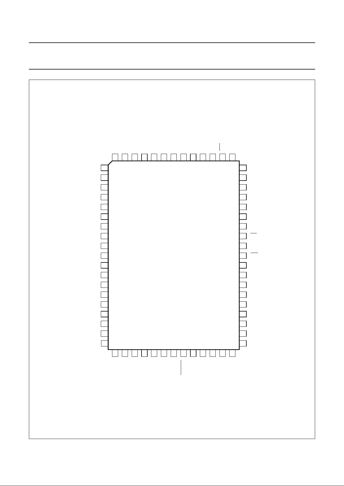
PINNING
SYMBOL PIN I/O DESCRIPTION
OSCOUT 1 O oscillator output to crystal
V
SS3
n.c. 3 − not connected
BLACK 4 I/O black level sample and hold capacitor; 100 nF to V
CVBS 5 I video signal input; 100 nF series capacitor, 250Ω source impedance maximum,
STN 6 I/O ADC current reference decoupling; 100 nF to V
I
REF
V
SSA
V
DDA
REF+ 10 I ADC voltage reference decoupling; 100 nF to V
i.c. 11 − internally connected; do not use
i.c. 12 − internally connected; do not use
i.c. 13 − internally connected; do not use
V
SS
n.c. 15 − not connected
V
SS
LFB 17 I scan line flyback input (HSYNC)
FFB/STTV 18 I/O scan field flyback input (VSYNC)/sync to TV output
V
DDX
V
SSO
R 21 O analog Red output
G 22 O analog Green output
B 23 O analog Blue output
BLAN 24 O fast blanking (VDS)
ODD/EVEN 25 O frame rate signal for hardware de-interlace (FRAME)
V
SS
ROMCS 27 O chip select (address decode) for ROM
RA0 28 O bit 0 of address to DRAM, ROM and IC
RA1 29 O bit 1 of address to DRAM, ROM and IC
RA2 30 O bit 2 of address to DRAM, ROM and IC
RA3 31 O bit 3 of address to DRAM, ROM and IC
2 ground ground for I/O pad buffers connect to VSS; internally connected to V
SSA
reference to V
7 I current reference input; 10 kΩ to V
SSA
SSA
SSA
8 ground 0 V power supply; analog
9 supply +5 V power supply; analog
SSA
14 ground connect to VSS for normal use
16 ground connect to VSS for normal use
19 supply +5 V power supply; connect to VDD for normal use
20 ground output stage current return and 0 V
26 ground connect to VSS for normal use
SS1
and V
SS2
1997 May 16 4

Philips Semiconductors Preliminary specification
Chinese Character System Teletext
(CCST) decoder
SYMBOL PIN I/O DESCRIPTION
RA4 32 O bit 4 of address to DRAM, ROM and IC
V
SS1
n.c. 34 − not connected
V
DDD1
RA5 36 O bit 5 of address to DRAM, ROM and IC
RA6 37 O bit 6 of address to DRAM, ROM and IC
RA7 38 O bit 7 of address to DRAM, ROM and IC
n.c. 39 − not connected
RA8 40 O bit 8 of address to DRAM, ROM and IC
RA9 41 O bit 9 of address to DRAM, ROM and IC
RAS 42 O row address strobe to DRAM; active LOW
n.c. 43 − not connected
WE 44 O write enable to DRAM and IC; active LOW
i.c. 45 − internally connected; do not use
RD0 46 I/O bit 0 of data bus to/from DRAM, ROM and IC
RD1 47 I/O bit 1 of data bus to/from DRAM, ROM and IC
V
DDD2
V
SS2
n.c. 50 − not connected
RD2 51 I/O bit 2 of data bus to/from DRAM, ROM and IC
RD3 52 I/O bit 3 of data bus to/from DRAM, ROM and IC
CAS 53 O column address strobe to DRAM; active LOW
RA10 54 O bit 10 of address to DRAM, ROM and IC
RD7 55 I/O bit 7 of data bus to/from DRAM, ROM and IC
RD6 56 I/O bit 6 of data bus to/from DRAM, ROM and IC
RD5 57 I/O bit 5 of data bus to/from DRAM, ROM and IC
RD4 58 I/O bit 4 of data bus to/from DRAM, ROM and IC
RESET 59 I chip/processor reset input (active HIGH)
DDA 60 I/O bidirectional serial data to/from optional Decryptor
SCL 61 I primary I
SDA 62 I/O primary I
DCL 63 O serial clock to optional Decryptor
OSCIN 64 I oscillator input from crystal/external clock input
33 ground 0 V power supply digital; connected internally to V
35 supply +5 V power supply digital; connected internally to V
48 supply +5 V power supply digital; connected internally to V
49 ground 0 V power supply digital; connected internally to V
2
C-bus serial clock input
2
C-bus serial data
SS2
DD2
DD1
SS1
and V
and V
SAA5700
SS3
SS3
1997 May 16 5
Philips Semiconductors Preliminary specification
Chinese Character System Teletext
(CCST) decoder
handbook, full pagewidth
DCL
SDA
SCL
62
61
OSCOUT
V
SS3
n.c.
BLACK
CVBS
STN
I
REF
V
SSA
V
DDA
REF+
i.c.
i.c.
i.c.
V
SS
n.c.
V
SS
LFB
FFB/STTV
V
DDX
OSCIN
64
63
1
2
3
4
5
6
7
8
9
10
11
12
13
14
15
16
17
18
19
DDA
60
SAA5700
RESET
59
RD4
58
RD5
57
RD6
56
RD7
55
RA10
54
CAS
53
RD3
52
SAA5700
51
RD2
n.c.
50
V
49
SS2
V
48
DDD2
RD1
47
RD0
46
i.c.
45
WE
44
n.c.
43
RAS
42
RA9
41
RA8
40
n.c.
39
RA7
38
RA6
37
RA5
36
V
35
DDD1
n.c.
34
V
33
SS1
20
21
22
23
24
25
B
G
BLAN
ODD/EVEN
SSO
V
R
Fig.2 Pin configuration.
1997 May 16 6
26
V
SS
27
28
RA0
ROMCS
29
RA1
30
RA2
31
RA3
32
RA4
MGG538

Philips Semiconductors Preliminary specification
Chinese Character System Teletext
SAA5700
(CCST) decoder
HIGH LEVEL I2C-BUS COMMAND INTERFACE
This device communicates via the I2C-bus using the SAFARI protocol. The following section indicates the protocol which
is supported by this decoder.
User commands
Table 1 lists the CCST user command codes in TV mode; Table 2 lists the CCST user command codes in Text mode.
Table 1 TV mode user command codes
FUNCTION ID
(HEX)
00 −
01 −
02 −
03 PICTURE
04 STATUS
05 −
06 −
07 TIME
08 −
09 −
0A −
0B −
0C −
0D −
0E −
0F −
10 TV PROGRAMME 0
11 TV PROGRAMME 1
12 TV PROGRAMME 2
13 TV PROGRAMME 3
14 TV PROGRAMME 4
15 TV PROGRAMME 5
16 TV PROGRAMME 6
17 TV PROGRAMME 7
18 TV PROGRAMME 8
19 TV PROGRAMME 9
1A TV PROGRAMME10
1B TV PROGRAMME11
1C TV PROGRAMME 12
1D TV PROGRAMME 13
1E TV PROGRAMME14
1F TV PROGRAMME 15
FUNCTION
Table 2 Text mode user command codes
FUNCTION ID
(HEX)
20 RED
21 GREEN
22 YELLOW
23 SUBTITLE
24 STATUS
25 HOLD TOGGLE
26 REVEAL
27 CANCEL TOGGLE
28 INDEX
29 −
2A BROWSE
2B REVEAL SET TOGGLE
2C −
2D PREVIOUS
2E DISPLAY CHINESE PROMPT
2F SUBCODE TOGGLE
30 1
31 2
32 3
33 4
34 5
35 6
36 7
27 8
28 9
29 0
3A SIZE
3B UP
3C DOWN
3D CYAN
3E MIX
3F TEXT
FUNCTION
1997 May 16 7

Philips Semiconductors Preliminary specification
Chinese Character System Teletext
SAA5700
(CCST) decoder
Extended commands
The extended commands for the decoder are listed in Table 3.
Table 3 Extended commands
OBJECT FUNCTION
NAME
Display 48 set sync mode 04 1 − sync mode none
Processor 52 restart software 06 3 − FFFFFCH none
Memory and OSD 53 read packet 03 1
ID
(HEX)
NAME
set display
position
write packet 06 1
OSD mode on 08 0 − none none
OSD mode off 0A 0 − none none
OSD display 0E 0 − none none
clear display page 10 0 − none none
(HEX)
08 4 −
PARAMETER LENGTH
(BYTES)
ID
INPUT OUTPUT INPUT OUTPUT
[+1]
+40
PARAMETERS
row start, line start none
40 packet number,
[Designation
code]
− packet number,
packet data
packet data
none
1997 May 16 8
 Loading...