

Philips SAA5551PS-M2A, SAA5552PS-M2A, SAA5553PS-M2A Datasheet

DATA SH EET
Preliminary specification
File under Integrated Circuits, IC02
1999 Oct 27
INTEGRATED CIRCUITS
SAA55xx
Standard TV microcontrollers with
On-Screen Display (OSD)

1999 Oct 27 2
Philips Semiconductors Preliminary specification
Standard TV microcontrollers with
On-Screen Display (OSD)
SAA55xx
CONTENTS
1 FEATURES
2 GENERAL DESCRIPTION
3 QUICK REFERENCE DATA
4 ORDERING INFORMATION
5 BLOCK DIAGRAM
6 PINNING INFORMATION
6.1 Pinning
6.2 Pin description
7 MICROCONTROLLER
7.1 Microcontroller features
8 MEMORY ORGANISATION
8.1 Security bits - program and verify
8.2 RAM organisation
8.3 Data memory
8.4 SFR memory
8.5 Character set feature bits
8.6 External (auxiliary) memory
9 POWER-ON RESET
10 REDUCED POWER MODES
10.1 Idle mode
10.2 Power-down mode
10.3 Standby mode
11 I/O FACILITY
11.1 I/O ports
11.2 Port type
11.3 Port alternate functions
11.4 LED support
12 INTERRUPT SYSTEM
12.1 Interrupt enable structure
12.2 Interrupt enable priority
12.3 Interrupt vector address
12.4 Level/edge interrupt
13 TIMER/COUNTER
14 WATCHDOG TIMER
14.1 Watchdog Timer operation
15 PULSE WIDTH MODULATORS
15.1 PWM control
15.2 Tuning Pulse Width Modulator (TPWM)
15.3 Software ADC (SAD)
16 I2C-BUS SERIAL I/O
16.1 I2C-bus port selection
17 MEMORY INTERFACE
17.1 Memory structure
17.2 Memory mapping
17.3 Addressing memory
17.4 Page clearing
18 DATA CAPTURE
18.1 Data Capture Features
18.2 Broadcast service data detection
18.3 VPS acquisition
18.4 WSS acquisition
19 DISPLAY
19.1 Display features
19.2 Display mode
19.3 Display feature descriptions
19.4 Character and attribute coding
19.5 Screen and global controls
19.6 Screen colour
19.7 Text display control
19.8 Display positioning
19.9 Character set
19.10 Display synchronization
19.11 Video/data switch (fast blanking) polarity
19.12 Video/data switch adjustment
19.13 RGB brightness control
19.14 Contrast reduction
20 MEMORY MAPPED REGISTERS
21 LIMITING VALUES
22 CHARACTERISTICS
22.1 I2C-bus characteristics
23 QUALITY AND RELIABILITY
23.1 Group A
23.2 Group B
23.3 Group C
24 APPLICATION INFORMATION
25 ELECTROMAGNETIC COMPATIBILITY
(EMC) GUIDELINES
26 PACKAGE OUTLINE
27 SOLDERING
27.1 Introduction to soldering through-hole mount
packages
27.2 Soldering by dipping or by solder wave
27.3 Manual soldering
27.4 Suitability of through-hole mount IC packages
for dipping and wave soldering methods
28 DEFINITIONS
29 LIFE SUPPORT APPLICATIONS
30 PURCHASE OF PHILIPS I2C COMPONENTS
1999 Oct 27 3
Philips Semiconductors Preliminary specification
Standard TV microcontrollers with
On-Screen Display (OSD)
SAA55xx
1 FEATURES
• Single-chip microcontroller with integrated On-Screen
Display (OSD)
• Versions available with integrated data capture
• One Time Programmable (OTP) memory for both
program Read Only Memory (ROM) and character sets
• Single power supply: 3.0 to 3.6 V
• 5 V tolerant digital inputs and I/O
• 29 I/O lines via individual addressable controls
• Programmable I/O for push-pull, open-drain and
quasi-bidirectional
• Two port lines with 8 mA sink (at <0.4 V) capability, for
direct drive of Light Emitting Diode (LED)
• Single crystal oscillator for microcontroller, OSD and
data capture
• Power reduction modes: Idle and Power-down
• Byte level I2C-bus with dual port I/O
• Pin compatibility throughout family
• Operating temperature: −20 to +70 °C.
2 GENERAL DESCRIPTION
The SAA55xx standard family of microcontrollers are a
derivative of the Philips industry-standard 80C51
microcontroller, and are intended for use as the central
control mechanism in a television receiver. They provide
controlfunctionsforthetelevisionsystem,OSD,andsome
versions include an integrated data capture and display
function.
The data capture hardware has the capability of decoding
and displaying both 525 and 625-line World System
Teletext (WST), Video Programming System (VPS) and
Wide Screen Signalling (WSS) information. The same
displayhardwareisusedbothforTeletext and OSD, which
means that the display features available give greater
flexibility to differentiate the TV set.
The SAA55xx standard family offers a range of
functionality from non-text, 16-kbyte program ROM and
256-byte Random Access Memory (RAM), to a 10-page
text version, 64-kbyte program ROM and 1.2-kbyte RAM.
3 QUICK REFERENCE DATA
SYMBOL PARAMETER MIN. TYP. MAX. UNIT
Supply
V
DDX
any supply voltage (VDDto VSS) 3.0 3.3 3.6 V
I
DDP
periphery supply current 1 −−mA
I
DDC
core supply current − 15 18 mA
I
DDC(id)
Idle mode core supply current − 4.6 6 mA
I
DDC(pd)
Power-down mode core supply current − 0.76 1 mA
I
DDC(stb)
Standby mode core supply current − 5.11 6.50 mA
I
DDA
analog supply current − 45 48 mA
I
DDA(id)
Idle mode analog supply current − 0.87 1.0 mA
I
DDA(pd)
Power-down mode analog supply current − 0.45 0.7 mA
I
DDA(stb)
Standby mode analog supply current − 0.95 1.20 mA
f
xtal
crystal frequency − 12 − MHz
T
amb
operating ambient temperature −20 − +70 °C
T
stg
storage temperature −55 − +125 °C
1999 Oct 27 4
Philips Semiconductors Preliminary specification
Standard TV microcontrollers with
On-Screen Display (OSD)
SAA55xx
4 ORDERING INFORMATION
Notes
1. ‘nnnn’ is a four digit number uniquely referencing the microcontroller program mask.
2. For details of the LQFP100 package, please contact your local regional office for availability.
TYPE NUMBER
(1)
PACKAGE
(2)
ROM RAM
TEXT
PAGES
NAME DESCRIPTION VERSION
SAA5500PS/nnnn SDIP52 plasticshrink dual in-line package;
52 leads (600 mil)
SOT247-1 16-kbyte 256-byte −
SAA5501PS/nnnn 32-kbyte 512-byte −
SAA5502PS/nnnn 48-kbyte 256-byte −
SAA5503PS/nnnn 64-kbyte 512-byte −
SAA5520PS/nnnn 16-kbyte 256-byte 1
SAA5521PS/nnnn 32-kbyte 512-byte 1
SAA5522PS/nnnn 48-kbyte 750-byte 1
SAA5523PS/nnnn 64-kbyte 1-kbyte 1
SAA5551PS/nnnn 32-kbyte 750-byte 10
SAA5552PS/nnnn 48-kbyte 1-kbyte 10
SAA5553PS/nnnn 64-kbyte 1.2-kbyte 10
1999 Oct 27 5
Philips Semiconductors Preliminary specification
Standard TV microcontrollers with
On-Screen Display (OSD)
SAA55xx
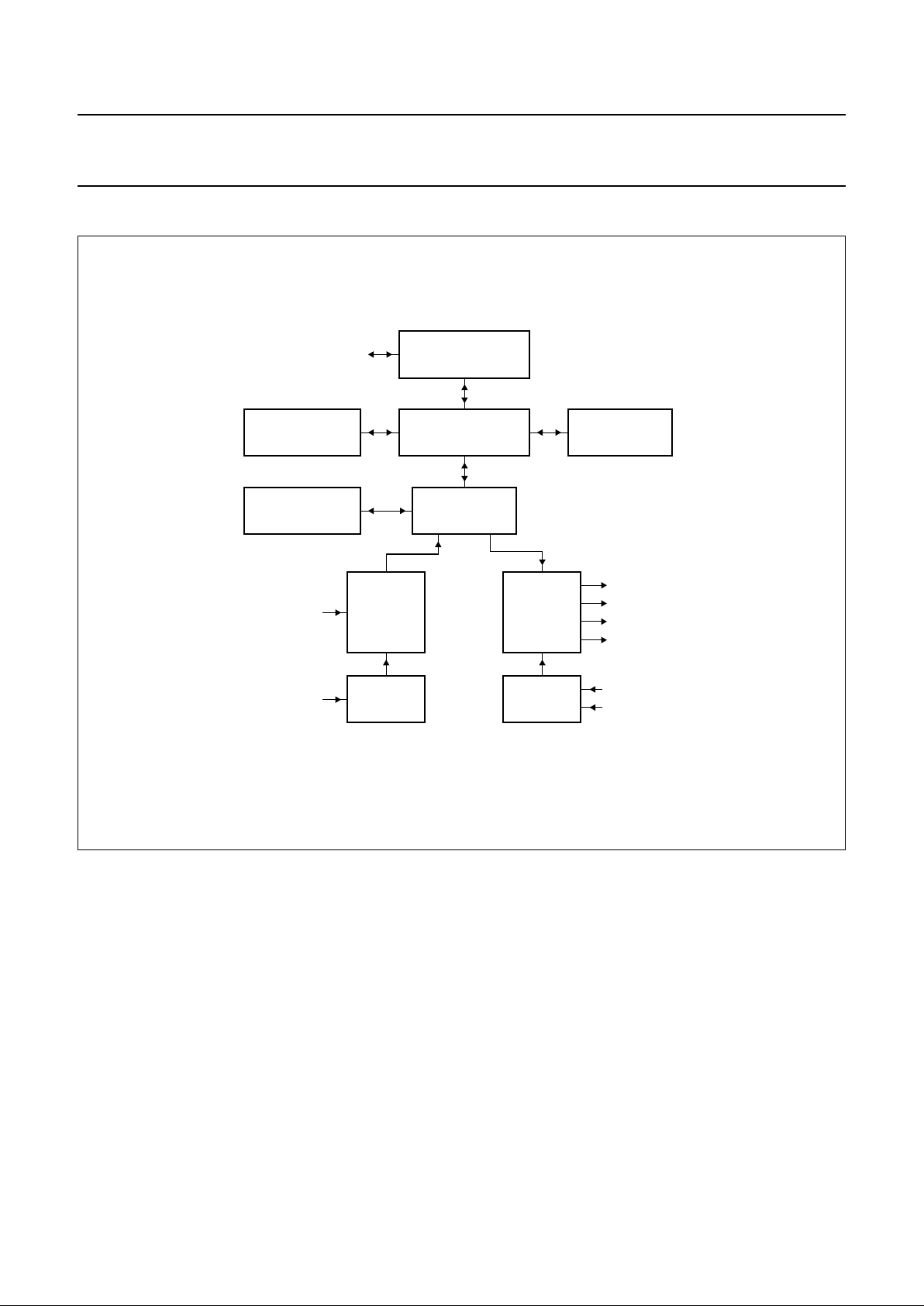
5 BLOCK DIAGRAM
Fig.1 Block diagram (top level architecture).
handbook, full pagewidth
GSA029
MICROPROCESSOR
(80C51)
SRAM
(256-BYTE)
ROM
(16 TO 64-KBYTE)
MEMORY
INTERFACE
DISPLAY
R
G
B
VDS
VSYNC
HSYNC
CVBS
DATA
CAPTURE
DRAM
(3 TO 12-KBYTE)
TV CONTROL
AND
INTERFACE
I
2
C-bus, general I/O
DISPLAY
TIMING
CVBS
DATA
CAPTURE
TIMING

1999 Oct 27 6
Philips Semiconductors Preliminary specification
Standard TV microcontrollers with
On-Screen Display (OSD)
SAA55xx
6 PINNING INFORMATION
6.1 Pinning
Fig.2 SDIP52 pin configuration.
handbook, halfpage
SAA55xx
MBK951
1
2
3
4
5
6
7
8
9
10
11
12
13
14
15
16
17
18
19
20
21
22
23
24
25
26
P2.0/TPWM
P2.1/PWM0
P2.2/PWM1
P2.3/PWM2
P2.4/PWM3
P2.5/PWM4
P2.6/PWM5
P2.7/PWM6
P3.0/ADC0
P3.1/ADC1
P3.2/ADC2
P3.3/ADC3
V
SSC
P0.0
P0.1
P0.2
P0.3
P0.4
P0.5
P0.6
P0.7
V
SSA
CVBS0
CVBS1
SYNC_FILTER
IREF
P1.5/SDA1
P1.4/SCL1
P1.7/SDA0
P1.6/SCL0
P1.3/T1
P1.2/INT0
P1.1/T0
P1.0/INT1
V
DDP
RESET
XTALOUT
XTALIN
OSCGND
V
DDC
V
SSP
VSYNC
HSYNC
VDS
R
G
B
V
DDA
P3.4/PWM7
COR
VPE
FRAME
52
51
50
49
48
47
46
45
44
43
42
41
40
39
38
37
36
35
34
33
32
31
30
29
28
27

1999 Oct 27 7
Philips Semiconductors Preliminary specification
Standard TV microcontrollers with
On-Screen Display (OSD)
SAA55xx
Fig.3 LQFP100 pin configuration.
handbook, full pagewidth
75
74
73
72
71
70
69
68
67
66
65
64
63
62
61
60
59
58
57
56
55
54
53
52
5125
24
23
22
21
20
19
18
17
16
15
14
13
12
11
10
9
8
7
6
5
4
3
2
1
P3.7
P0.4
n.c.
P0.3
n.c.
n.c.
n.c.
P0.2
P0.1
P0.0
n.c.
n.c.
P0.5
V
SSP
V
SSC
n.c.
n.c.
n.c.
n.c.
P3.3/ADC3
P3.2/ADC2
P3.1/ADC1
n.c.
P3.0/ADC0
P2.7/PWM6
n.c.
VDS
HSYNC
P3.5
VSYNC
n.c.
n.c.
n.c.
P3.6
V
SSP
n.c.
VPE_2
V
DDC
n.c.
n.c.
n.c.
n.c.
n.c.
OSCGND
XTALIN
XTALOUT
n.c.
RESET
n.c.
V
DDP
100
99989796959493929190898887868584838281
8079787776
P2.0/TPWM
n.c.
P2.6/PWM5
P2.5/PWM4
P2.4/PWM3
P2.3/PWM2
P2.2/PWM1
P2.1/PWM0
n.c.
n.c.
n.c.
n.c.
n.c.
n.c.
n.c.
n.c.
P1.5/SDA1
P1.4/SCL1
P1.7/SDA0
P1.6/SCL0
P1.3/T1
P1.2/INT0
P1.1/T0
n.c.
P1.0/INT1
n.c.
n.c.
P0.6
P0.7
V
SSA
CVBS0
CVBS1
n.c.
SYNC_FILTER
IREF
n.c.
n.c.
n.c.
n.c.
n.c.
FRAME
VPE
COR
P3.4/PWM7
V
DDA
B
G
R
n.c.
n.c.
26272829303132333435363738394041424344
45
4647484950
GSA001
SAA55xx
1999 Oct 27 8
Philips Semiconductors Preliminary specification
Standard TV microcontrollers with
On-Screen Display (OSD)
SAA55xx
6.2 Pin description
Table 1 SDIP52 and LQFP100 packages
SYMBOL
PIN
TYPE DESCRIPTION
SDIP52 LQFP100
P2.0/TPWM 1 100 I/O Port 2. 8-bit programmable bidirectional port with
alternative functions.
P2.0/TPWM is the output for the 14-bit high precision
PWM and P2.1/PWM0 to P2.7/PWM6 are the outputs
for the 6-bit PWMs 0 to 6.
P2.1/PWM0 2 93 I/O
P2.2/PWM1 3 94 I/O
P2.3/PWM2 4 95 I/O
P2.4/PWM3 5 96 I/O
P2.5/PWM4 6 97 I/O
P2.6/PWM5 7 98 I/O
P2.7/PWM6 8 1 I/O
P3.0/ADC0 9 2 I/O Port 3. 8-bit programmable bidirectional port with
alternative functions.
P3.0/ADC0 to P3.3/ADC3 are the inputs for the
software ADC facility and P3.4/PWM7 is the output for
the 6-bit PWM7. P3.5 to P3.7 have no alternative
functions and are only available with the LQFP100
package.
P3.1/ADC1 10 4 I/O
P3.2/ADC2 11 5 I/O
P3.3/ADC3 12 6 I/O
P3.4/PWM7 30 44 I/O
P3.5 − 54 I/O
P3.6 − 59 I/O
P3.7 − 25 I/O
V
SSC
13 11 − core ground
P0.0 14 16 I/O Port 0. 8-bit programmable bidirectional port.
P0.5 and P0.6 have 8 mA current sinking capability for
direct drive of LEDs.
P0.1 15 17 I/O
P0.2 16 18 I/O
P0.3 17 22 I/O
P0.4 18 24 I/O
P0.5 19 13 I/O
P0.6 20 28 I/O
P0.7 21 29 I/O
V
SSA
22 30 − analog ground
CVBS0 23 31 I Composite video input. A positive-going 1 V
(peak-to-peak) input is required; connected via a
100 nF capacitor.
CVBS1 24 32 I
SYNC_FILTER 25 34 I CVBS sync filter input. This pin should be connected to
V
SSA
via a 100 nF capacitor.
IREF 26 35 I Reference current input for analog circuits, connected
to V
SSA
via a 24 kΩ resistor.
FRAME 27 41 O De-interlace output synchronized with the VSYNC
pulse to produce a non-interlaced display by
adjustment of the vertical deflection circuits.
VPE 28 42 I OTP programming voltage
1999 Oct 27 9
Philips Semiconductors Preliminary specification
Standard TV microcontrollers with
On-Screen Display (OSD)
SAA55xx
COR 29 43 O Open-drain, active LOW output which allows selective
contrast reduction of the TV picture to enhance a
mixed mode display.
V
DDA
31 45 − +3.3 V analog power supply
B 32 46 O Pixel rate output of the BLUE colour information.
G 33 47 O Pixel rate output of the GREEN colour information.
R 34 48 O Pixel rate output of the RED colour information.
VDS 35 52 O Video/data switch push-pull output for dot rate fast
blanking.
HSYNC 36 53 I Schmitt triggered input for a TTL-level version of the
horizontal sync pulse; the polarity of this pulse is
programmable by register bit TXT1.H POLARITY.
VSYNC 37 55 I Schmitt triggered input for a TTL-level version of the
vertical sync pulse; the polarity of this pulse is
programmable by register bit TXT1.V POLARITY.
V
SSP
38 12, 60 − periphery ground
V
DDC
39 63 − +3.3 V core power supply
OSCGND 40 69 − crystal oscillator ground
XTALIN 41 70 I 12 MHz crystal oscillator input
XTALOUT 42 71 O 12 MHz crystal oscillator output
RESET 43 73 I If the reset input is HIGH for at least 2 machine cycles
(24 oscillator periods) while the oscillator is running,
the device is reset; this pin should be connected to
V
DDP
via a capacitor.
V
DDP
44 75 − +3.3 V periphery power supply
P1.0/INT1 45 76 I/O Port 1. 8-bit programmable bidirectional port with
alternative functions.
P1.0/INT1 is external interrupt 1 which can be
triggered on the rising and falling edge of the pulse.
P1.1/T0 is the counter/Timer 0. P1.2/INT0 is external
interrupt 0. P1.3/T1 is the counter/Timer 1. P1.6/SCL0
is the serial clock input for the I
2
C-bus and P1.7/SDA0
is the serial data port for the I2C-bus. P1.4/SCL1 is the
serial clock input for the I2C-bus. P1.5/SDA1 is the
serial data port for the I2C-bus.
P1.1/T0 46 78 I/O
P1.2/INT0 47 79 I/O
P1.3/T1 48 80 I/O
P1.6/SCL0 49 81 I/O
P1.7/SDA0 50 82 I/O
P1.4/SCL1 51 83 I/O
P1.5/SDA1 52 84 I/O
VPE_2 − 62 I OTP programming voltage
n.c. − 3, 7 to 10,14, 15,
19 to 21, 23, 26, 27, 33,
36 to 40, 49 to 51,
56 to 58, 61, 64 to 68,
72, 74, 77, 85 to 92, 99
− not connected
SYMBOL
PIN
TYPE DESCRIPTION
SDIP52 LQFP100

1999 Oct 27 10
Philips Semiconductors Preliminary specification
Standard TV microcontrollers with
On-Screen Display (OSD)
SAA55xx
7 MICROCONTROLLER
The functionality of the microcontroller used on this device
is described here with reference to the industry standard
80C51 microcontroller. A full description of its functionality
can be found in
“Handbook IC20, 80C51-Based 8-bit
Microcontrollers”
.
7.1 Microcontroller features
• 80C51 microcontroller core standard instruction set and
timing
• 1 µs machine cycle
• Maximum 64K × 8-bit Program ROM
• Maximum of 1.2K × 8-bit Auxiliary RAM
• InterruptControllerforindividualenable/disable with two
level priority
• Two 16-bit Timer/Counter registers
• Watchdog Timer
• Auxiliary RAM page pointer
• 16-bit Data pointer
• Idle and Power-down modes
• 29 general I/O lines
• Eight 6-bit Pulse Width Modulator (PWM) outputs for
control of TV analog signals
• One 14-bit PWM for Voltage Synthesis Tuner (VST)
control
• 8-bit Analog-to-Digital Converter (ADC) with
4 multiplexed inputs
• 2 high current outputs for directly driving LEDs
• I2C-bus byte level bus interface with dual ports.
8 MEMORY ORGANIZATION
The device has the capability of a maximum of 64-kbyte
Program ROM and 1.2-kbyte Data RAM internally.
8.1 Security bits - program and verify
SAA55xx devices have a set of security bits allied with
each section of the device, i.e. Program ROM, Character
ROM and Packet 26 ROM. The security bits are used to
prevent the ROM from being overwritten once
programmed, and also the contents being verified once
programmed. The security bits are one-time
programmable and cannot be erased.
The SAA55xx memory and security bits are structured as
shown in Fig.4. The SAA55xx security bits are set as
shown in Fig.5 for production programmed devices and
are set as shown in Fig.6 for production blank devices.
8.2 RAM organisation
The internal Data RAM is organised into two areas, Data
memory and Special Function Registers (SFRs) as shown
in Fig.7.
8.3 Data memory
The Data memory is 256 × 8-bit and occupies the address
range 00H to FFH when using indirect addressing and
00H to 7FH when using direct addressing. The SFRs
occupy the address range 80H to FFH and are accessible
using direct addressing only.
The lower 128 bytes of Data memory are mapped as
shown in Fig.8.
The lowest 24 bytes are grouped into 4 banks of
8 registers, the next 16 bytes above the register banks
form a block of bit addressable memory space.
The upper 128 bytes are notallocated for any special area
or functions.
1999 Oct 27 11
Philips Semiconductors Preliminary specification
Standard TV microcontrollers with
On-Screen Display (OSD)
SAA55xx
Fig.4 Memory and security bit structures.
handbook, full pagewidth
GSA030
PROGRAM ROM
MEMORY
USER ROM PROGRAMMING
(ENABLE/DISABLE)
VERIFY
(ENABLE/DISABLE)
SECURITY BITS INTERACTION
USER ROM
(64K x 8-BIT)
CHARACTER ROM
USER ROM
(9K x 12-BIT)
PACKET 26 ROM
USER ROM
(4K x 8-BIT)
USER ROM PROGRAMMING
(ENABLE/DISABLE)
VERIFY
(ENABLE/DISABLE)
USER ROM PROGRAMMING
(ENABLE/DISABLE)
VERIFY
(ENABLE/DISABLE)
Fig.5 Security bits for production devices.
handbook, full pagewidth
MBK954
PROGRAM ROM
MEMORY
USER ROM PROGRAMMING
(ENABLE/DISABLE)
VERIFY
(ENABLE/DISABLE)
DISABLED ENABLED
DISABLED ENABLED
DISABLED ENABLED
SECURITY BITS SET
CHARACTER ROM
PACKET 26 ROM
1999 Oct 27 12
Philips Semiconductors Preliminary specification
Standard TV microcontrollers with
On-Screen Display (OSD)
SAA55xx
Fig.6 Security bits for production blank devices.
handbook, full pagewidth
MBK955
PROGRAM ROM
MEMORY
USER ROM PROGRAMMING
(ENABLE/DISABLE)
VERIFY
(ENABLE/DISABLE)
ENABLED ENABLED
ENABLED ENABLED
ENABLED ENABLED
SECURITY BITS SET
CHARACTER ROM
PACKET 26 ROM
Fig.7 Internal Data memory.
handbook, halfpage
MBK956
accessible
by indirect
addressing
only
DATA
MEMORY
FFH
upper 128 bytes
lower 128 bytes
80H
7FH
00H
SPECIAL
FUNCTION
REGISTERS
accessible
by direct
and indirect
addressing
accessible
by direct
addressing
only

1999 Oct 27 13
Philips Semiconductors Preliminary specification
Standard TV microcontrollers with
On-Screen Display (OSD)
SAA55xx
Fig.8 Lower 128 bytes of internal RAM.
handbook, halfpage
MGM677
R7
R0
07H
0
R7
R0
0FH
08H
R7
R0
17H
10H
R7
R0
1FH
18H
2FH
7FH
20H
30H
bit-addressable space
(bit addresses 00H to 7FH)
4 banks of 8 registers
(R0 to R7)
1999 Oct 27 14
Philips Semiconductors Preliminary specification
Standard TV microcontrollers with
On-Screen Display (OSD)
SAA55xx
This text is here in white to force landscape pages to be rotated correctly when browsing through the pdf in the Acrobat reader.This text is here in
_white to force landscape pages to be rotated correctly when browsing through the pdf in the Acrobat reader.This text is here inThis text is here in
white to force landscape pages to be rotated correctly when browsing through the pdf in the Acrobat reader. white to force landscape pages to be ...
8.4 SFR memory
The Special Function Register (SFR) space is used for port latches, timer, peripheral control, acquisition control, display control. These registers can
only be accessed by direct addressing. Sixteen of the addresses in the SFR space are both bit and byte addressable. The bit addressable SFRs are
those whose address ends in 0H or 8H. A summary of the SFR map in address order is shown in Table 2.
A description of each of the SFR bits is shown in Table 3 which presents the SFRs in alphabetical order.
Table 2 SFR memory map
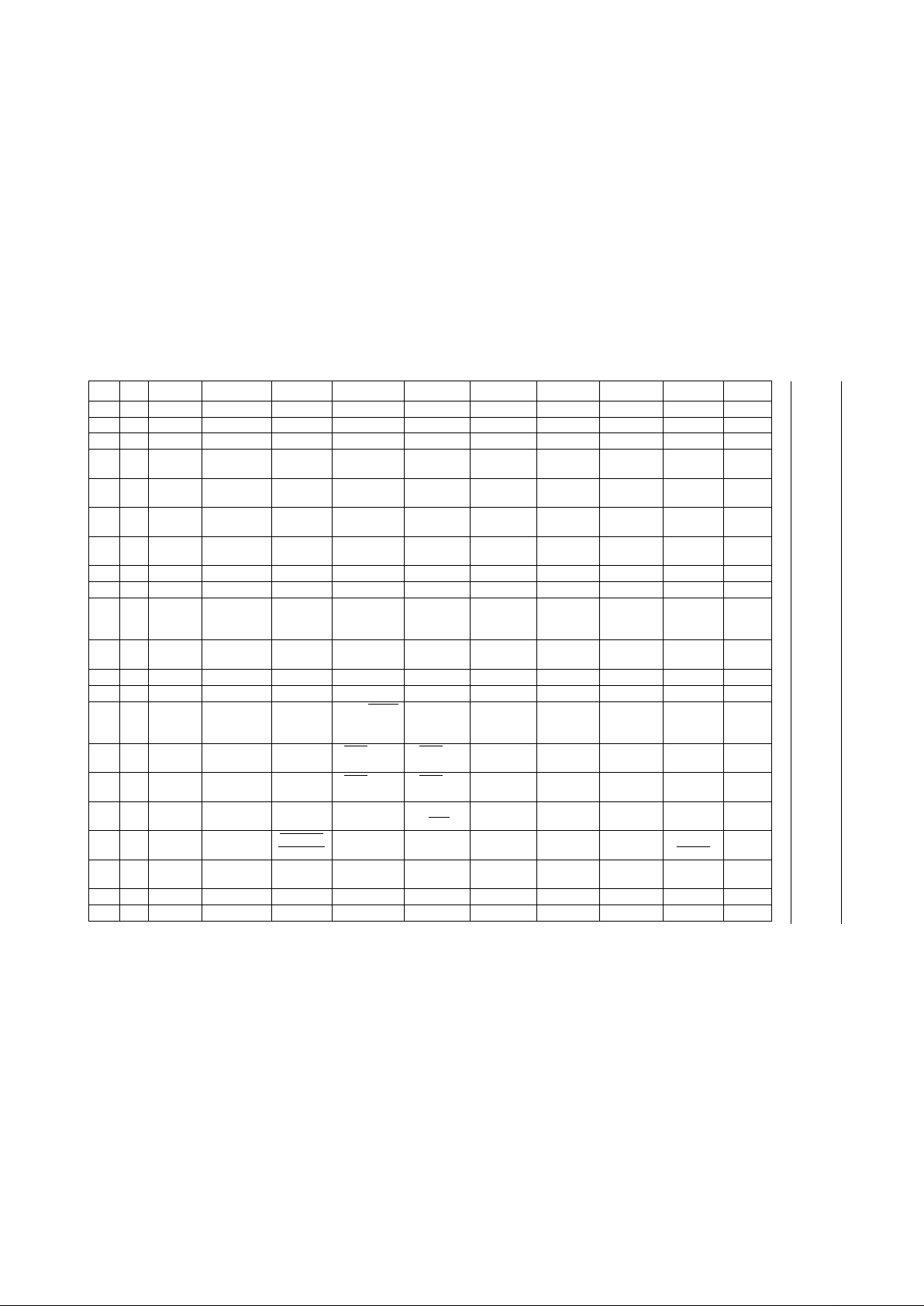
ADD R/W NAMES 7 6 5 4 3 2 1 0 RESET
80H R/W P0 P07 P06 P05 P04 P03 P02 P01 P00 FFH
81H R/W SP SP7 SP6 SP5 SP4 SP3 SP2 SP1 SP0 07H
82H R/W DPL DPL7 DPL6 DPL5 DPL4 DPL3 DPL2 DPL1 DPL0 00H
83H R/W DPH DPH7 DPH6 DPH5 DPH4 DPH3 DPH2 DPH1 DPH0 00H
87H R/W PCON 0 ARD RFI WLE GF1 GF0 PD IDL 00H
88H R/W TCON TF1 TR1 TF0 TR0 IE1 IT1 IE0 IT0 00H
89H R/W TMOD GATE C/
TM1 M0GATEC/T M1 M0 00H
8AH R/W TL0 TL07 TL06 TL05 TL04 TL03 TL02 TL01 TL00 00H
8BH R/W TL1 TL17 TL16 TL15 TL14 TL13 TL12 TL11 TL10 00H
8CH R/W TH0 TH07 TH06 TH05 TH04 TH03 TH02 TH01 TH00 00H
8DH R/W TH1 TH17 TH16 TH15 TH14 TH13 TH12 TH11 TH10 00H
90H R/W P1 P17 P16 P15 P14 P13 P12 P11 P10 FFH
96H R/W P0CFGA P0CFGA7 P0CFGA6 P0CFGA5 P0CFGA4 P0CFGA3 P0CFGA2 P0CFGA1 P0CFGA0 FFH
97H R/W P0CFGB P0CFGB7 P0CFGB6 P0CFGB5 P0CFGB4 P0CFGB3 P0CFGB2 P0CFGB1 P0CFGB0 00H
98H R/W SADB 0 0 0 DC_COMP SAD3 SAD2 SAD1 SAD0 00H
9EH R/W P1CFGA P1CFGA7 P1CFGA6 P1CFGA5 P1CFGA4 P1CFGA3 P1CFGA2 P1CFGA1 P1CFGA0 FFH
9FH R/W P1CFGB P1CFGB7 P1CFGB6 P1CFGB5 P1CFGB4 P1CFGB3 P1CFGB2 P1CFGB1 P1CFGB0 00H
A0H R/W P2 P27 P26 P25 P24 P23 P22 P21 P20 FFH
A6H R/W P2CFGA P2CFGA7 P2CFGA6 P2CFGA5 P2CFGA4 P2CFGA3 P2CFGA2 P2CFGA1 P2CFGA0 FFH
A7H R/W P2CFGB P2CFGB7 P2CFGB6 P2CFGB5 P2CFGB4 P2CFGB3 P2CFGB2 P2CFGB1 P2CFGB0 00H
A8H R/W IE EA EBUSY ES2 − ET1 EX1 ET0 EX0 00H
B0H R/W P3 P37 P36 P35 P34 P33 P32 P31 P30 FFH
B2H R/W TXT18 NOT3 NOT2 NOT1 NOT0 0 0 BS1 BS0 00H
B3H R/W TXT19 TEN TC2 TC1 TC0 0 0 TS1 TS0 00H
B4H R/W TXT20 0 0 0 0 OSD LANG
ENABLE
OSD LAN2 OSD LAN1 OSD LAN0 00H
1999 Oct 27 15
Philips Semiconductors Preliminary specification
Standard TV microcontrollers with
On-Screen Display (OSD)
SAA55xx
This text is here in white to force landscape pages to be rotated correctly when browsing through the pdf in the Acrobat reader.This text is here in
_white to force landscape pages to be rotated correctly when browsing through the pdf in the Acrobat reader.This text is here inThis text is here in
white to force landscape pages to be rotated correctly when browsing through the pdf in the Acrobat reader. white to force landscape pages to be ...
B5H R/W TXT21 0 0 0 0 I
2
C PORT 1 0 I2C PORT 0 0 02H
B6H R TXT22 GPF7 GPF6 0 GPF4 GPF3 0 GPF1 GPF0 XXH
B8H R/W IP 0 PBUSY PES2 PCC PT1 PX1 PT0 PX0 00H
B9H R/W TXT17 0 FORCE
ACQ1
FORCE
ACQ0
FORCE
DISP1
FORCE
DISP0
SCREEN
COL2
SCREEN
COL1
SCREEN
COL0
00H
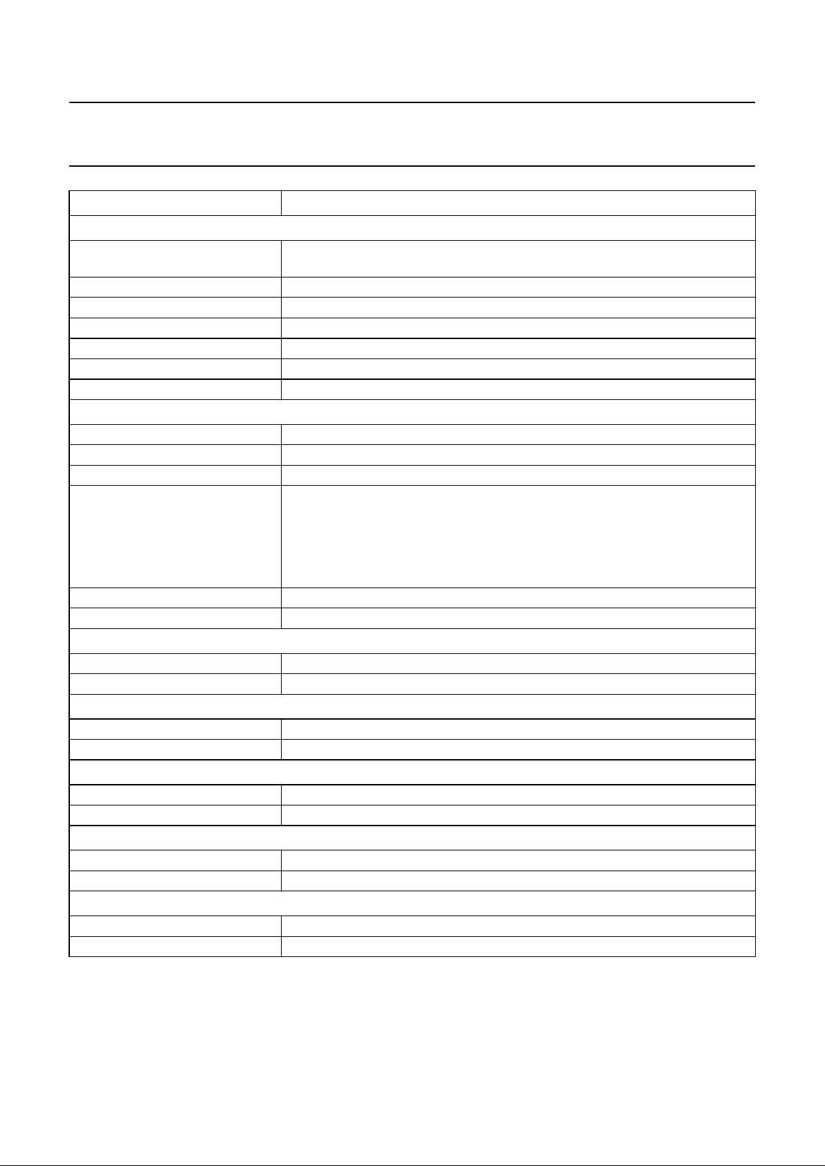
BAH R WSS1 0 0 0 WSS<3:0>
ERROR
WSS3 WSS2 WSS1 WSS0 00H
BBH R WSS2 0 0 0 WSS<7:4>
ERROR
WSS7 WSS6 WSS5 WSS4 00H
BCH R WSS3 WSS<13:11>
ERROR
WSS13 WSS12 WSS11 WSS<10:8>
ERROR
WSS10 WSS9 WSS8 00H
BEH R/W P3CFGA 1 1 1 P3CFGA4 P3CFGA3 P3CFGA2 P3CFGA1 P3CFGA0 FFH
BFH R/W P3CFGB 0 0 0 P3CFGB4 P3CFGB3 P3CFGB2 P3CFGB1 P3CFGB0 00H
C0H R/W TXT0 X24 POSN DISPLAY
X24
AUTO
FRAME
DISABLE
HEADER
ROLL
DISPLAY
STATUS
ROW ONLY
DISABLE
FRAME
VPS ON INV ON 00H
C1H R/W TXT1 EXT PKT
OFF
8-BIT ACQ OFF X26 OFF FULL FIELD FIELD
POLARITYHPOLARITYVPOLARITY
00H
C2H R/W TXT2 ACQ BANK REQ3 REQ2 REQ1 REQ0 SC2 SC1 SC0 00H
C3H W TXT3 −− −PRD4 PRD3 PRD2 PRD1 PRD0 00H
C4H R/W TXT4 OSD BANK
ENABLE
QUAD
WIDTH
ENABLE
EAST/
WEST DISABLE
DOUBLE
HEIGHT
B MESH
ENABLE
C MESH
ENABLE
TRANS
ENABLE
SHADOW
ENABLE
00H
C5H R/W TXT5 BKGND OUT BKGND IN
COR OUT COR IN TEXT OUT TEXT IN PICTURE
ON OUT
PICTURE
ON IN
03H
C6H R/W TXT6 BKGND OUT BKGND IN
COR OUT COR IN TEXT OUT TEXT IN PICTURE
ON OUT
PICTURE
ON IN
03H
C7H R/W TXT7 STATUS
ROW TOP
CURSORONREVEAL BOTTOM
/
TOP
DOUBLE
HEIGHT
BOX ON 24 BOX ON
1 − 23
BOX ON 0 00H
C8H R/W TXT8 (reserved)
0
FLICKER
STOP ON
(reserved)0DISABLE
SPANISH
PKT 26
RECEIVED
WSS
RECEIVED
WSS ON CVBS1/
CVBS0
00H
C9H R/W TXT9 CURSOR
FREEZE
CLEAR
MEMORY
A0 R4 R3 R2 R1 R0 00H
CAH R/W TXT10 0 0 C5 C4 C3 C2 C1 C0 00H
CBH R/W TXT11 D7 D6 D5 D4 D3 D2 D1 D0 00H
ADD R/W NAMES 7 6 5 4 3 2 1 0 RESET

1999 Oct 27 16
Philips Semiconductors Preliminary specification
Standard TV microcontrollers with
On-Screen Display (OSD)
SAA55xx
This text is here in white to force landscape pages to be rotated correctly when browsing through the pdf in the Acrobat reader.This text is here in
_white to force landscape pages to be rotated correctly when browsing through the pdf in the Acrobat reader.This text is here inThis text is here in
white to force landscape pages to be rotated correctly when browsing through the pdf in the Acrobat reader. white to force landscape pages to be ...
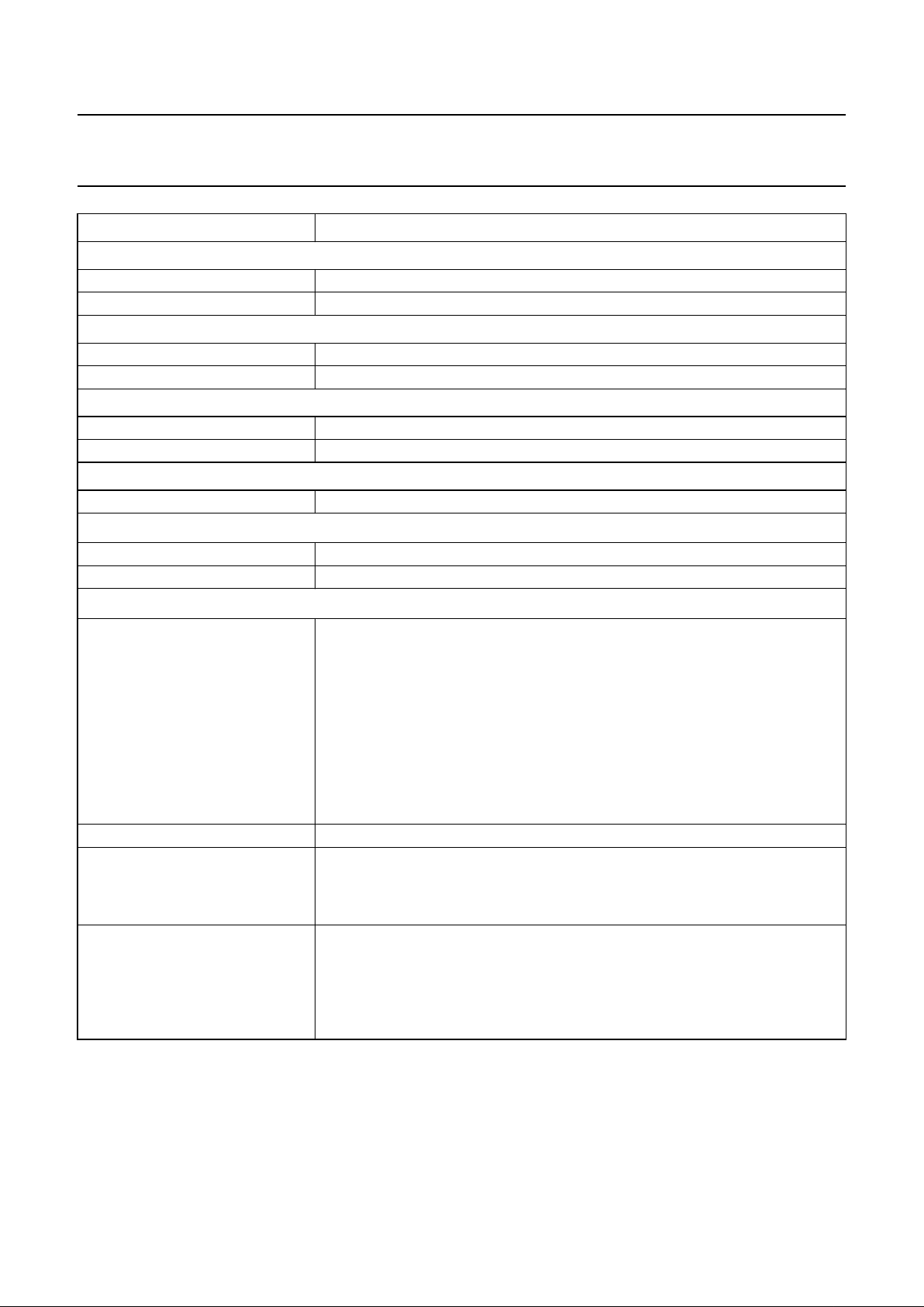
CCH R TXT12 525/
625
SYNC
SPANISH ROM VER3 ROM VER2 ROM VER1 ROM VER0 1 VIDEO
SIGNAL
QUALITY
XXXX
XX1X
CDH R/W TXT14 0 0 0 − PAGE3 PAGE2 PAGE1 PAGE0 00H
CEH R/W TXT15 0 0 0 − BLOCK3 BLOCK2 BLOCK1 BLOCK0 00H
D0H R/W PSW C AC F0 RS1 RS0 OV − P 00H
D2H R/W TDACL TD7 TD6 TD5 TD4 TD3 TD2 TD1 TD0 00H
D3H R/W TDACH TPWE 1 TD13 TD12 TD11 TD10 TD9 TD8 40H
D4H R/W PWM7 PW7E 1 PW7V5 PW7V4 PW7V3 PW7V2 PW7V1 PW7V0 40H
D5H R/W PWM0 PW0E 1 PW0V5 PW0V4 PW0V3 PW0V2 PW0V1 PW0V0 40H
D6H R/W PWM1 PW1E 1 PW1V5 PW1V4 PW1V3 PW1V2 PW1V1 PW1V0 40H
D8H R/W S1CON CR2 ENSI STA STO SI AA CR1 CR0 00H
D9H R S1STA STAT4 STAT3 STAT2 STAT1 STAT0 0 0 0 F8H
DAH R/W S1DAT DAT7 DAT6 DAT5 DAT4 DAT3 DAT2 DAT1 DAT0 00H
DBH R/W S1ADR ADR6 ADR5 ADR4 ADR3 ADR2 ADR1 ADR0 GC 00H
DCH R/W PWM3 PW3E 1 PW3V5 PW3V4 PW3V3 PW3V2 PW3V1 PW3V0 40H
DDH R/W PWM4 PW4E 1 PW4V5 PW4V4 PW4V3 PW4V2 PW4V1 PW4V0 40H
DEH R/W PWM5 PW5E 1 PW5V5 PW5V4 PW5V3 PW5V2 PW5V1 PW5V0 40H
DFH R/W PWM6 PW6E 1 PW6V5 PW6V4 PW6V3 PW6V2 PW6V1 PW6V0 40H
E0H R/W ACC ACC7 ACC6 ACC5 ACC4 ACC3 ACC2 ACC1 ACC0 00H
E4H R/W PWM2 PW2E 1 PW2V5 PW2V4 PW2V3 PW2V2 PW2V1 PW2V0 40H
E8H R/W SAD VHI CH1 CH0 ST SAD7 SAD6 SAD5 SAD4 00H
F0H R/W B B7 B6 B5 B4 B3 B2 B1 B0 00H
F8H R/W TXT13 VPS
RECEIVED
PAGE
CLEARING
525 DISPLAY 525 TEXT 625 TEXT PKT 8/30 FASTEXT 0 XXXX
XXX0
FAH R/W XRAMP XRAMP7 XRAMP6 XRAMP5 XRAMP4 XRAMP3 XRAMP2 XRAMP1 XRAMP0 00H
FBH R/W ROMBK STANDBY 0 0 0 0 0 (reserved)0(reserved)000H
FEH W WDTKEY WKEY7 WKEY6 WKEY5 WKEY4 WKEY3 WKEY2 WKEY1 WKEY0 00H
FFH R/W WDT WDV7 WDV6 WDV5 WDV4 WDV3 WDV2 WDV1 WDV0 00H
ADD R/W NAMES 7 6 5 4 3 2 1 0 RESET

1999 Oct 27 17
Philips Semiconductors Preliminary specification
Standard TV microcontrollers with
On-Screen Display (OSD)
SAA55xx
Table 3 SFR bit description
BIT FUNCTION
Accumulator (ACC)
ACC7 to ACC0 accumulator value
B Register (B)
B7 to B0 B register value
Data Pointer High byte (DPH)
DPH7 to DPH0 data pointer high byte, used with DPL to address auxiliary memory
Data Pointer Low byte (DPL)
DPL7 to DPL0 data pointer low byte, used with DPH to address auxiliary memory
Interrupt Enable Register (IE)
EA disable all interrupts (logic 0), or use individual interrupt enable bits (logic 1)
EBUSY enable BUSY interrupt
ES2 enable I
2
C-bus interrupt
ET1 enable Timer 1 interrupt
EX1 enable external interrupt 1
ET0 enable Timer 0 interrupt
EX0 enable external interrupt 0
Interrupt Priority Register (IP)
PBUSY priority EBUSY interrupt
PES2 priority ES2 interrupt
PCC priority ECC interrupt
PT1 priority Timer 1 interrupt
PX1 priority external interrupt 1
PT0 priority Timer 0 interrupt
PX0 priority external interrupt 0
Port 0 (P0)
P07 to P00 Port 0 I/O register connected to external pins
Port 1 (P1)
P17 to P10 Port 1 I/O register connected to external pins
Port 2 (P2)
P27 to P20 Port 2 I/O register connected to external pins
Port 3 (P3)
P37 to P30 Port 3 I/O register connected to external pins; P37 to P35 are only available with
the LQFP100 package

1999 Oct 27 18
Philips Semiconductors Preliminary specification
Standard TV microcontrollers with
On-Screen Display (OSD)
SAA55xx
Port 0 Configuration A (P0CFGA) and Port 0 Configuration B (P0CFGB)
P0CFGA<7:0> and P0CFGB<7:0> These two registers are used to configure Port 0 pins. For example, the
configuration of Port 0 pin 3 is controlled by setting bit 3 in both P0CFGA and
P0CFGB. P0CFGB<x>/P0CFGA<x>:
00 = P0.x in open-drain configuration
01 = P0.x in quasi-bidirectional configuration
10 = P0.x in high-impedance configuration
11 = P0.x in push-pull configuration
Port 1 Configuration A (P1CFGA) and Port 1 Configuration B (P1CFGB)
P1CFGA<7:0> and P1CFGB<7:0> These two registers are used to configure Port 1 pins. For example, the
configuration of Port 1 pin 3 is controlled by setting bit 3 in both P1CFGA and
P1CFGB. P1CFGB<x>/P1CFGA<x>:
00 = P1.x in open-drain configuration
01 = P1.x in quasi-bidirectional configuration
10 = P1.x in high-impedance configuration
11 = P1.x in push-pull configuration
Port 2 Configuration A (P2CFGA) and Port 2 Configuration B (P2CFGB)
P2CFGA<7:0> and P2CFGB<7:0> These two registers are used to configure Port 2 pins. For example, the
configuration of Port 2 pin 3 is controlled by setting bit 3 in both P2CFGA and
P2CFGB. P2CFGB<x>/P2CFGA<x>:
00 = P2.x in open-drain configuration
01 = P2.x in quasi-bidirectional configuration
10 = P2.x in high-impedance configuration
11 = P2.x in push-pull configuration
Port 3 Configuration A (P3CFGA) and Port 3 Configuration B (P3CFGB)
P3CFGA<7:0> and P3CFGB<7:0> These two registers are used to configure Port 3 pins. For example, the
configuration of Port 3 pin 3 is controlled by setting bit 3 in both P3CFGA and
P3CFGB. P3CFGB<x>/P3CFGA<x>:
00 = P3.x in open-drain configuration
01 = P3.x in quasi-bidirectional configuration
10 = P3.x in high-impedance configuration
11 = P3.x in push-pull configuration
BIT FUNCTION
1999 Oct 27 19
Philips Semiconductors Preliminary specification
Standard TV microcontrollers with
On-Screen Display (OSD)
SAA55xx
Power Control Register (PCON)
ARD auxiliary RAM disable bit, all MOVX instructions access the external data
memory
RFI disable ALE during internal access to reduce radio frequency interference
WLE Watchdog Timer enable
GF1 general purpose flag 1
GF0 general purpose flag 0
PD Power-down mode activation bit
IDL Idle mode activation bit
Program Status Word (PSW)
C carry bit
AC auxiliary carry bit
F0 flag 0
RS1 to RS0 register bank selector bits RS<1:0>:
00 = Bank 0 (00H to 07H)
01 = Bank 1 (08H to 0FH)
10 = Bank 2 (10H to 17H)
11 = Bank 3 (18H to 1FH)
OV overflow flag
P parity bit
Pulse Width Modulator 0 Control Register (PWM0)
PW0E activate this PWM and take control of respective port pin (logic 1)
PW0V5 to PW0V0 pulse width modulator high time
Pulse Width Modulator 1 Control Register (PWM1)
PW1E activate this PWM (logic 1)
PW1V5 to PW1V0 pulse width modulator high time
Pulse Width Modulator 2 Control Register (PWM2)
PW2E activate this PWM (logic 1)
PW2V5 to PW2V0 pulse width modulator high time
Pulse Width Modulator 3 Control Register (PWM3)
PW3E activate this PWM (logic 1)
PW3V5 to PW3V0 pulse width modulator high time
Pulse Width Modulator 4 Control Register (PWM4)
PW4E activate this PWM (logic 1)
PW4V5 to PW4V0 pulse width modulator high time
BIT FUNCTION
1999 Oct 27 20
Philips Semiconductors Preliminary specification
Standard TV microcontrollers with
On-Screen Display (OSD)
SAA55xx
Pulse Width Modulator 5 Control Register (PWM5)
PW5E activate this PWM (logic 1)
PW5V5 to PW5V0 pulse width modulator high time
Pulse Width Modulator 6 Control Register (PWM6)
PW6E activate this PWM (logic 1)
PW6V5 to PW6V0 pulse width modulator high time
Pulse Width Modulator 7 Control Register (PWM7)
PW7E activate this PWM (logic 1)
PW7V5 to PW7V0 pulse width modulator high time
ROM Bank (ROMBK)
STANDBY standby activation bit
I
2
C-bus Slave Address Register (S1ADR)
ADR6 to ADR0 I
2
C-bus slave address to which the device will respond
GC enable I
2
C-bus general call address (logic 1)
I
2
C-bus Control Register (S1CON)
CR2 to CR0 clock rate bits; CR<2:0>:
000 = 100 kHz bit rate
001 = 3.75 kHz bit rate
010 = 150 kHz bit rate
011 = 200 kHz bit rate
100 = 25 kHz bit rate
101 = 1.875 kHz bit rate
110 = 37.5 kHz bit rate
111 = 50 kHz bit rate
ENSI enable I
2
C-bus interface (logic 1)
STA START flag. When this bit is set in slave mode, the hardware checks the I
2
C-bus
and generates a START condition if the bus is free or after the bus becomes free.
If the device operates in master mode it will generate a repeated START
condition.
STO STOP flag. If this bit is set in a master mode a STOP condition is generated. A
STOP condition detected on the I
2
C-bus clears this bit. This bit may also be set
in slave mode in order to recover from an error condition. In this case no STOP
condition is generated to the I2C-bus, but the hardware releases the SDA and
SCL lines and switches to the not selected receiver mode. The STOP flag is
cleared by the hardware.
BIT FUNCTION

1999 Oct 27 21
Philips Semiconductors Preliminary specification
Standard TV microcontrollers with
On-Screen Display (OSD)
SAA55xx
SI Serial Interrupt flag. This flag is set and an interrupt request is generated, after
any of the following events occur:
• A START condition is generated in master mode
• The own slave address has been received during AA = 1
• The general call address has been received while S1ADR.GC and AA = 1
• Adatabytehasbeenreceivedortransmittedinmastermode(evenifarbitration
is lost)
• A data byte has been received or transmitted as selected slave
• A STOP or START condition is received as selected slave receiver or
transmitter.While the SI flag is set, SCL remains LOW and the serial transferis
suspended. SI must be reset by software.
AA Assert Acknowledge flag. When this bit is set, an acknowledge is returned
after any one of the following conditions:
• Own slave address is received
• General call address is received (S1ADR.GC = 1)
• A data byte is received, while the device is programmed to be a master receiver
• A data byte is received, while the device is selected slave receiver.
When the bit is reset, no acknowledge is returned. Consequently, no interrupt is
requested when the own address or general call address is received.
I
2
C-bus Data Register (S1DAT)
DAT7 to DAT0 I
2
C-bus data
I
2
C-bus Status Register (S1STA)
STAT4 to STAT0 I
2
C-bus interface status
Software ADC Register (SAD)
VHI analog input voltage greater than DAC voltage (logic 1)
CH1 to CH0 ADC input channel select bits; CH<1:0>:
00 = ADC3
01 = ADC0
10 = ADC1
11 = ADC2
ST
(1)
initiate voltage comparison between ADC input channel and SAD value
SAD7 to SAD4 4 MSBs of DAC input word
Software ADC Control Register (SADB)
DC_COMP enable DC comparator mode (logic 1)
SAD3 to SAD0 4 LSBs of SAD value
Stack Pointer (SP)
SP7 to SP0 stack pointer value
BIT FUNCTION

1999 Oct 27 22
Philips Semiconductors Preliminary specification
Standard TV microcontrollers with
On-Screen Display (OSD)
SAA55xx
Timer/Counter Control Register (TCON)
TF1 Timer 1 overflow flag. Set by hardware on timer/counter overflow. Cleared by
hardware when processor vectors to interrupt routine.
TR1 Timer 1 run control bit. Set/cleared by software to turn timer/counter on/off.
TF0 Timer 0 overflow flag. Set by hardware on timer/counter overflow. Cleared by
hardware when processor vectors to interrupt routine.
TR0 Timer 0 run control bit. Set/cleared by software to turn timer/counter on/off.
IE1 Interrupt 1 Edge flag. Both edges generate flag. Set by hardware when external
interrupt edge detected. Cleared by hardware when interrupt processed.
IT1 Interrupt 1 type control bit. Set/cleared by software to specify edge/LOW level
triggered external interrupts.
IE0 Interrupt 0 Edge l flag. Set by hardware when external interrupt edge detected.
Cleared by hardware when interrupt processed.
IT0 Interrupt 0 type flag. Set/cleared by software to specify falling edge/LOW level
triggered external interrupts.
14-bit PWM MSB Register (TDACH)
TPWE activate this 14-bit PWM (logic 1)
TD13 to TD8 6 MSBs of 14-bit number to be output by the 14-bit PWM
14-bit PWM LSB Register (TDACL)
TD7 to TD0 8 LSBs of 14-bit number to be output by the 14-bit PWM
Timer 0 High byte (TH0)
TH07 to TH00 8 MSBs of Timer 0 16-bit counter
Timer 1 High byte (TH1)
TH17 to TH10 8 MSBs of Timer 1 16-bit counter
Timer 0 Low byte (TL0)
TL07 to TL00 8 LSBs of Timer 0 16-bit counter
Timer 1 Low byte (TL1)
TL17 to TL10 8 LSBs of Timer 1 16-bit counter
Timer/Counter Mode Control (TMOD)
GATE gating control Timer/Counter 1
C/
T Counter/Timer 1 selector
M1 to M0 mode control bits timer/counter 1; M<1:0>:
00 = 8-bit timer or 8-bit counter with divide-by-32 prescaler
01 = 16-bit time interval or event counter
10 = 8-bit time interval or event counter with automatic reload upon overflow;
reload value stored in TH1
11 = stopped
GATE Gating control Timer/Counter 0
C/
T Counter/Timer 0 selector
BIT FUNCTION

1999 Oct 27 23
Philips Semiconductors Preliminary specification
Standard TV microcontrollers with
On-Screen Display (OSD)
SAA55xx
M1 to M0 mode control bits timer/counter 0; M<1:0>:
00 = 8-bit timer or 8-bit counter with divide-by-32 prescaler
01 = 16-bit time interval or event counter
10 = 8-bit time interval or event counter with automatic reload upon overflow;
reload value stored in TH0
11 = one 8-bit time interval or event counter and one 8-bit time interval counter
Text Register 0 (TXT0)
X24 POSN store packet 24 in extension packet memory (logic 0) or page memory (logic 1)
DISPLAY X24 display X24 from page memory (logic 0) or extension packet memory (logic 1)
AUTO FRAME FRAME output switched off automatically if any video displayed (logic 1)
DISABLE HEADER ROLL disable writing of rolling headers and time into memory (logic 1)
DISPLAY STATUS ROW ONLY display row 24 only (logic 1)
DISABLE FRAME FRAME output always LOW (logic 1)
VPS ON enable capture of VPS data (logic 1)
INV ON enable capture of inventory page in block 8 (logic 1)
Text Register 1 (TXT1)
EXT PKT OFF disable acquisition of extension packets (logic 1)
8-BIT disable checking of packets 0 to 24 written into memory (logic 1)
ACQ OFF disable writing of data into Display memory (logic 1)
X26 OFF disable automatic processing of X/26 data (logic 1)
FULL FIELD acquire data on any TV line (logic 1)
FIELD POLARITY VSYNC pulse in second half of line during even field (logic 1)
H POLARITY HSYNC reference edge is negative going (logic 1)
V POLARITY VSYNC reference edge is negative going (logic 1)
Text Register 2 (TXT2)
ACQ BANK select acquisition Bank 1 (logic 1)
REQ3 to REQ0 page request
SC2 to SC0 start column of page request
Text Register 3 (TXT3)
PRD4 to PRD0 page request data
Text Register 4 (TXT4)
OSD BANK ENABLE alternate OSD location available via graphic attribute, additional 32 locations
(logic 1)
QUAD WIDTH ENABLE enable display of quadruple width characters (logic 1)
EAST/
WEST eastern language selection of character codes A0H to FFH (logic 1)
DISABLE DOUBLE HEIGHT disable normal decoding of double height characters (logic 1)
B MESH ENABLE enable meshing of black background (logic 1)
C MESH ENABLE enable meshing of coloured background (logic 1)
TRANS ENABLE display black background as video (logic 1)
SHADOW ENABLE display shadow/fringe (default SE black) (logic 1)
BIT FUNCTION

1999 Oct 27 24
Philips Semiconductors Preliminary specification
Standard TV microcontrollers with
On-Screen Display (OSD)
SAA55xx
Text Register 5 (TXT5)
BKGND OUT background colour displayed outside teletext boxes (logic 1)
BKGND IN background colour displayed inside teletext boxes (logic 1)
COR OUT COR active outside teletext and OSD boxes (logic 1)
COR IN COR active inside teletext and OSD boxes (logic 1)
TEXT OUT text displayed outside teletext boxes (logic 1)
TEXT IN text displayed inside teletext boxes (logic 1)
PICTURE ON OUT video displayed outside teletext boxes (logic 1)
PICTURE ON IN video displayed inside teletext boxes (logic 1)
Text Register 6 (TXT6)
BKGND OUT background colour displayed outside teletext boxes (logic 1)
BKGND IN background colour displayed inside teletext boxes (logic 1)
COR OUT COR active outside teletext and OSD boxes (logic 1)
COR IN COR active inside teletext and OSD boxes (logic 1)
TEXT OUT text displayed outside teletext boxes (logic 1)
TEXT IN text displayed inside teletext boxes (logic 1)
PICTURE ON OUT video displayed outside teletext boxes (logic 1)
PICTURE ON IN video displayed inside teletext boxes (logic 1)
Text Register 7 (TXT7)
STATUS ROW TOP display memory row 24 information above teletext page (on display row 0)
(logic 1)
CURSOR ON display cursor at position given by TXT9 and TXT10 (logic 1)
REVEAL display characters in area with conceal attribute set (logic 1)
BOTTOM/
TOP display memory rows 12 to 23 when DOUBLE HEIGHT height bit is set (logic 1)
DOUBLE HEIGHT display each character as twice normal height (logic 1)
BOX ON 24 enable display of teletext boxes in memory row 24 (logic 1)
BOX ON 1 to 23 enable display of teletext boxes in memory row 1 to 23 (logic 1)
BOX ON 0 enable display of teletext boxes in memory row 0 (logic 1)
Text Register 8 (TXT8)
FLICKER STOP ON disable ‘Flicker Stopper’ circuitry (logic 1)
DISABLE SPANISH disable special treatment of Spanish packet 26 characters (logic 1)
PKT 26 RECEIVED
(2)
packet 26 data has been processed (logic 1)
WSS RECEIVED
(2)
WSS data has been processed (logic 1)
WSS ON enable acquisition of WSS data (logic 1)
CVBS1/
CVBS0 select CVBS1 as source for device (logic 1)
BIT FUNCTION
 Loading...