

Philips SAA5290 Service Manual

INTEGRATED CIRCUITS
DATA SH EET
SAA5290
One page Economy Teletext/TV
microcontroller
Preliminary specification
File under Integrated Circuits, IC02
Philips Semiconductors
February 1995

Philips Semiconductors Preliminary specification
One page Economy Teletext/TV
microcontroller
FEATURES
General
• Complete one page teletext decoder and TV
microcontroller in a single 52-pin package
• Eastern European, Western European and Turkish
language variants covered in one device
• Double size, double width and double height character
capability for On-Screen Display (OSD)
• Enhanced display features including meshing and
shadowing
• Separate display and acquisition timing for increased
flexibility
• Minimum peripheral component count
• 525 line and 625 line display synchronization
• Standby mode through power-down of teletext and
analog hardware.
Microcontroller
• 16 kbytes masked ROM (16 kbytes EEPROM variant for
product development)
• 256 bytes of on-chip RAM
• Six 6-bit Pulse Width Modulators (PWM) and one 14-bit
precision PWM
• 4-bit Digital-to-Analog Converter (DAC) and comparator
with a 3-input multiplexer allowing implementation of 3
Analog-to-Digital Converters (ADC) in software
• 2 high current (10 mA) open-drain outputs
• Interrupt logic 0 triggered on rising and falling edges,
providing pulse-width measurement for remote control
decoding
2
• Master and slave bit-level I
C-bus hardware.
SAA5290
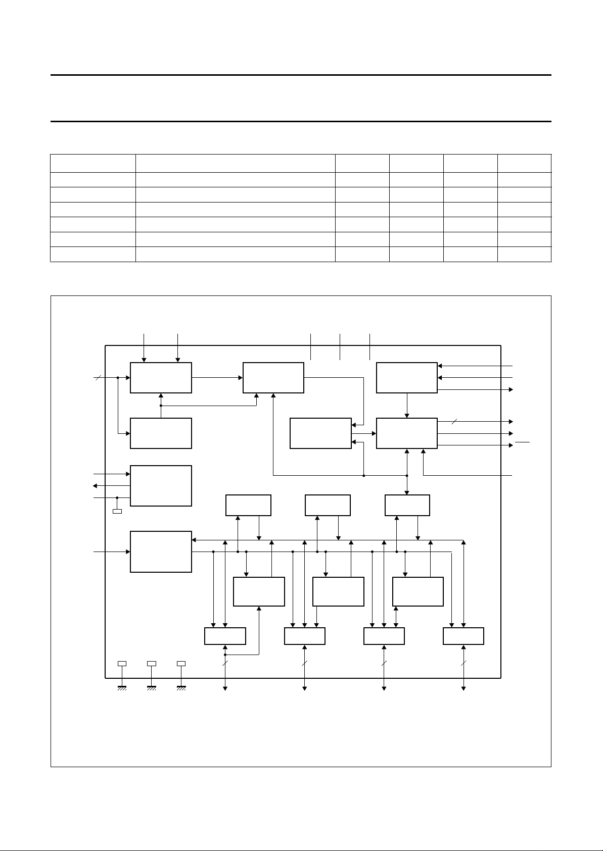
DESCRIPTION
The SAA5290 is a single-chip one page teletext decoder
and television control microcontroller. The device will
decode 625-line based World System Teletext
transmissions and provides television control functions
and On-Screen Display (OSD) functions.
The teletext decoder hardware is a derivative of the
SAA5254 (IVT1.1X), and the TV control functionality
provided by an on-chip industrial standard 80C51
microcontroller. A single-page static RAM is included
on-board providing a complete one page teletext decoder
and OSD memory.
The SAA5290 is available as a mask-programmed ROM
version. An EEPROM version is also available for product
development. Both versions are available in an SDIP52
package.
ORDERING INFORMATION
TYPE NUMBER MEMORY
SAA5290ZP/nnn
SAA5290ZP/NVI
Notes
1. nnn is a three-digit number referencing the microcontroller program ROM mask.
2. I is a digit number referring to the language variant of the SAA5290ZP/NV.
February 1995 2
(1)
(2)
ROM SDIP52 plastic shrink dual in-line package; 52 leads (600 mil) SOT247-1
EEPROM SDIP52 plastic shrink dual in-line package; 52 leads (600 mil) SOT247-1
NAME DESCRIPTION VERSION
PACKAGE
Philips Semiconductors Preliminary specification
One page Economy Teletext/TV
SAA5290
microcontroller
QUICK REFERENCE DATA
SYMBOL PARAMETER MIN. TYP. MAX. UNIT
V
DD
I
DDM
I
DDA
I
DDT
f
xtal
T
amb
BLOCK DIAGRAM
handbook, full pagewidth
2
CVBS0
CVBS1
23, 24
supply voltage 4.5 5.0 5.5 V
microcontroller supply current − 25 40 mA
analog supply current − 35 50 mA
teletext supply current − 20 30 mA
crystal frequency − 12 − MHz
operating ambient temperature −20 − +70 °C
BLACK IREF
25
DATA SLICER
V
V
DDA
26
TELETEXT
ACQUISITION
38
DDT
V
DDM
44
39
DISPLAY
TIMING
37
VSYNC
36
HSYNC
27
FRAME
OSCIN
OSCOUT
OSCGND
RESET
41
42
40
43
V
SSD1
ACQUISITION
TIMING
OSCILLATOR
80C51
MICRO-
CONTROLLER
2813
SSD2
V
V
data
address
22
SSA
ADC0 to ADC2
SAA5290
16K x 8
ANALOG-TOCONVERTER
PORT 3
5
9 to 12, 30
P3.0 to P3.4/
ROM
DIGITAL
PAGE
RAM
256 x 8
MODULATOR
PORT 2
8
1 to 8
P2.0 to P2.7
PWM
RAM
PULSE
WIDTH
P1.0 to P1.7 / INT0,
INT1, T0, T1, SDA, SCL
INTERFACE
PORT 1
8
45 to 52
DISPLAY
TEXT
TIMER/
CTRS/ I C
2
3
34, 33, 32
PORT 0
8
14 to 21
P0.0 to P0.7
R, G, B
35
VDS
29
COR
31
RGBREF
MLC102
Fig.1 Block diagram.
February 1995 3
Philips Semiconductors Preliminary specification
One page Economy Teletext/TV
SAA5290
microcontroller
PINNING
SYMBOL PIN DESCRIPTION
P2.0/TPWM 1 PORT 2: 8-bit open-drain bidirectional port with alternative functions. P2.0/TPWM is the
P2.1/PWM0 2
P2.2/PWM1 3
P2.3/PWM2 4
P2.4/PWM3 5
P2.5/PWM4 6
P2.6/PWM5 7
P2.7 8
P3.0/ADC0 9 PORT 3: 5-bit open-drain bidirectional port with alternative functions. P3.0/ADC0 to
P3.1/ADC1 10
P3.2/ADC2 11
P3.3 12
P3.4 30
V
SSD1
P0.0 14 PORT 0: 8-bit open-drain bidirectional port. P0.5 and P0.6 have 10 mA current sinking
P0.1 15
P0.2 16
P0.3 17
P0.4 18
P0.5 19
P0.6 20
P0.7 21
V
SSA
CVBS0 23 Composite video input. A positive-going 1 V (peak-to-peak) input is required, connected
CVBS1 24
BLACK 25 Video black level storage input. This pin should be connected to V
IREF 26 Reference current input for analog circuits, connected to V
FRAME 27 De-interlace output synchronized with the VSYNC pulse to produce a non-interlaced
V
SSD2
COR 29 Open-drain, active LOW output which allows selective contrast reduction of the TV
RGBREF 31 DC input voltage to define the output HIGH level on the RGB pins.
B 32 Dot rate character output of the BLUE colour information.
G 33 Dot rate character output of the GREEN colour information.
R 34 Dot rate character output of the RED colour information.
VDS 35 Video/data switch push-pull output for dot rate fast blanking.
HSYNC 36 Horizontal sync dedicated input for a TTL-level version of the horizontal sync pulse. The
13 digital ground 1 for teletext and microcontroller circuits.
22 analog ground.
28 Digital ground 2.
output for the 14-bit high precision PWM. P2.1/PWM0 to P2.6/PWM5 are the outputs for
the 6-bit PWMs 0 to 5.
P3.2/ADC2 are the inputs for the software ADC facility.
capability at 0.5 V for direct drive of LEDs.
via a 100 nF capacitor.
via a 100 nF
SSA
capacitor.
via a 27 kΩ resistor.
SSA
display by adjustment of the vertical deflection currents.
picture to enhance a mixed mode display.
polarity of this pulse is programmable by register bit TXT1.H POLARITY.
February 1995 4
Philips Semiconductors Preliminary specification
One page Economy Teletext/TV
SAA5290
microcontroller
SYMBOL PIN DESCRIPTION
VSYNC 37 Vertical sync dedicated input for a TTL-level version of the vertical sync pulse. The
polarity of this pulse is programmable by register bit TXT1.V POLARITY.
V
DDA
V
DDT
OSCGND 40 Crystal oscillator ground.
OSCIN 41 12 MHz crystal oscillator input.
OSCOUT 42 12 MHz crystal oscillator output.
RESET 43 If the reset input is HIGH for 2 machine cycles (24 oscillator periods) while the oscillator
V
DDM
P1.0/INT1 45 PORT 1: 8-bit open-drain bidirectional port with alternative functions. P1.0/INT1 is
P1.1/T0 46
P1.2/INT0 47
P1.3/T1 48
P1.6/SCL 49
P1.7/SDA 50
P1.4 51
P1.5 52
38 +5 V analog power supply.
39 +5 V teletext power supply.
is running, the SAA5290 is reset. This pin should be connected to V
capacitor.
44 +5 V microcontroller power supply.
external interrupt 1 which can be triggered on the rising and falling edge of the pulse.
P1.1/T0 is the counter/timer 0. P1.2/INT0 is external interrupt 0. P1.3/T1 is the
counter/timer 1. P1.6/SCL is the serial clock input for I
data port for the I2C-bus.
via a 2.2 µF
DDM
2
C-bus. P1.7/SDA is the serial
February 1995 5
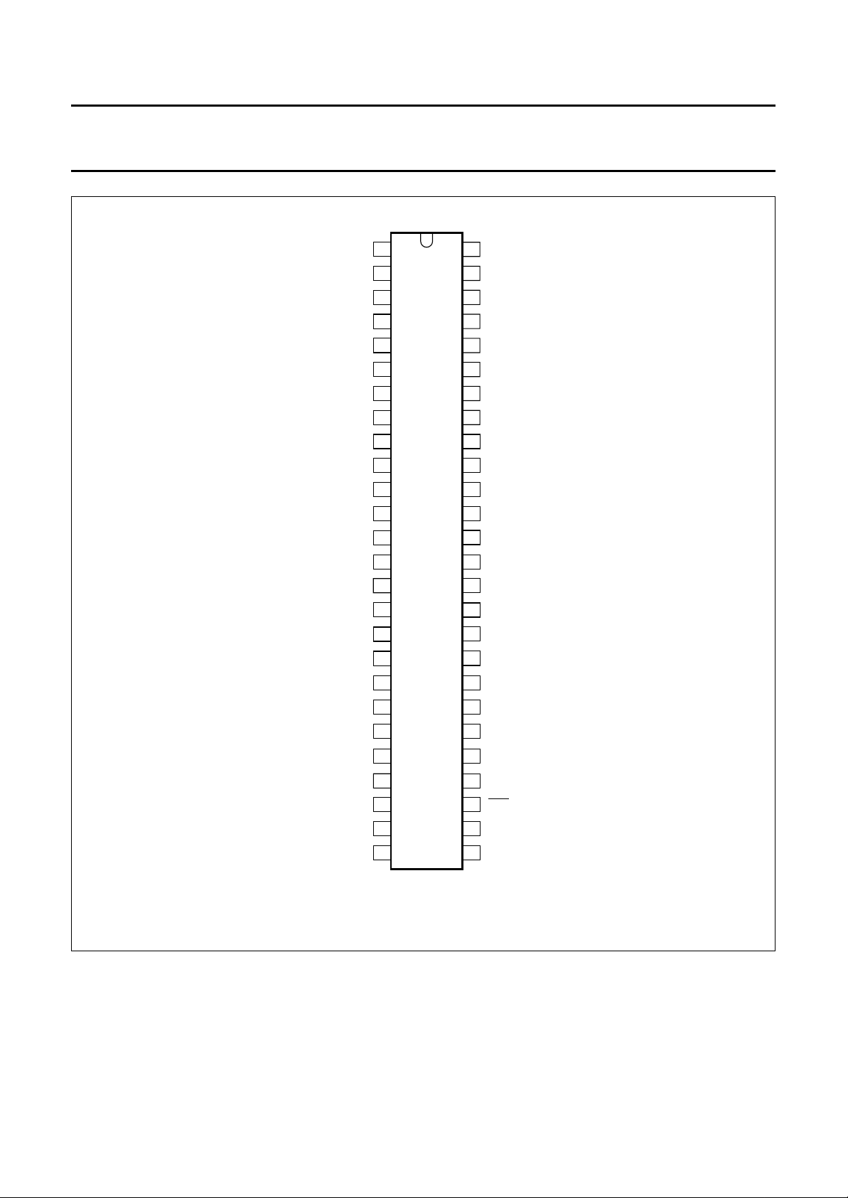
Philips Semiconductors Preliminary specification
One page Economy Teletext/TV
microcontroller
handbook, halfpage
P2.0/TPWM
P2.1/PWM0
P2.2/PWM1
P2.3/PWM2
P2.4/PWM3
P2.5/PWM4
P2.6/PWM5
P2.7
P3.0/ADC0
P3.1/ADC1
P3.2/ADC2
P3.3
V
SSD1
P0.0
P0.1
P0.2
P0.3
1
2
3
4
5
6
7
8
9
10
11
12
13
14
15
16
17
SAA5290
52
51
50
49
48
47
46
45
44
43
42
41
40
39
38
37
36
P1.5
P1.4
P1.7/SDA
P1.6/SCL
P1.3/T1
P1.2/INT0
P1.1/T0
P1.0/INT1
V
DDM
RESET
OSCOUT
OSCIN
OSCGND
V
DDT
V
DDA
VSYNC
HSYNC
SAA5290
18
P0.4
19
P0.5
20
P0.6
21
P0.7
V
22
SSA
IREF
23
24
25
26
MLC103
CVBS0
CVBS1
BLACK
Fig.2 Pin configuration.
35
34
33
32
31
30
29
28
27
VDS
R
G
B
RGBREF
P3.4
COR
V
SSD2
FRAME
February 1995 6
Philips Semiconductors Preliminary specification
One page Economy Teletext/TV
microcontroller
QUALITY AND RELIABILITY
This device will meet Philips Semiconductors General Quality Specification for Business group
Circuits SNW-FQ-611-Part E”
requirements are shown in Tables 1 to 4.
Group A
Table 1 Acceptance tests per lot
TEST REQUIREMENTS
Mechanical cumulative target: <80 ppm
Electrical cumulative target: <80 ppm
Group B
Table 2 Processability tests (by package family)
TEST REQUIREMENTS
Solderability <7% LTPD
Mechanical <15% LTPD
Solder heat resistance <15% LTPD
(see
“Quality Reference Handbook”
, order number 9398 510 63011). The principal
(1)
(1)
SAA5290
“Consumer Integrated
Group C
Table 3 Reliability tests (by process family)
TEST CONDITIONS REQUIREMENTS
Operational life 168 hours at Tj= 150 °C <1500 FPM; equivalent to
<100 FITS at Tj =70°C
Humidity life temperature, humidity, bias
<2000 FPM
1000 hours, 85 °C, 85% RH
(or equivalent test)
Temperature cycling performance T
stg(min)
to T
stg(max)
<2000 FPM
Table 4 Reliability tests (by device type)
TEST CONDITIONS REQUIREMENTS
ESD and latch-up ESD Human body model
<15% LTPD
2000 V, 100 pF, 1.5 kΩ
ESD Machine model
<15% LTPD
200 V, 200 pF, 0 Ω
latch-up 100 mA, 1.5 × V
DD
<15% LTPD
(absolute maximum)
Notes to Tables 1 to 4
1. ppm = fraction of defective devices, in parts per million.
LTPD = Lot Tolerance Percent Defective.
FPM = fraction of devices failing at test condition, in Failures Per Million.
FITS = Failures In Time Standard.
(1)
(1)
February 1995 7

Philips Semiconductors Preliminary specification
One page Economy Teletext/TV
SAA5290
microcontroller
LIMITING VALUES
In accordance with Absolute Maximum Rating System (IEC 134).
SYMBOL PARAMETER CONDITIONS MIN. MAX. UNIT
V
DD
V
I
V
O
I
O
I
IOK
∆V
SS
∆V
DD
T
amb
T
stg
Notes
1. This maximum value has an absolute maximum of 6.5 V independent of V
2. Except in standby mode.
supply voltage (all supplies) −0.3 +6.5 V
input voltage (any input) note 1 −0.3 VDD+ 0.5 V
output voltage (any output) note 1 −0.3 VDD+ 0.5 V
output current (each output) −±10 mA
DC input or output diode current −±20 mA
difference between V
difference between V
SSD
DDM
, V
and OSCGND −±0.1 V
SSA
, V
DDT
and V
DDA
note 2 −±0.1 V
operating ambient temperature −20 +70 °C
storage temperature −55 +125 °C
.
DD
CHARACTERISTICS
VDD=5V±10%; VSS=0V; T
= −20 to +70 °C; unless otherwise specified.
amb
SYMBOL PARAMETER CONDITIONS MIN. TYP. MAX. UNIT
Supplies
V
DD
I
DDM
I
DDA
I
DDT
supply voltage (VDD to VSS) 4.5 5.0 5.5 V
microcontroller supply current − 25 40 mA
analog supply current − 35 50 mA
teletext supply current − 20 30 mA
Digital inputs
RESET
V
IL
V
IH
I
LI
C
I
LOW level input voltage −0.3 − 0.2VDD− 0.1 V
HIGH level input voltage 0.7V
input leakage current VI= 0 to V
DD
−10 − +10 µA
DD
− VDD+ 0.3 V
input capacitance −−4pF
HSYNC AND VSYNC
V
thf
V
thr
V
HYS
C
I
switching threshold falling 0.2V
DD
switching threshold rising −−0.8V
hysteresis voltage − 0.33V
input capacitance −−4pF
−− V
V
− V
DD
DD
February 1995 8
Philips Semiconductors Preliminary specification
One page Economy Teletext/TV
SAA5290
microcontroller
SYMBOL PARAMETER CONDITIONS MIN. TYP. MAX. UNIT
Digital outputs
R, G AND B (note 1)
V
OL
V
OH
| output impedance −−150 Ω
|Z
O
C
L
I
O
t
r
t
f
COR (OPEN-DRAIN OUTPUT)
V
OH
V
OL
I
OL
C
L
VDS
V
OL
V
OH
C
L
t
r
t
f
R, G, B AND VDS
t
skew
FRAME
V
OH
V
OL
I
OL
C
L
LOW level output voltage IOL= 2 mA 0 − 0.2 V
HIGH level output voltage IOH= −2mA V
RGBREF
− 0.3
V
RGBREFVRGBREF
+ 0.4
V
load capacitance −−50 pF
DC output current −−−4mA
output rise time between 10% and 90%;
−−20 ns
CL=50pF
output fall time between 90% and 10%;
−−20 ns
CL=50pF
HIGH level pull-up output
−−VDDV
voltage
LOW level output voltage IOL= 2 mA 0 − 0.5 V
LOW level output current −−2mA
load capacitance −−25 pF
LOW level output voltage IOL= 1.6 mA 0 − 0.2 V
HIGH level output voltage IOH= −1.6 mA VDD− 0.3 − VDD+ 0.4 V
load capacitance −−50 pF
output rise time between 10% and 90%;
−−20 ns
CL=50pF
output fall time between 90% and 10%;
−−20 ns
CL=50pF
skew delay between any two
−−20 ns
pins
HIGH level output voltage IOL= 8 mA 0 − 0.5 V
LOW level output voltage IOL= −8mA VDD− 0.5 − V
DD
V
LOW level output current −8 − +8 mA
load capacitance −−100 pF
February 1995 9

Philips Semiconductors Preliminary specification
One page Economy Teletext/TV
SAA5290
microcontroller
SYMBOL PARAMETER CONDITIONS MIN. TYP. MAX. UNIT
Digital input/outputs
P0.0 TO P0.4, P0.7, P1.0 TO P1.5, P2.0 TO P2.7 AND P3.0 TO P3.5
V
IL
V
IH
C
I
V
OL
C
L
P0.5 AND P0.6
V
IL
V
IH
C
I
V
OL
C
L
P1.6 AND P1.7
V
IL
V
IH
C
I
V
OL
C
L
t
f
Analog inputs
LOW level input voltage −0.3 − 0.2VDD− 0.1 V
HIGH level input voltage 0.2VDD+ 0.9 − VDD+ 0.3 V
input capacitance −−4pF
LOW level output voltage IOL= 3.2 mA 0 − 0.45 V
load capacitance −−50 pF
LOW level input voltage −0.3 − 0.2VDD− 0.1 V
HIGH level input voltage 0.2VDD+ 0.9 − VDD+ 0.3 V
input capacitance −−4pF
LOW level output voltage IOL=10mA 0 − 0.45 V
load capacitance −−50 pF
LOW level input voltage −0.3 − +1.5 V
HIGH level input voltage 3.0 − VDD+ 0.3 V
input capacitance −−5pF
LOW level output voltage IOL= 3 mA 0 − 0.5 V
load capacitance −−400 pF
output fall time between 3 and 1 V −−200 ns
CVBS0
V
V
sync
vid(p-p)
AND CVBS1
sync voltage amplitude 0.1 0.3 0.6 V
video input voltage amplitude
0.7 1.0 1.4 V
(peak-to-peak value)
Z
source
V
IH
| input impedance 2.5 5.0 − kΩ
|Z
I
C
I
source impedance −−250 Ω
HIGH level input voltage 3.0 − VDD+ 0.3 V
input capacitance −−10 pF
IREF
R
gnd
resistor to ground − 27 − kΩ
RGBREF (note 1)
V
I
I
I
input voltage −0.3 − V
DD
DC input current −−12 mA
February 1995 10
V
 Loading...