

Philips SAA5284GP, SAA5284GP-M1 Datasheet
DATA SH EET
Objective specification
Supersedes data of 1997 Mar 03
File under Integrated Circuits, IC22
1998 Feb 05
INTEGRATED CIRCUITS
SAA5284
Multimedia video data acquisition
circuit

1998 Feb 05 2
Philips Semiconductors Objective specification
Multimedia video data acquisition circuit SAA5284
CONTENTS
1 FEATURES
2 GENERAL DESCRIPTION
3 QUICK REFERENCE DATA
4 ORDERING INFORMATION
5 MAIN FUNCTIONAL BLOCKS
6 BLOCK DIAGRAM
7 PINNING INFORMATION
7.1 Pinning
7.2 Pin description
8 FUNCTIONAL DESCRIPTION
8.1 Power supply strategy
8.2 Clocking strategy
8.3 Power-on reset
8.4 Analog switch
8.5 Analog video-to-data byte converter
8.6 Packet filtering
8.7 Packet buffer
8.8 FIFO
8.9 Host interface
8.10 Interrupt support
8.11 DMA support
8.12 I2C-bus interface
9 LIMITING VALUES
10 QUALITY & RELIABILITY
11 CHARACTERISTICS
12 TIMING
13 APPLICATION INFORMATION
13.1 Hardware application circuit for ISA card
13.2 Hardware application circuit for PCI application
13.3 Software application information
14 PACKAGE OUTLINE
15 SOLDERING
15.1 Introduction
15.2 Reflow soldering
15.3 Wave soldering
15.4 Repairing soldered joints
16 DEFINITIONS
17 LIFE SUPPORT APPLICATIONS
18 PURCHASE OF PHILIPS I2C COMPONENTS
1998 Feb 05 3
Philips Semiconductors Objective specification
Multimedia video data acquisition circuit SAA5284
1 FEATURES
• High performance multi-standard data slicer
• Intercast (Intel Corporation) compatible
• Teletext (WST, Chinese teletext) (625 lines)
• Teletext (US teletext, NABTS and MOJI) (525 lines)
• Wide Screen Signalling (WSS), Video Programming
Signal (VPS)
• Closed Caption (Europe, US)
• Data broadcast, PDC (packet 30 and 31)
• User programmable data format (programmable framing
code)
• 2 kbytes data cache on-chip to avoid data loss and
reduce host CPU overhead
• Filtering of packets 30 and 31 WST/NABTS
• Choice of clock frequencies, direct-in clock or crystal
oscillator
• Parallel interface, Motorola, Intel and digital video bus
• I
2
C-bus control
• Data transport by digital video bus
• Choice of programmable interrupt, DMA or polling
driven
• Data type selectable video line by video line, with
Vertical Blanking Interval and Full Field mode
• Single IC with few external components and small
footprint QFP44 package
• Optimized for EMC.
2 GENERAL DESCRIPTION
The SAA5284 is a Vertical Blanking Interval (VBI) and Full
Field (FF) video data acquisition device tailored for
application on PC add-in cards, PC mother-boards, set-top
boxes and as a SAA5250 replacement. The IC in
combination with a range of software modules will acquire
most existing formats of broadcast VBI and FF data.
These associated software modules are available under
licence. Scope is provided for acquiring some as yet
unspecified formats. The SAA5284 incorporates all the
data slicing, parallel interface, data filtering and control
logic. It is controlled either by a parallel interface or
I
2
C-bus. It can output ASCII VBI data as pixels on the
digital video bus where no parallel port is available. It is
available in a QFP44 package.
3 QUICK REFERENCE DATA
Note
1. Selectable: 12, 13.5, 15 or 16 MHz.
4 ORDERING INFORMATION
SYMBOL PARAMETER MIN. TYP. MAX. UNIT
V
DD
supply voltage 4.5 5.0 5.5 V
I
DD
supply current − 72 95 mA
V
sync(p-p)
sync voltage (peak-to-peak value) 0.1 0.3 0.6 V
V
i(CVBS)(p-p)
input voltage on pin CVBS0 and CVBS1
(peak-to-peak value)
0.7 1.0 1.4 V
f
xtal
crystal frequency; see note 1 − 12.0 − MHz
T
amb
operating ambient temperature −20 − +70 °C
TYPE NUMBER
PACKAGE
NAME DESCRIPTION VERSION
SAA5284GP QFP44 plastic quad flat package; 44 leads (lead length 2.35 mm);
body 14 × 14 × 2.2 mm
SOT205-1
1998 Feb 05 4
Philips Semiconductors Objective specification
Multimedia video data acquisition circuit SAA5284
5 MAIN FUNCTIONAL BLOCKS
1. Input clamp and sync separator
2. Analog-to-digital converter
3. Multi-standard data slicer and clock regenerator
4. Packet filtering; (8 and 4) Hamming correction
5. On-chip data cache
6. Line selectable data type
7. 12, 13.5, 15 and 16 MHz clock or oscillator options
8. FIFO access to data
9. Interrupt and DMA support
10. Multi-standard parallel interface
11. I
2
C-bus interface
12. Power-on reset.
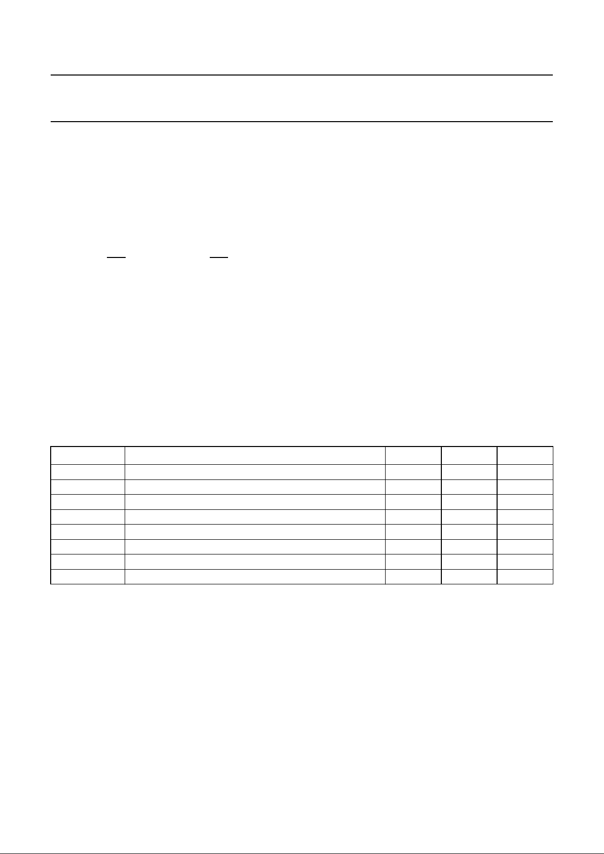
Figure 1 shows a block diagram of the SAA5284.
6 BLOCK DIAGRAM
Fig.1 Block diagram.
handbook, full pagewidth
MGG740
ANALOG
SWITCH
SAA5284
MULTI-STANDARD
HOST INTERFACE
I2C-BUS
INTERFACE
400 kHz
SLAVE
FIFO
PACKET BUFFER AND
FRONT END CONTROL
REGISTERS
PACKET
FILTERING (e.g.
WST packets
30/31)
ANALOG
VIDEO TO
DATA BYTE
CONVERTER
(DATA
DEMODULATOR)
OSCILLATOR
AND TIMING
OSCOUT OSCGND
OSCIN
PACKET BUFFER RAM
2 kbyte
(45 packets)
35
44
31
32
10
33 34424323938 36 37
11
3
SDA
SCL
4
5
30 to 28
20 to 27
WR
(1)
16
15
14
V
DDAVSSAVDDXVDDDVSSD3
RESET
17 6
41 40 1
VPOIN0 HREF
VPOIN1
LLC
LLC2
RD
(1)
DMACK
(1)
DMARQ
CVBS0
CVBS1
V
SSD1
V
SSD2
data path
control
13
12
789 18 19
I
REF
BLACK
8
3
D7 to D0
(1)
A2 to A0
(1)
RDY
(1)
SEL1
SEL0
INT
CS1
DENB
CS0
(1) Multi-functional pins, see Chapter 7.
1998 Feb 05 5
Philips Semiconductors Objective specification
Multimedia video data acquisition circuit SAA5284
7 PINNING INFORMATION
7.1 Pinning
7.2 Pin description
Table 1 QFP44 package
The IC has a total of 44 pins; many of these are multi-functional due to the multiple host block modes of operation.
SYMBOL PIN I/O DESCRIPTION
RESET 1 I reset IC
HREF 2 I video horizontal reference signal (digital video mode only)
SDA 3 I/O serial data port for I
2
C-bus, open-drain
SCL 4 I serial clock input for I2C-bus
DENB 5 O data enable bar (for external buffers)
V
DDX
6 − +5 V supply
OSCOUT 7 O oscillator output
OSCIN 8 I oscillator input
Fig.2 Pin configuration.
(1) Multi-functional pin.
handbook, full pagewidth
1
2
3
4
5
6
7
8
9
10
11
33
32
31
30
29
28
27
26
25
24
23
12
13
14
15
16
17
18
19
20
21
22
44
43
42
41
40
39
38
37
36
35
34
SAA5284
MGG739
WR
(1)
RDY
(1)
INT
A2
(1)
A0
(1)
D0
(1)
D1
(1)
D2
(1)
D3
(1)
D4
(1)
RESET
HREF
SDA
SCL
DENB
V
DDX
OSCIN
OSCGND
SEL1
A1
(1)
LLC2
LLC
V
DDD
V
SSD3
VPOIN1
VPOIN0
DMARQ
CS0
RD
(1)
CS1
DMACK
(1)
I
REF
CVBS1
CVBS0
V
DDA
V
SSA
V
SSD1
D7
(1)
D6
(1)
D5
(1)
BLACK
V
SSD2
OSCOUT
SEL0
1998 Feb 05 6
Philips Semiconductors Objective specification
Multimedia video data acquisition circuit SAA5284
Note
1. These pins have two functions, depending on the interface mode.
OSCGND 9 − oscillator ground
SEL0 10 I parallel interface format select 0
SEL1 11 I parallel interface format select 1
BLACK 12 I/O video black level storage; connected to V
SSA
via 100 nF capacitor
I
REF
13 I reference current input; connected to V
SSA
via 27 kΩ resistor
CVBS1 14 I analog composite video input 1
CVBS0 15 I analog composite video input 0
V
DDA
16 − analog +5 V supply
V
SSA
17 − analog ground supply
V
SSD1
18 I digital ground supply 1
V
SSD2
19 I digital ground supply 2
D7
(1)
20 I/O data bus 7/video data output 7
D6
(1)
21 I/O data bus 6/video data output 6
D5
(1)
22 I/O data bus 5/video data output 5
D4
(1)
23 I/O data bus 4/video data output 4
D3
(1)
24 I/O data bus 3/video data output 3
D2
(1)
25 I/O data bus 2/video data output 2
D1
(1)
26 I/O data bus 1/video data output 1
D0
(1)
27 I/O data bus 0/video data output 0
A0
(1)
28 I address input 0/video data input 7
A1
(1)
29 I address input 1/video data input 6
A2
(1)
30 I address input 2/video data input 5
INT 31 O interrupt request
RDY
(1)
32 O ready/DTACK (data acknowledge)/VBI, open-drain
WR
(1)
33 I Intel bus Write/Motorola bus R/W/video data input 4
RD
(1)
34 I Intel bus Read/Motorola bus LDS/video data input 3
CS0 35 I chip select 0; active LOW
DMARQ 36 O DMA request
DMACK
(1)
37 I DMA acknowledge/video data input 2
VPOIN0 38 I video data input 0
VPOIN1 39 I video data input 1
V
SSD3
40 − digital ground supply 3
V
DDD
41 − digital +5 V supply
LLC 42 I full rate digital video clock input
LLC2 43 I half rate digital video clock input
CS1 44 I chip select 1; active LOW
SYMBOL PIN I/O DESCRIPTION

1998 Feb 05 7
Philips Semiconductors Objective specification
Multimedia video data acquisition circuit SAA5284
8 FUNCTIONAL DESCRIPTION
8.1 Power supply strategy
There are three separate +5 V (V
DD
) connections to the IC:
1. V
DDA
supplies the critical noise-sensitive analog
front-end sections: ADC and sync separator, to reduce
interference from the rest of the front-end
2. V
DDX
supplies all sections which take standing DC
current
3. V
DDD
supplies the rest of the logic.
8.2 Clocking strategy
The master frequency reference for the IC is a
12, 13.5, 15 or 16 MHz crystal oscillator. The tolerance on
the clock frequency is 500 × 10
−6
(1.5 kHz). Further
specifications of the crystal are given in Table 2.
If preferred, an external 12, 13.5, 15 or 16 MHz (±1.5 kHz)
frequency source may be connected to OSCIN instead of
the crystal.
8.3 Power-on reset
The RESET pin should be held HIGH for a minimum of two
clock cycles. The reset signal is passed through a Schmitt
trigger internally.
Direct addressed registers (i.e. those addressed using the
A0 to A2 pins) are set to 00H after power-up. All other
register bits are assumed to be in random states after
power-up.
8.4 Analog switch
Register bit selection between two video sources.
8.5 Analog video-to-data byte converter
This section comprises a line and field sync separator, a
video clamp, an ADC and a custom adaptive digital filter
with DPLL based timing circuit.
The analog video-to-data byte converter is specifically
designed to overcome the most commonly found types of
distortion of a broadcast video signal. It is also fully
multi-standard. The data type to be demodulated is
programmable on a line-by-line basis using 4 register bits
per line for lines 2 to 23 (PAL numbering),
fields 1 and 2, and 4 further bits for all lines combined.
8.6 Packet filtering
If using a slow (e.g. 80C51) microcontroller, it is necessary
to reduce the amount of data acquired by SAA5284 before
downloading to the microcontroller to avoid it being
swamped by unwanted data. Packet filtering is available
for this purpose. A common use of this would be to acquire
only packet 8/30 in 625-line WST. The packet filter
includes optional (8, 4) Hamming correction.
8.7 Packet buffer
This is a 2 kbyte RAM which acts as a buffer for storing
received packets. The first 44 bytes are reserved for
control information. The rest of the RAM is divided into
44-byte rows (or packets), each holding the data received
on one incoming CVBS line. In the case of a WST packet
received, the data stored consists of a Magazine and
Row-Address Group (2 bytes), followed by the 40 bytes of
packet data. When data in other formats than WST is
received, this is stored in the packet buffer in the same
way. In each case, the data is preceded by two information
bytes which record on which line and field the packet was
received, and what the data type is.
8.8 FIFO
FIFO hardware is provided to manage the ‘read’ address
for the host processor, i.e. data is read repeatedly from the
same 8-bit port, and appears byte-serially in the order of
reception. The read address can be reset to the start of the
packet buffer (the first 44-byte packet), back to the start of
the current packet, or incremented to the start of the next
packet.
Table 2 Crystal characteristics
SYMBOL PARAMETER MIN. TYP. MAX. UNIT
C1 series capacitance − 18.5 − fF
C2 parallel capacitance − 4.9 − pF
R
r
resonant resistance −−50 Ω
X
a
ageing −−5×10
−6
per year
X
j
adjustment tolerance −−25 × 10−6−
X
d
drift −−25 × 10−6−
1998 Feb 05 8
Philips Semiconductors Objective specification
Multimedia video data acquisition circuit SAA5284
8.9 Host interface
The SAA5284 has a multi-standard 8-bit I/O interface.
To reduce the amount of host I/O space used, the parallel
interface has only 3 address inputs (A0, A1 and A2).
An extended addressing (pointer) scheme and the data
FIFO are used to allow access to the full set of SAA5284
registers and the full span of the packet buffer.
As well as the 8 data I/O lines and 3 address lines, there
are the following control signals: RD (read LOW), WR
(write LOW), CS0 (chip select LOW), CS1(second chip
select LOW), INT (interrupt request), DMARQ (DMA
request), DMACK (DMA acknowledge) and RDY (ready).
In order to maintain compatibility with Motorola and Intel
type buses, two control signals SEL0 and SEL1 are
provided to configure the host interface. These signals
allow configuration of the host interface to work with the
Motorola or Intel style interfaces.
The host interface has a digital video mode. Digital video
mode may be used to allow the SAA5284 to pass decoded
VBI data into a system using the digital video bus.
8.10 Interrupt support
The host interface provides comprehensive support for
interrupt generation. The interrupt may be programmed to
occur when a particular number of packets of VBI data are
available in the cache RAM. The interrupts can be further
controlled to occur on a specific line in the TV frame.
The interrupts can also be self masking if required.
8.11 DMA support
Burst and demand mode DMA are supported. In burst
mode, the number of packets to transfer can be defined.
An interrupt can be generated when DMA is finished. This
can be self masking.
8.12 I
2
C-bus interface
The I2C-bus interface functions as a slave receiver or
transmitter at up to 400 kHz. The I2C-bus address is
selectable as 20H or 22H. All functionality is available
using the I2C-bus although with a slower data transfer
speed. It is possible to use the I2C-bus in all modes.
9 LIMITING VALUES
In accordance with the Absolute Maximum Rating System (IEC 134).
10 QUALITY & RELIABILITY
In accordance with
“SNW-FQ-611-E”
.
SYMBOL PARAMETER MIN. MAX. UNIT
V
DD
supply voltage (all supplies) −0.3 +6.5 V
V
I(max)
input voltage (any input) −0.3 VDD+ 0.5 V
V
O(max)
output voltage (any output) −0.3 VDD+ 0.5 V
∆V
DDD−DDA−DDX
supply voltage difference between V
DDD
, V
DDA
and V
DDX
− 0.25 V
I
IOK
DC input or output diode current − 20 mA
I
O(max)
output current (any output) − 10 mA
T
stg
storage temperature −55 +125 °C
T
amb
operating ambient temperature −20 +70 °C
 Loading...