

Philips SAA5281GP, SAA5281P, SAA5281ZP Datasheet

INTEGRATED CIRCUITS
DATA SH EET
SAA5281
Integrated Video input processor
and Teletext decoder (IVT1.8*)
Preliminary specification
Supersedes data of June 1994
File under Integrated Circuits, IC02
1996 Nov 04
Philips Semiconductors Preliminary specification
Integrated Video input processor and
Teletext decoder (IVT1.8*)
FEATURES
• Complete Teletext and VPS decoding in a single
package
• Built-in 8K × 8 memory for up to 8 page storage
• Enhanced mode allows 7 Fastext pages and 8 pages of
TOP to be captured
• Ability to request only subtitle pages
• Acquisition and decoding of VPS data
• Data valid output available to indicate reception of
error-free VPS or packet 8/30/2 data
• Software and hardware compatible with SAA5246 and
SAA5248
• Meshing display within boxes
• Separate data checking algorithms and pointers for
each acquisition channel
• 24 : 18 Hamming checker
• Automatic packet 26 extension character processing
• Indication of Line 23 for external use
• 13.5 MHz clock output to drive external microcontroller
• Detection of Spanish transmissions to disable
flicker-stopper
• Compatible with Philips’ one-chip TV IC (TDA836X) for
scan-locking applications.
SAA5281
DESCRIPTION
The IVT1.8* is a single-chip Teletext decoder IC for
decoding 625-line based World System Teletext
transmissions. The device is based on IVT1.0VPS and has
reception facilities for the 5 MHz biphase VPS signal. It is
intended for use in video recorders, in particular to
implement the VPT facility (VCR programming via
Teletext). With suitable software both VPT standards
(EBU PDC System A and System B) can be
accommodated to allow operation from any European VPT
transmission. Automatic processing of packet 26
transmissions is also possible. No external memory is
required as an 8K × 8 DRAM is included on-chip for up to
8 page storage. An enhanced mode allows 7 Fastext
pages to be stored, with one chapter used to store
extension packets.
QUICK REFERENCE DATA
SYMBOL PARAMETER MIN. TYP. MAX. UNIT
V
DD
I
DD
V
sync
V
vid(p-p)
supply voltage 4.5 5.0 5.5 V
supply current − 75 150 mA
sync voltage amplitude 0.1 0.3 0.6 V
video input voltage amplitude
0.7 1.0 1.4 V
(peak-to-peak value)
f
T
xtal
amb
crystal frequency − 27 − MHz
operating ambient temperature −20 − +70 °C
ORDERING INFORMATION
PACKAGE
TYPE NUMBER
NAME DESCRIPTION VERSION
SAA5281P DIP48 plastic shrink dual in-line package; 32 leads (400 mil) SOT240-1
SAA5281ZP SDIP52 plastic shrink dual in-line package; 52 leads (600 mil) SOT247-1
SAA5281GP QFP64 plastic quad flat package; 64 leads
SOT319-2
(lead length 1.95 mm); body 14 × 20 × 2.8 mm
1996 Nov 04 2
Philips Semiconductors Preliminary specification
Integrated Video input processor and
Teletext decoder (IVT1.8*)
BLOCK DIAGRAM
BLAN
handbook, full pagewidth
ODD/EVEN
(or DV)
V
DD1VDD2
110
POWER-ON
RESET
21
24 TO 18
HAMMING
DECODER
Y
22 19 20 18 15 16 17
RGBREF
COR
DISPLAY
RGB
PACKET 26
PROCESSING
ENGINE
DRAM
REFRESH
AND
TIMING
SAA5281
8K x 8
DRAM
MEMORY
INTERFACE
REF
IREF
AND DECODING
CONVERTER
DATA SLICER
REGENERATOR
6
ANALOG
9
REFERENCE
GENERATOR
V
SS1
TELETEXT
AQUISITION
SERIAL-TO
-PARALLEL
AND CLOCK
14 255
V
SS2
ANALOG
DIGITAL
CONVERTER
V
SS3
VPS
ACQUISITION
AND
DECODING
TELETEXT
OR
VPS CONTROL
TO
CVBS BLACK STTV/LFB
INPUT
CLAMP
AND SYNC
SEPARATOR
78 12 36 2 3
SAA5281
ANALOG
OUTPUT
BUFFER
2
I C-BUS
INTERFACE
TIMING
CHAIN
DISPLAY CLOCK
PHASE-LOCKED
LOOP
27 MHz
CLOCK
GENERATOR
CLK EN
OSCOUT
OSCIN
24
SDA
23
SCL
44
LINE 23
VCR/FFB
13
11
POL
CLK O/P
37
4
OSCGND
MBD783
Fig.1 Block diagram; pin numbers for DIP48 (SOT240-1).
1996 Nov 04 3
Philips Semiconductors Preliminary specification
Integrated Video input processor and
SAA5281
Teletext decoder (IVT1.8*)
PINNING
SYMBOL
SOT240-1 SOT247-1 SOT319-2
V
DD1
1 52 11 +5 V supply 1
OSCOUT 2 1 13 27 MHz crystal oscillator output
OSCIN 3 2 14 27 MHz crystal oscillator input
OSCGND 4 3 15 0 V crystal oscillator ground
V
SS1
5 4 and 5 16 0 V ground
REF+ 6 6 18 positive reference voltage for ADC; this pin should be connected
BLACK 7 8 19 video black level storage input/output; this pin should be
CVBS 8 9 20 composite video input; a positive-going 1 V (peak-to-peak) input
IREF 9 10 21 reference current input, connected to ground via a 27 kΩ resistor
V
DD2
10 11 22 +5 V supply 2
POL 11 12 23 STTV/LFB/FFB polarity selection input
STTV/LFB 12 13 24 sync to TV output line flyback input; function controlled by an
VCR/FFB 13 14 27 PLL time constant switch/field input; function controlled by an
V
SS2
14 15 28 0 V ground; connected to V
R 15 16 30 dot rate character output of the RED colour information
G 16 17 32 dot rate character output of the GREEN colour information
B 17 18 33 dot rate character output of the BLUE colour information
RGBREF 18 19 34 input DC voltage to define the output high level on the RGB pins
BLAN 19 20 35 dot rate fast blanking output
COR 20 21 36 programmable output to provide contrast reduction of the TV
ODD/EVEN
21 22 37 in ODD/EVEN mode a 25 Hz output synchronized with the CVBS
(or DV)
Y 22 23 38 dot rate character output of teletext foreground colour information;
SCL 23 24 39 serial clock input for I
SDA 24 25 40 serial data port for the I
V
SS3
25 26 44 0 V ground
PIN
DESCRIPTION
to ground via a 100 nF capacitor
connected to ground via a 100 nF capacitor
is required, connected via a 100 nF capacitor
internal register bit (scan sync mode)
internal register bit (scan sync mode)
for normal operation
SS1
picture for mixed text and picture displays or when viewing
newsflash/subtitle pages;
open-drain output
input field sync pulses to produce a non-interlaced display by
adjustment of the vertical deflection currents; in DV mode a VPT
data valid signal is used to indicate reception of error-free VPS or
8/30 format 2 data
open-drain output
2
C-bus; it can still be driven HIGH during
power-down of the device
2
C-bus, open-drain output; it can still be
driven HIGH during power-down of the device
1996 Nov 04 4
Philips Semiconductors Preliminary specification
Integrated Video input processor and
SAA5281
Teletext decoder (IVT1.8*)
SYMBOL
SOT240-1 SOT247-1 SOT319-2
i.c. 26 to 35,
38 to 43,
45 to 48
CLK EN 36 39 56 clock enable input to enable the clock output (CLP O/P pin 37);
CLK O/P 37 40 59 13.5 MHz clock output to drive an external microcontroller
LINE 23 44 47 4 output for indication of Line 23 for use with external circuitry
n.c. − 7, 33, 34 9, 10, 12,
PIN
27 to 32,
35 to 38,
41 to 46,
48 to 51
1to3,
5to8,
45 to 53,
55, 61,
63 to 64
17, 25, 26,
29, 31,
41 to 43,
54, 57, 58,
60, 62
DESCRIPTION
internally connected; normally open-circuit
internal pull-down normally disables clock
not connected; normally open-circuit
1996 Nov 04 5
Philips Semiconductors Preliminary specification
Integrated Video input processor and
Teletext decoder (IVT1.8*)
handbook, halfpage
V
DD1
OSCOUT
OSCIN
OSCGND
V
SS1
REF+
BLACK
CVBS
IREF
V
DD2
POL
STTV/LFB
VCR/FFB
V
SS2
RGBREF
BLAN
COR
ODD/EVEN
(or DV)
SCL
SDA
MBD784
48 i.c.
i.c.
47
i.c.
46
45
i.c.
LINE 23
44
i.c.
43
42
i.c.
i.c.
41
i.c.
40
i.c.
39
38
i.c.
CLK O/P
37
36
CLK EN
i.c.
35
i.c.
34
33
i.c.
32
i.c.
31
i.c.
i.c.
30
29
i.c.
28
i.c.
i.c.
27
i.c.
26
V
25
SS3
1
2
3
4
5
6
7
8
9
10
11
12
SAA5281
13
14
15
R
G
16
17
B
18
19
20
21
22
Y
23
24
handbook, halfpage
OSCOUT
OSCGND
STTV/LFB
VCR/FFB
ODD/EVEN
OSCIN
V
SS1
V
SS1
REF+
n.c.
BLACK
CVBS
IREF
V
DD2
POL
V
SS2
RGBREF
BLAN
COR
(or DV)
SCL
SDA
V
SS3
SAA5281
1
2
3
4
5
6
7
8
9
10
11
12
SAA5281
13
14
15
R
16
G
17
B
18
19
20
21
22
Y
23
24
25
26
MBD785
52
51
50
49
48
47
46
45
44
43
42
41
40
39
38
37
36
35
34
33
32
31
30
29
28
27
V
DD1
i.c.
i.c.
i.c.
i.c.
LINE 23
i.c.
i.c.
i.c.
i.c.
i.c.
i.c.
CLK O/P
CLK EN
i.c.
i.c.
i.c.
i.c.
n.c.
n.c.
i.c.
i.c.
i.c.
i.c.
i.c.
i.c.
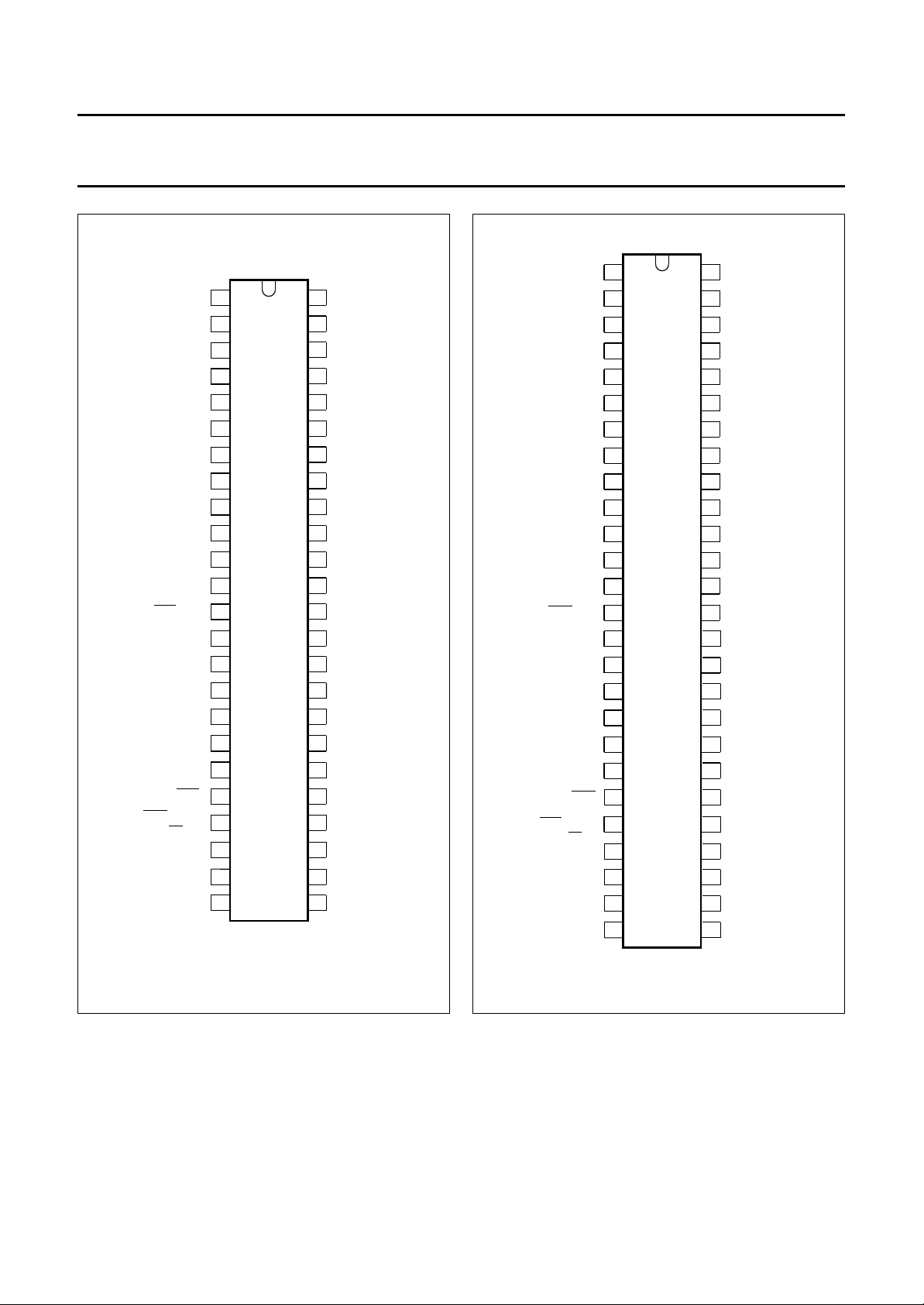
Fig.2 Pin configuration; SOT240-1 (DIP48).
1996 Nov 04 6
Fig.3 Pin configuration; SOT247-1 (SDIP52).
Philips Semiconductors Preliminary specification
Integrated Video input processor and
Teletext decoder (IVT1.8*)
handbook, full pagewidth
i.c.
n.c.
i.c.
i.c.
64
63
62
1
i.c.
i.c.
2
i.c.
3
LINE 23
OSCOUT
OSCGND
4
i.c.
5
i.c.
6
7
i.c.
i.c.
8
n.c.
9
10
n.c.
V
11
DD1
n.c.
12
13
OSCIN
14
15
V
16
SS1
17
n.c.
18
REF+
19
BLACK B
n.c.
61
60
CLK O/P
n.c.
59
58
SAA5281
n.c.
57
i.c.
CLK EN
56
55
n.c.
54
i.c.
53
i.c.
52
51
i.c.
50
i.c.
i.c.
49
i.c.
48
47
i.c.
46
i.c.
i.c.
45
V
44
n.c.
43
42
n.c.
41
n.c.
40
SDA
SCL
39
38
Y
ODD/EVEN
37
(or DV)
36
COR
BLAN
35
34
RGBREF
33
SAA5281
SS3
20
21
22
23
24
25
CVBS
IREF
DD2
V
POL
n.c.
STTV/LFB
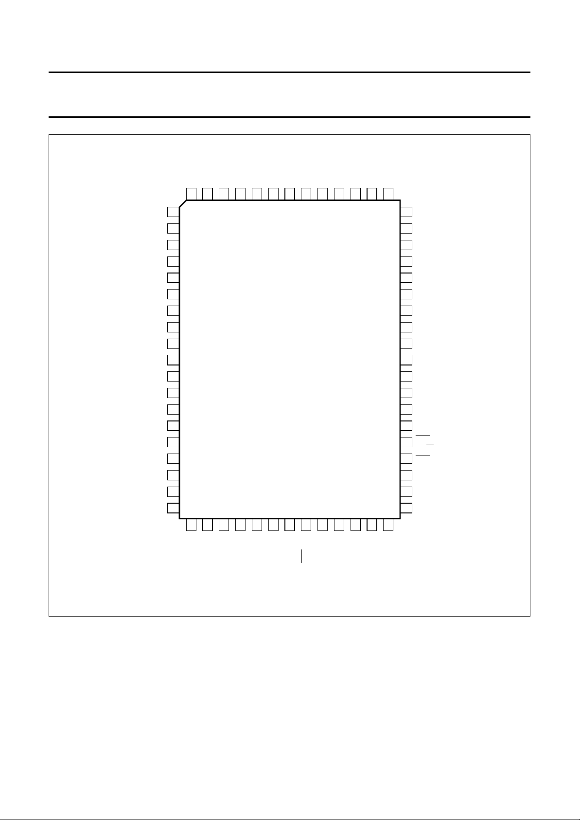
Fig.4 Pin configuration; SOT319-2 (QFP64).
1996 Nov 04 7
26
n.c.
27
28
SS2
V
VCR/FFB
29
n.c.
30
31
32
n.c.
G
MBH665
R
Philips Semiconductors Preliminary specification
Integrated Video input processor and
Teletext decoder (IVT1.8*)
QUALITY AND RELIABILITY
This device will meet Philips Semiconductors General Quality Specification for Business group
Circuits SNW-FQ-611-Part E”
Group A
Table 1 Acceptance tests per lot
TEST REQUIREMENTS
Mechanical cumulative target: <100 ppm
Electrical cumulative target: <100 ppm
Group B
Table 2 Processability tests (by package family)
TEST REQUIREMENTS
Solderability <7% LTPD
Mechanical <15% LTPD
Solder heat resistance <15% LTPD
. The principal requirements are shown in Tables 1 to 4.
(1)
(1)
SAA5281
“Consumer Integrated
Group C
Table 3 Reliability tests (by process family)
TEST CONDITIONS REQUIREMENTS
Operational life 168 hours at Tj= 150 °C <1500 FPM; equivalent to
<100 FITS at Tj=70°C
Humidity life temperature, humidity, bias
<2000 FPM
1000 hours, 85 °C, 85% RH
(or equivalent test)
Temperature cycling performance T
stg(min)
to T
stg(max)
<2000 FPM
Table 4 Reliability tests (by device type)
TEST CONDITIONS REQUIREMENTS
ESD and latch-up ESD Human body model
<15% LTPD
2000 V, 100 pF, 1.5 kΩ
ESD Machine model
<15% LTPD
200 V, 200 pF, 0 Ω
latch-up 100 mA, 1.5 × V
DD
<15% LTPD
(absolute maximum)
Notes to Tables 1 to 4
1. ppm = fraction of defective devices, in parts per million.
LTPD = Lot Tolerance Percent Defective.
FPM = fraction of devices failing at test condition, in Failures Per Million.
FITS = Failures In Time Standard.
(1)
(1)
1996 Nov 04 8
Philips Semiconductors Preliminary specification
Integrated Video input processor and
SAA5281
Teletext decoder (IVT1.8*)
LIMITING VALUES
In accordance with Absolute Maximum Rating System (IEC 134).
SYMBOL PARAMETER MIN. MAX. UNIT
V
DD
V
I
V
O
I
O
I
IOK
T
amb
CHARACTERISTICS
= 5 V ±10%; T
V
DD
SYMBOL PARAMETER CONDITIONS MIN. TYP. MAX. UNIT
Supplies
V
DD
I
DDtot
Inputs
supply voltage (all supplies) −0.3 +6.5 V
input voltage (any input) −0.3 VDD+ 0.5 V
output voltage (any output) −0.3 VDD+ 0.5 V
output current (each output) −±10 mA
DC input or output diode current −±20 mA
operating ambient temperature −20 +70 °C
= −20 to +70 °C; pin numbers refer DIP48 package; unless otherwise specified.
amb
supply voltage 4.5 5.0 5.5 V
total supply current − 75 150 mA
CVBS
V
sync
V
burst(p-p)
sync voltage amplitude 0.1 0.3 0.6 V
colour burst amplitude
0.0 0.3 4.0 V
(peak-to-peak value)
t
d(sync)
delay from CVBS to TCS
−150 0 +150 ns
output from STTV buffer
(nominal video, average of
leading/trailing edge)
∆t
d(sync)
change in sync delay between
0 − 25 ns
all black and all white video
input at nominal levels
V
vid(p-p)
video input voltage amplitude
0.7 1.0 1.4 V
(peak-to-peak value)
V
dat(text)
teletext data voltage amplitude 0.29 0.46 0.71 V
∆f/f display PLL capture range ±7 −−%
Z
source
V
I
source impedance −−250 Ω
input switching voltage level of
1.7 2.0 2.3 V
sync separator
Z
I
C
I
input impedance 2.5 5.0 − kΩ
input capacitance −−10 pF
IREF
R
gnd
V
i
resistor to ground − 27 − kΩ
input voltage − 0.5V
DD
− V
1996 Nov 04 9
Philips Semiconductors Preliminary specification
Integrated Video input processor and
SAA5281
Teletext decoder (IVT1.8*)
SYMBOL PARAMETER CONDITIONS MIN. TYP. MAX. UNIT
POL
V
IL
V
IH
I
LI
C
I
LFB
V
IL
V
IH
I
LI
I
Imax
t
dLFB
VCR/FFB
V
IL
V
IH
I
LI
I
Imax
RGBREF
V
IL
I
LI
SCL
V
IL
V
IH
I
LI
C
I
f
clk
t
r
t
f
Inputs/outputs
LOW level input voltage −0.3 − +0.8 V
HIGH level input voltage 2.0 − VDD+ 0.5 V
input leakage current VI= 0 to V
DD
−10 − +10 µA
input capacitance −−10 pF
LOW level input voltage −0.3 − tbf V
HIGH level input voltage tbf − VDD+ 0.5 V
input leakage current VI= 0 to V
DD
−10 − +10 µA
maximum input current note 1 −1 − +1 mA
delay between LFB front edge
− 250 − ns
and input video line sync
LOW level input voltage −0.3 − +0.8 V
HIGH level input voltage 2.0 − VDD+ 0.5 V
input leakage current VI= 0 to V
DD
−10 − +10 µA
maximum input current note 1 −1 − +1 mA
LOW level input voltage −0.3 − V
input leakage current VI= 0 to V
DD
−10 − +10 µA
DD
V
LOW level input voltage −0.3 − +1.5 V
HIGH level input voltage 3.0 − VDD+ 0.5 V
input leakage current VI= 0 to V
DD
−10 − +10 µA
input capacitance −−10 pF
clock frequency 0 − 100 kHz
input rise time between 10% and 90% −−2µs
input fall time between 90% and 10% −−2µs
C
RYSTAL OSCILLATOR (OSCIN; OSCOUT)
V
osc(p-p)
oscillator voltage amplitude
(peak-to-peak value)
G
v
G
m
C
I
C
fb
small signal voltage gain − 1.0 −
mutual conductance 5.0 −−mS
input capacitance −−10 pF
feedback capacitance − 1 − pF
1996 Nov 04 10
− 1.0 − V
Philips Semiconductors Preliminary specification
Integrated Video input processor and
SAA5281
Teletext decoder (IVT1.8*)
SYMBOL PARAMETER CONDITIONS MIN. TYP. MAX. UNIT
BLACK
C
black
V
black
I
LI
SDA (OPEN-DRAIN INPUT/OUTPUT)
V
IL
V
IH
V
OL
I
LI
C
I
C
L
t
r
t
f
t
f
Outputs
storage capacitor to ground − 100 − nF
black level voltage for nominal
1.8 2.15 2.5 V
sync amplitude
input leakage current VI= 0 to V
DD
−10 − +10 µA
LOW level input voltage −0.3 − +1.5 V
HIGH level input voltage 3.0 − VDD+ 0.5 V
LOW level output voltage IOL= 3 mA 0 − 0.5 V
input leakage current VI= 0 to V
DD
−10 − +10 µA
input capacitance −−10 pF
load capacitance −−400 pF
input rise time between 10% and 90% −−2µs
input fall time between 90% and 10% −−2µs
output fall time between 3 V and 1 V −−200 ns
STTV
G
sttv
gain of STTV relative to video
0.9 1.0 1.1
input
V
∆V
tcs
tcs
TCS voltage amplitude 0.2 0.3 0.45 V
DC shift between TCS output
−−0.15 V
and nominal video output
I
O
C
L
output drive current −−3.0 mA
load capacitance −−100 pF
R, G AND B
V
OL
V
OH
LOW level output voltage IOL= 2 mA 0 − 0.2 V
HIGH level output voltage IOH= −1.6 mA;
V
RGBREF
< VDD− 2V;
V
RGBREF
− 0.25
V
RGBREFVRGBREF
+ 0.5
note 2
| output impedance −−200 Ω
|Z
o
C
L
t
r
t
f
load capacitance −−50 pF
output rise time between 10% and 90% −−20 ns
output fall time between 90% and 10% −−20 ns
BLAN
V
OL
V
OH
C
L
t
r
t
f
LOW level output voltage IOL= 1.6 mA 0 − 0.4 V
HIGH level output voltage IOH= − 0.2 mA 1.1 −−V
I
=0mA −−2.8 V
OH
load capacitance −−50 pF
output rise time between 10% and 90% −−20 ns
output fall time between 90% and 10% −−20 ns
V
1996 Nov 04 11
Philips Semiconductors Preliminary specification
Integrated Video input processor and
SAA5281
Teletext decoder (IVT1.8*)
SYMBOL PARAMETER CONDITIONS MIN. TYP. MAX. UNIT
ODD/EVEN OR DV
V
OL
V
OH
C
L
t
r
t
f
COR AND Y(OPEN-DRAIN OUTPUTS)
V
OH
V
OL
C
L
t
f
I
LO
t
skew
2
C-bus timing (see Fig.5)
I
t
LOW
t
HIGH
t
SU;DAT
t
HD;DAT
t
SU;STO
t
BUF
t
HD;STA
t
SU;STA
LOW level output voltage IOL= 1.6 mA 0 − 0.4 V
HIGH level output voltage IOH= −1.6 mA VDD− 0.4 − V
DD
V
load capacitance −−120 pF
output rise time between 0.6 V and
−−50 ns
2.2 V
output fall time between 0.6 V and
−−50 ns
2.2 V
HIGH level pull-up output
−−VDDV
voltage
LOW level output voltage IOL= 2 mA 0 − 0.4 V
= 5 mA 0 − 1.0 V
I
OL
load capacitance −−25 pF
output fall time load resistor of 1.2 kΩ
−−50 ns
to VDD; measured
between VDD− 0.5 V
and 1.5 V
output leakage current VI= 0 to V
skew delay between display
DD
−10 − +10 µA
−−20 ns
outputs R, G, B, COR, Y and
BLAN
SCL clock LOW time 4.0 −−µs
SCL clock HIGH time 4.0 −−µs
data set-up time 250 −−ns
data hold time 170 −−ns
set-up time from clock HIGH
4.0 −−µs
to STOP
ST ART set-up time following a
4.0 −−µs
STOP
START hold time 4.0 −−µs
ST ART set-up time following a
4.0 −−µs
clock LOW-to-HIGH transition
Notes
1. This current is the maximum allowed into the inputs when line and field flyback signals are connected to these inputs.
Series current limiting resistors must be used to limit the input currents to ±1 mA.
2. Voltage level VOH for R, G and B outputs is taken to be the mean value during the output HIGH time. If higher R, G
and B voltage VOH levels are required RGBREF voltage level may be raised and a pull-up resistor used at each of
these pins provided current specification (IOL) is not exceeded.
1996 Nov 04 12
Philips Semiconductors Preliminary specification
Integrated Video input processor and
Teletext decoder (IVT1.8*)
handbook, full pagewidth
SDA
t
LOW
SCL
SDA
MBC764
t
BUF
t
HD;STA
t
r
t
SU;STA
t
HD;DAT
t
HIGH
SAA5281
t
f
t
SU;DAT
t
SU;STO
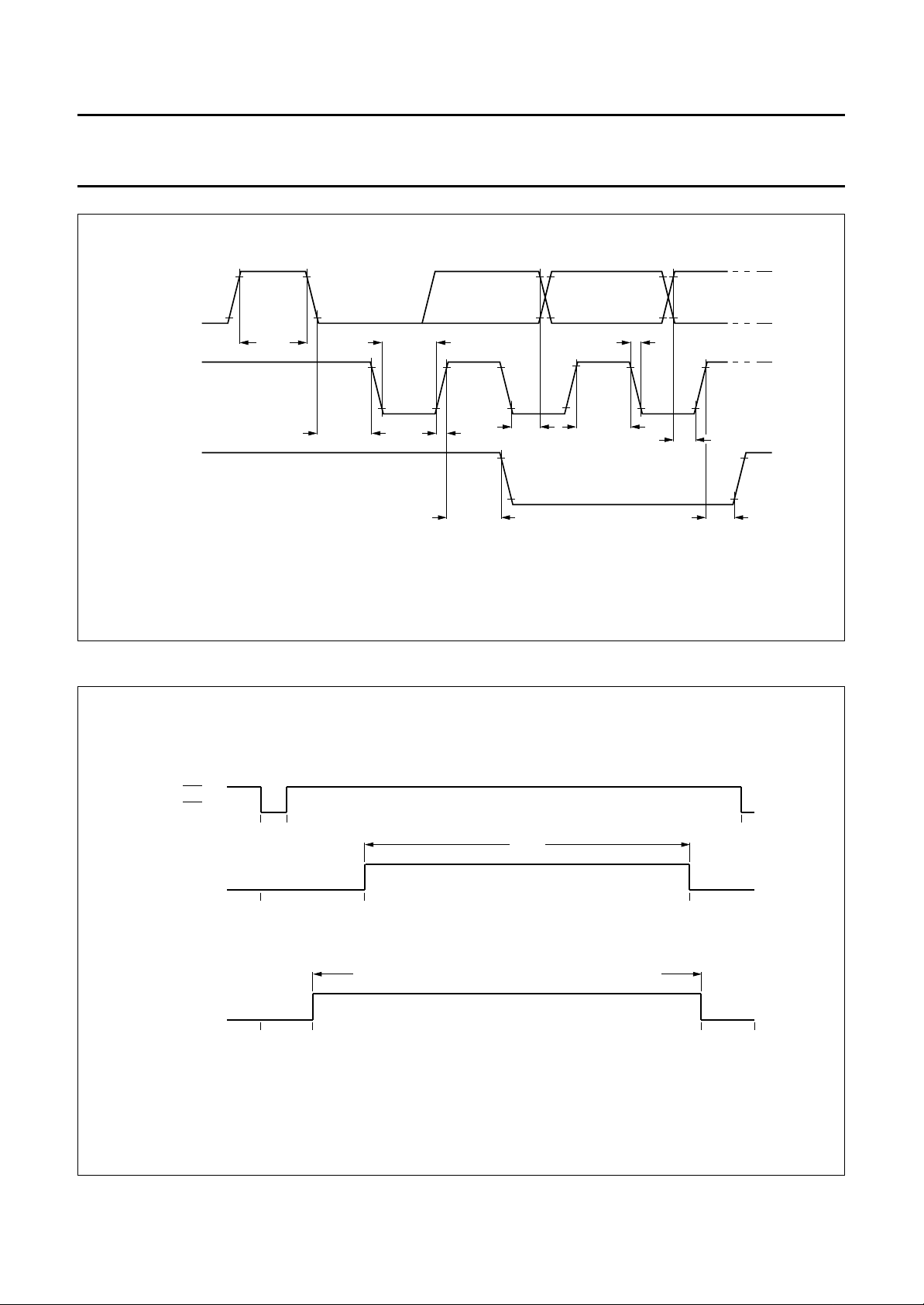
TIMING CHAIN
handbook, full pagewidth
LSP
(TCS)
R, G, B, Y
(1)
R, G, B, Y
(1)
0 4.66
0
0
Fig.5 I2C-bus timing.
40 µs
display period
16.67
lines 42 to 291 inclusive (and 355 to 604 inclusive interlaced)
display period
41
56.67 µs
64 µs
291
line numbers
MLA662 - 1
312
(1) Also BLAN in character and box blanking.
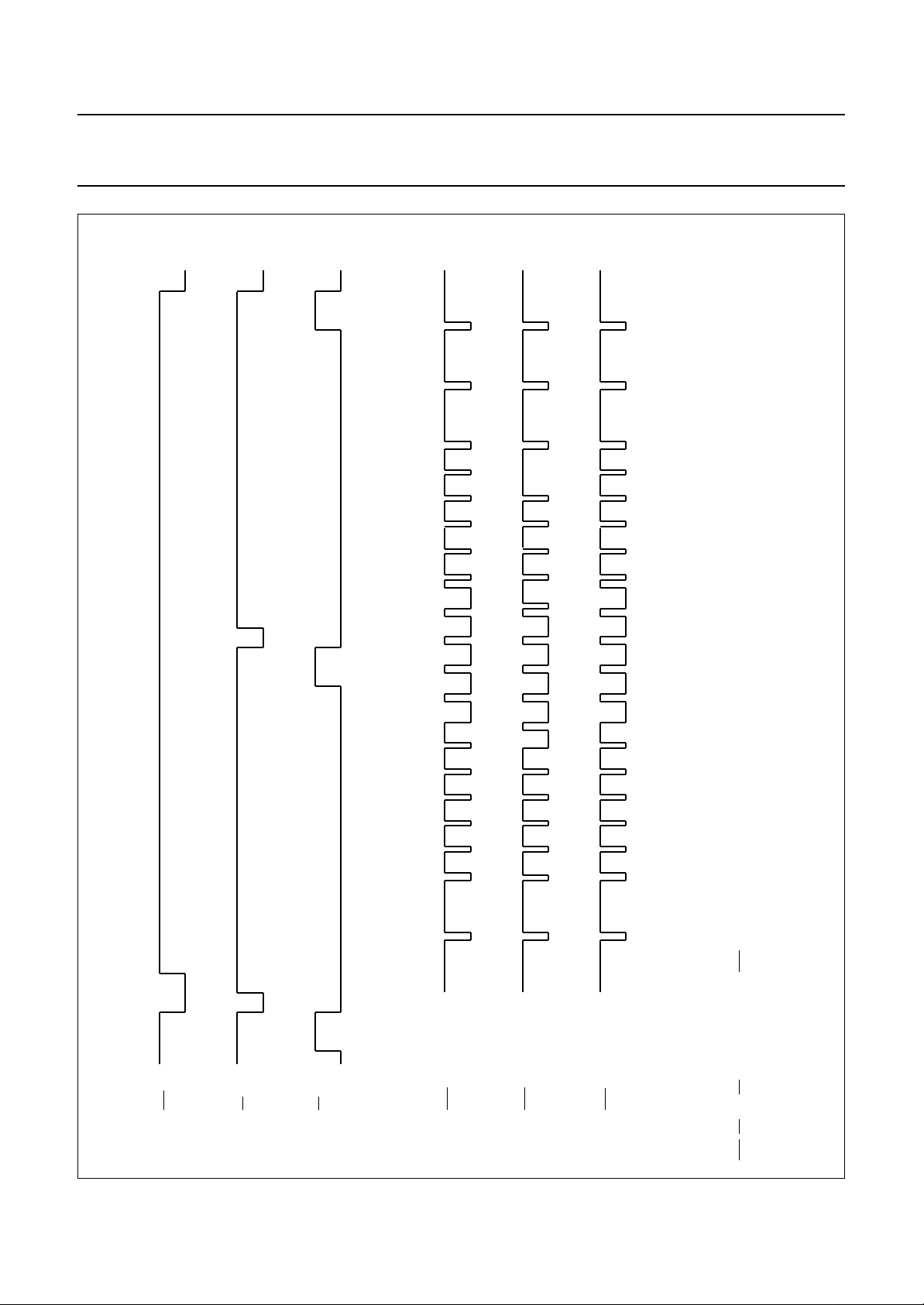
Fig.6 Display output timing (a) line rate (b) field rate.
1996 Nov 04 13
Philips Semiconductors Preliminary specification
Integrated Video input processor and
Teletext decoder (IVT1.8*)
64 µs
64 µs
64 µs
59.33
SAA5281
MLA037 - 2
0 4.66
32 34.33
0 2.33
handbook, full pagewidth
27.33 32
0
1 2 3456 7
625
(312)
624
(311)
623
(310)
622
(309)
621
(308)
309 310 311 312 313 314 (1) 315 (2) 316 (3) 317 (4) 318 (5) 319 (6) 320 (7)
Fig.7 Composite sync waveforms.
308 309 310 311 312 1 2 3 4 5 6 7
LSP
(Line Sync Pulse)
EP
(Equalizing Pulse)
BP
(Broad Pulse)
1996 Nov 04 14
TCS interlaced
TCS interlaced
TCS non-interlaced
LSP, EP and BP are combined to give TCS as shown. All timings are measured from falling edge of LSP.
Line numbers placed in the middle of the line.
Equivalent count numbers in brackets.
Philips Semiconductors Preliminary specification
Integrated Video input processor and
Teletext decoder (IVT1.8*)
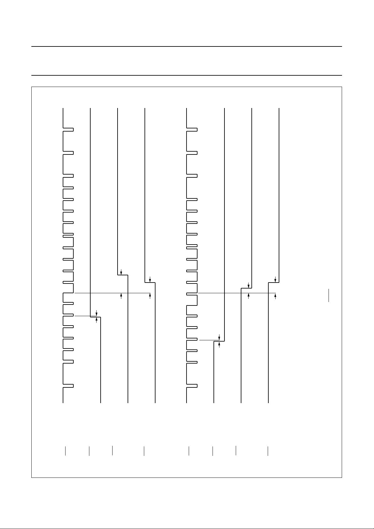
7
SAA5281
MLA416 - 2
320 (7)
FIRST FIELD START (EVEN)
625
(312) 1 2 3 4 5 6
(311)(310)(308) (309)
621 622 623 624
TCS interlaced
2 µs
ODD / EVEN output
(normal sync mode)
48 µs
(1)
30 µs
ODD / EVEN output
(normal sync mode
when VCS to SCS
mode active)
ODD / EVEN output
SECOND FIELD START (ODD)
314 (1) 315 (2) 316 (3) 317 (4) 318 (5) 319 (6)
311
309 310 312 313
(slave sync mode)
TCS interlaced
16 µs
2 µs
ODD / EVEN output
(normal sync mode
ODD / EVEN output
(normal sync mode)
when VCS to SCS
(1)
mode active)
ODD / EVEN output
30 µs
(slave sync mode)
handbook, full pagewidth
Fig.8 ODD/EVEN timing.
1996 Nov 04 15
Line numbers placed in the middle of the line.
Equivalent count numbers in brackets.
(1) Or 62 µs if Register 1 D2.D1.D0 equals 1 1 1.
 Loading...