

Philips SAA5264PS-M3 Datasheet
INTEGRATED CIRCUITS
DATA SH EET
SAA5264; SAA5265
10 and 1 page intelligent teletext
decoders
Preliminary specification
File under Integrated Circuits, IC02
1999 Oct 05

Philips Semiconductors Preliminary specification
10 and 1 page intelligent teletext decoders SAA5264; SAA5265
FEATURES
The following features apply to both SAA5264 and
SAA5265:
• Complete 625 line teletext decoderin one chip reduces
printed circuit board area and cost
• Automatic detection of transmitted fastext links or
service information (packet 8/30)
• On-Screen Display (OSD) for user interface menus
using teletext and dedicated menu icons
• Video Programming System (VPS) decoding
• Wide Screen Signalling (WSS) decoding
• Pan-European, Cyrillic, Greek/Turkish and
French/Arabic character sets in each chip
• High-level command interface via I2C-bus gives easy
control with a low software overhead
• High-level command interface is backward compatible
to Stand-Alone Fastext And Remote Interface (SAFARI)
• 625 and 525 line display
• RGB interface to standard colour decoder ICs, current
source
• Versatile 8-bit open-drain Input/Output (I/O) expander,
5 V tolerant
• Single 12 MHz crystal oscillator
• 3.3 V supply voltage.
SAA5264 features
• Automatic detection of transmitted pages to be selected
by page up and page down
• 8 Page fastext decoder
• Table Of Pages (TOP) decoder with Basic Top Table
(BTT) and Additional Information Tables (AITs)
• 4 Page user-defined list mode.
GENERAL DESCRIPTION
The SAA5264 is a single-chip ten page 625-line World
System Teletext decoder with a high-level command
interface, and is SAFARI compatible.
The SAA5265 is a single-chip one page version of the
SAA5264.
Both devices are designed to minimize the overall system
cost, due to the high-level command interface offering the
benefit of a low software overhead in the TV
microcontroller.
The SAA5264 has the following functionality:
• 10 page teletext decoder with OSD, Fastext, TOP,
default and list acquisition modes
• Automatic channel installation support
• Closed caption acquisition and display
• Violence Chip (VChip) support.
The SAA5265 has the following functionality:
• 1 Page teletext decoder with OSD, fastext and default
acquisition modes
• Automatic channel installation support
• Closed caption acquisition and display
• VChip support
• No EEPROM fitted (there is no list mode feature).
1999 Oct 05 2

Philips Semiconductors Preliminary specification
10 and 1 page intelligent teletext decoders SAA5264; SAA5265
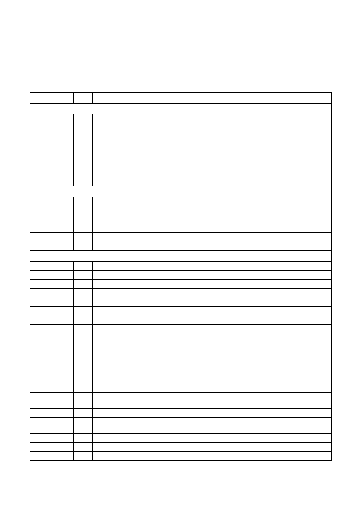
ORDERING INFORMATION
TYPE NUMBER
(1)
PACKAGE
NAME DESCRIPTION VERSION
SAA5264PS/M3/nnnn SDIP52 plastic shrink dual-in-line package; 52 leads (600 mil) SOT247-1
SAA5265PS/M4/nnnn SDIP52 plastic shrink dual-in-line package; 52 leads (600 mil) SOT247-1
Note
1. ‘nnnn’ is a unique four digit number denoting the software version.
QUICK REFERENCE DATA
SYMBOL PARAMETER CONDITIONS MIN. TYP. MAX. UNIT
V
I
DDP
I
DDC
DDX
all supply voltages referenced to V
SS
periphery supply current note 1 1 −−mA
core supply current normal mode − 15 18 mA
3.0 3.3 3.6 V
idle mode − 4.6 6 mA
I
DDA
analog supply current normal mode − 45 48 mA
idle mode − 0.87 1 mA
f
xtal(nom)
T
amb
T
stg
nominal crystal frequency fundamental mode − 12 − MHz
ambient temperature −20 − +70 °C
storage temperature −55 − +125 °C
Note
1. Periphery supply current is dependent on external components and I/O voltage levels.
1999 Oct 05 3
Philips Semiconductors Preliminary specification
10 and 1 page intelligent teletext decoders SAA5264; SAA5265
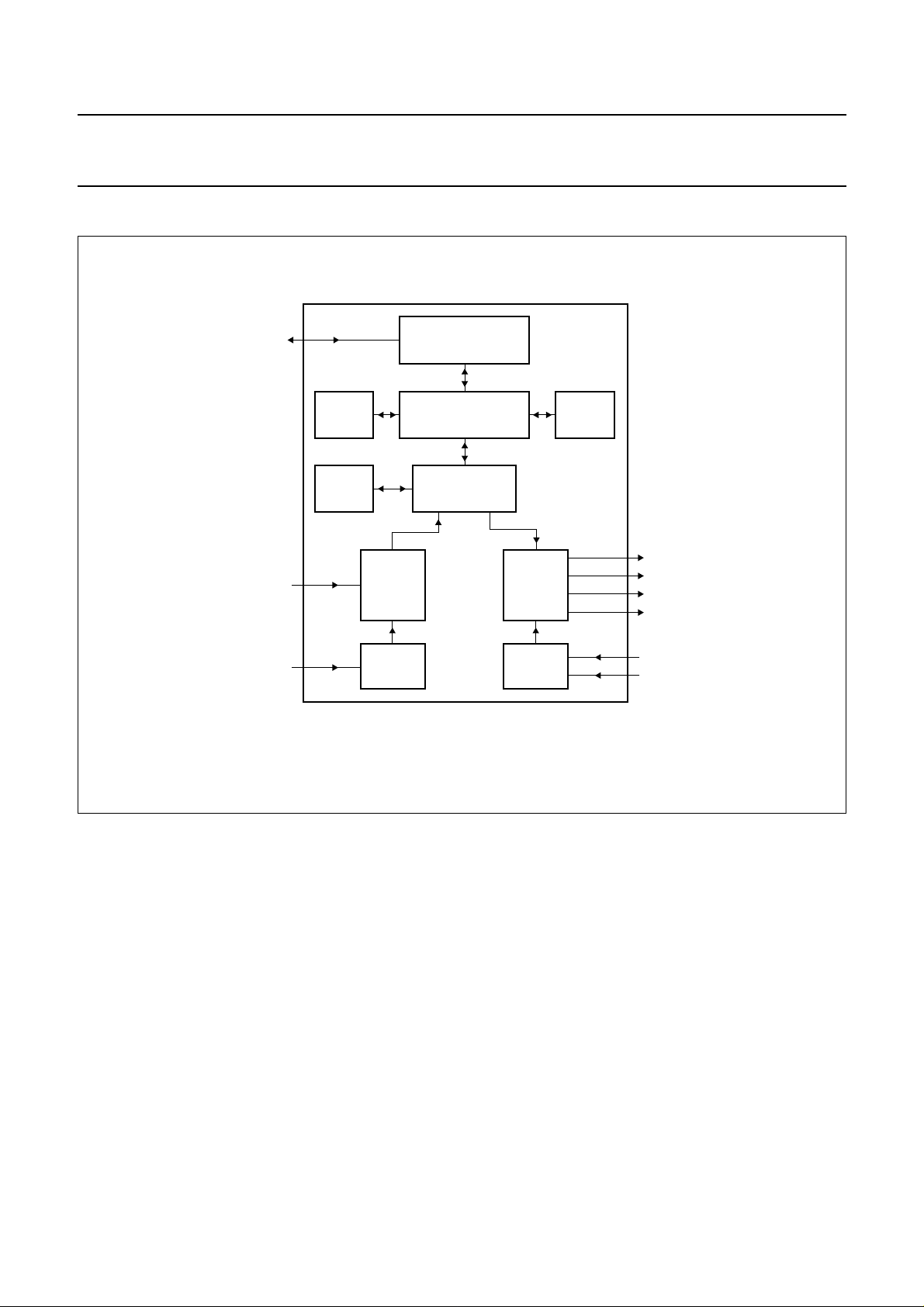
BLOCK DIAGRAM
handbook, full pagewidth
2
I
C-bus,
general I/O
TV CONTROL
AND
INTERFACE
CVBS
CVBS
ROM
DRAM
MICROCONTROLLER
(80C51)
MEMORY
INTERFACE
DATA
CAPTURE
DATA
CAPTURE
TIMING
Fig.1 Block diagram.
SAA5264
SAA5265
DISPLAY
DISPLAY
TIMING
SRAM
R
G
B
VDS
VSYNC
HSYNC
GSA018
1999 Oct 05 4
Philips Semiconductors Preliminary specification
10 and 1 page intelligent teletext decoders SAA5264; SAA5265
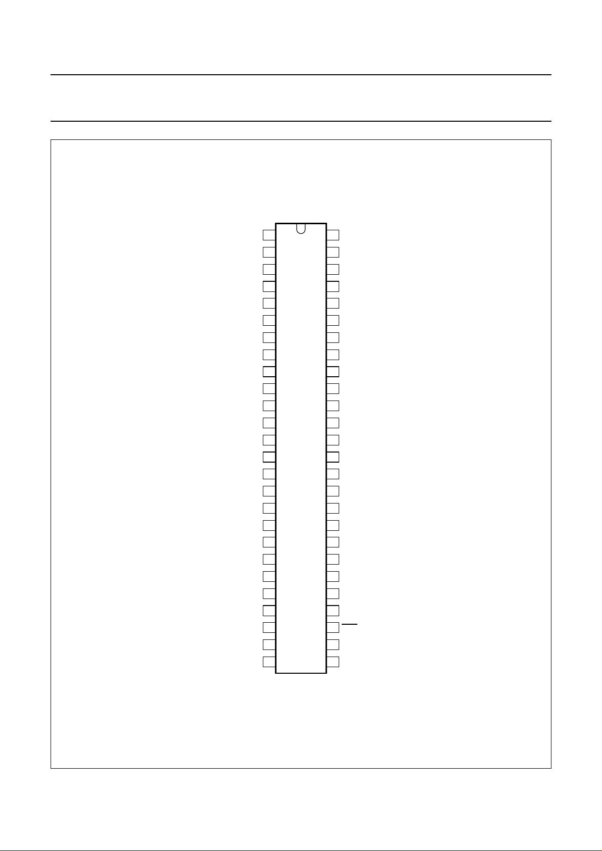
PINNING
SYMBOL PIN TYPE DESCRIPTION
Port 2: 8-bit programmable bidirectional port with alternative functions
P2.0/PWM 1 I/O output for 14-bit high precision Pulse Width Modulator (PWM)
P2.1/PWM0 2 I/O outputs for 6-bit PWMs 0 to 6
P2.2/PWM1 3 I/O
P2.3/PWM2 4 I/O
P2.4/PWM3 5 I/O
P2.5/PWM4 6 I/O
P2.6/PWM5 7 I/O
P2.7/PWM6 8 I/O
Port 3: 8-bit programmable bidirectional port with alternative functions
P3.0/ADC0 9 I/O inputs for the software Analog-to-Digital-Converter (ADC) facility
P3.1/ADC1 10 I/O
P3.2/ADC2 11 I/O
P3.3/ADC3 12 I/O
P3.4/PWM7 30 I/O output for 6-bit PWM7
V
SSC
Port 0: 8-bit programmable bidirectional port
SCL(NVRAM) 14 I I
SDA(NVRAM) 15 I/O I
P0.2 16 I/O input/output for general use
P0.3 17 I/O input/output for general use
P0.4 18 I/O input/output for general use
P0.5 19 I/O 8 mA current sinking capability for direct drive of Light Emitting Diodes (LEDs)
P0.6 20 I/O
P0.7 21 I/O input/output for general use
V
SSA
CVBS0 23 I Composite Video Baseband Signal (CVBS) input; a positive-going 1 V (peak-to-peak)
CVBS1 24 I
SYNC_FILTER 25 I sync-pulse-filter input for CVBS; this pin should be connected to V
IREF 26 I reference current input for analog circuits; for correct operation a 24 kΩ resistor
FRAME 27 O Frame de-interlace output synchronized with the VSYNC pulse to produce a
TEST 28 I not available; connect this pin to V
COR 29 O contrast reduction: open-drain, active LOW output which allows selective contrast
V
DDA
B 32 O Blue colour information pixel rate output
13 − core ground
2
C-bus Serial Clock input to Non-Volatile RAM
2
C-bus Serial Data input/output (Non-Volatile RAM)
22 − analog ground
input is required; connected via a 100 nF capacitor
100 nF capacitor
should be connected to V
SSA
non-interlaced display by adjustment of the vertical deflection circuits
reduction of the TV picture to enhance a mixed mode display
30 I/O P3.4/PWM7 (described above)
31 − analog supply voltage (3.3 V)
SSA
SSA
via a
1999 Oct 05 5
Philips Semiconductors Preliminary specification
10 and 1 page intelligent teletext decoders SAA5264; SAA5265
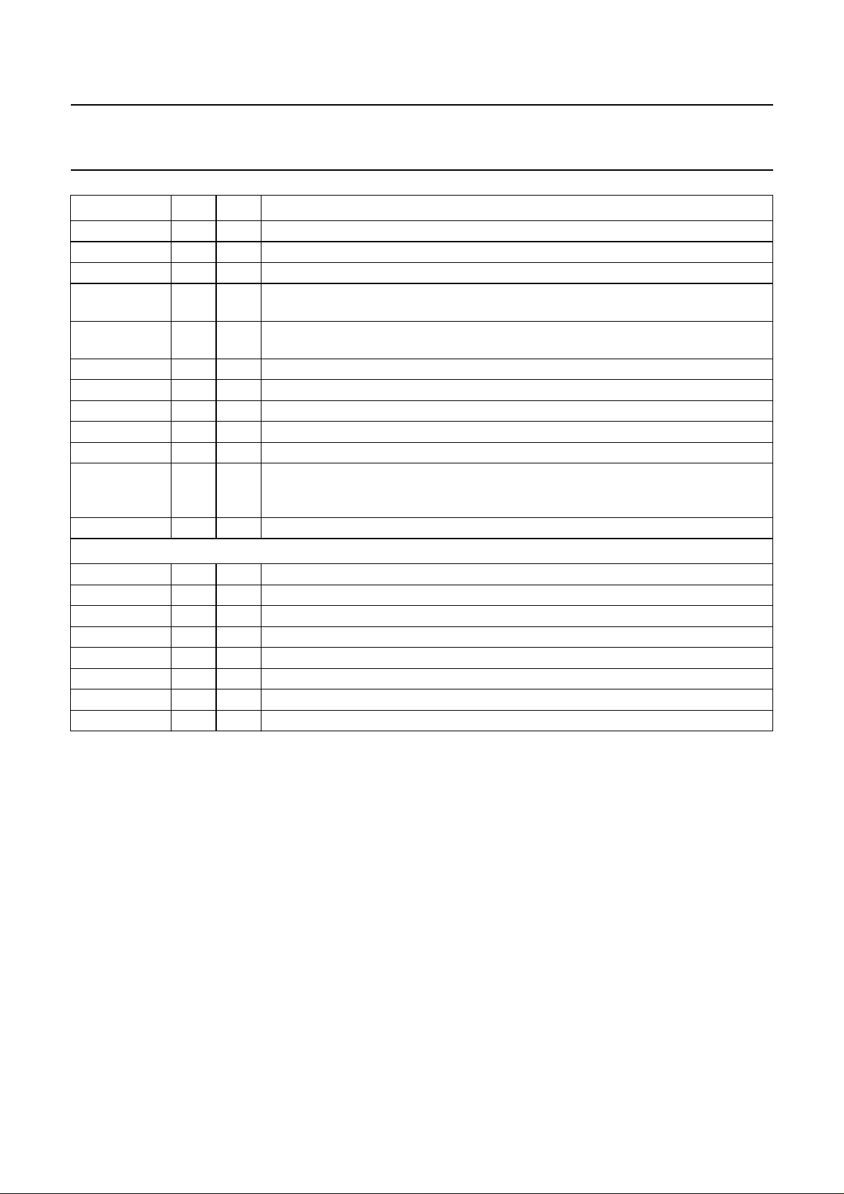
SYMBOL PIN TYPE DESCRIPTION
G 33 O Green colour information pixel rate output
R 34 O Red colour information pixel rate output
VDS 35 O video/data switch push-pull output for pixel rate fast blanking
HSYNC 36 I horizontal sync pulse input: Schmitt triggered for a Transistor Transistor Level (TTL)
version; the polarity of this pulse is programmable by register bit TXT1.HPOLARITY
VSYNC 37 I vertical sync pulse input; Schmitt triggered for a TTL version; the polarity of this pulse
is programmable by register bit TXT1.V POLARITY
V
SSP
V
DDC
OSCGND 40 − crystal oscillator ground
XTALIN 41 I 12 MHz crystal oscillator input
XTALOUT 42 O 12 MHz crystal oscillator output
RESET 43 I reset input; if this pin is HIGH for at least 2 machine cycles (24 oscillator periods)
V
DDP
Port 1: 8-bit programmable bidirectional port
P1.0 45 I/O input/output for general use
P1.1 46 I/O input/output for general use
P1.2 47 I/O input/output for general use
P1.3 48 I/O input/output for general use
SCL 49 I I
SDA 50 I/O I
P1.4 51 I/O input/output for general use
P1.5 52 I/O input/output for general use
38 − periphery ground
39 − core supply voltage (+3.3 V)
while the oscillator is running, the device resets; this pin should be connected to V
via a capacitor
44 − periphery supply voltage (+3.3 V)
2
C-bus Serial Clock input from application
2
C-bus Serial Data input/output (application)
DDP
1999 Oct 05 6
Philips Semiconductors Preliminary specification
10 and 1 page intelligent teletext decoders SAA5264; SAA5265
handbook, halfpage
P2.0/PWM
P2.1/PWM0
P2.2/PWM1
P2.3/PWM2
P2.4/PWM3
P2.5/PWM4
P2.6/PWM5
P2.7/PWM6
P3.0/ADC0
P3.1/ADC1
P3.2/ADC2
P3.3/ADC3
SCL(NVRAM)
SDA(NVRAM)
SYNC_FILTER
V
SSC
P0.2
P0.3
P0.4
P0.5
P0.6
P0.7
V
SSA
CVBS0
CVBS1
IREF
1
2
3
4
5
6
7
8
9
10
11
12
13
14
15
16
17
18
19
20
21
22
23
24
25
26
SAA5264
SAA5265
GSA016
52
P1.5
51
P1.4
50
SDA
49
SCL
48
P1.3
47
P1.2
46
P1.1
45
P1.0
44
V
43
RESET
42
XTALOUT
41
XTALIN
40
OSCGND
39
V
38
V
37
VSYNC
36
HSYNC
35
VDS
34
R
33
G
32
B
31
V
30
P3.4/PWM7
29
COR
28
TEST
27
FRAME
DDP
DDC
SSP
DDA
Fig.2 Pin configuration.
1999 Oct 05 7
Philips Semiconductors Preliminary specification
10 and 1 page intelligent teletext decoders SAA5264; SAA5265
HIGH LEVEL COMMAND INTERFACE
The I2C-bus interface is used to pass control commands and data between the SAA5264/SAA5265 and the television
microcontroller. The interface uses high-level commands, which are backward compatible with the SAFARI.
The I2C-bus transmission formats are:
Table 1 User command
START I2C-BUS ADDRESS WRITE ACK COMMAND ACK STOP
Table 2 System command
2
START I
Table 3 User read
START I
CHARACTER SETS
C-BUS ADDRESS WRITE ACK COMMAND ACK PARAMETER ACK STOP
2
C-BUS ADDRESS READ ACK DATA ACK STOP
The following standard character sets are included in the SAA5264 and in the SAA5265:
Set 0 = Pan-European
Set 1 = Cyrillic
Set 2 = Greek/Turkish
Set 3 = French/Arabic
If you require any other character sets, please discuss them with your local Regional Sales Office first.
LIMITING VALUES
In accordance with Absolute Maximum Rating System (IEC 60134).
SYMBOL PARAMETER CONDITIONS MIN. MAX. UNIT
V
V
DDX
I
all supply voltages −0.5 +4.0 V
input voltage (any input) note 1 −0.5 VDD+0.5
V
or +4.1
V
I
O
I
IO(d)
T
T
O
amb
stg
output voltage (any output) note 1 −0.5 VDD+0.5 V
output current (each output) − 10 mA
diode DC input or output current − 20 mA
ambient temperature −20 +70 °C
storage temperature −55 +125 °C
Note
1. This maximum value refers to 5 V tolerant I/Os and may be 6 V maximum but only when V
is present.
DD
1999 Oct 05 8
 Loading...