

Philips saa5254 DATASHEETS

INTEGRATED CIRCUITS
DATA SH EET
SAA5254
Integrated VIP and teletext decoder
(IVT1.1X)
Preliminary specification
Supersedes data of July 1993
File under Integrated Circuits, IC02
1996 Nov 07
Philips Semiconductors Preliminary specification
Integrated VIP and teletext decoder
(IVT1.1X)
FEATURES
• Complete teletext decoder including page memory and
FASTEXT links in a 40-pin DIP package
• Automatic processing of extension packet 26 for widest
possible language decoding. All our standard language
options can be available, and language option is
readable via I2C-bus
• 100% hardware compatible with the SAA5244A; plug-in
replacement and extra market
• 100% hardware compatible with the SAA5244A, except
if the special OSD symbols were used with the
SAA5244A, except ROM identification number
• The device is pin-aligned with the other members of the
new Philips teletext decoder family, i.e. SAA5280 and
the SAA5249, making one hardware solution for the full
range
• Low software overhead for the control microprocessor
• Single page acquisition system
• RGB interface to standard colour decoder ICs, push-pull
output drive
• Separate text and video signal quality detectors.
SAA5254
DESCRIPTION
The Integrated VIP and Teletext decoder (IVT1.1X) is
designed to decode 625-line based World System Teletext
transmissions. This single-chip teletext decoder hardware
is based on the SAA5244A with which it is completely
compatible.
Like the SAA5244A the device contains all the hardware
necessary to decode the teletext, but the SAA5254 also
contains extra hardware to process the extension packet
26 characters automatically, extending the markets to
which the TV chassis can be shipped and opening the
possibility of many more language options.
ORDERING INFORMATION
TYPE
NUMBER
SAA5254P DIP40
QUICK REFERENCE DATA
SYMBOL PARAMETER MIN. TYP. MAX. UNIT
V
DD
I
DD
V
sync
V
video
f
XTAL
T
amb
NAME DESCRIPTION VERSION
plastic dual in-line package; 40 leads (600 mil)
supply voltage 4.5 5.0 5.5 V
supply current − 90 120 mA
sync voltage amplitude 0.1 0.3 0.6 V
video voltage amplitude 0.7 1.0 1.4 V
crystal frequency − 27 − MHz
operating ambient temperature −20 − +70 °C
PACKAGE
SOT129-1
1996 Nov 07 2
Philips Semiconductors Preliminary specification
Integrated VIP and teletext decoder
(IVT1.1X)
BLOCK DIAGRAM
Y BLAN RGBREF RGB
23 19 21 18 15 to 17 22
DISPLAY
DATA
SLICER
AND
CLOCK
REGENERATOR
ODD/EVENCOR
TELETEXT
ACQUISITION
AND
DECODING
HAMMING
CHECKER
AND
PACKET 26
PROCESSING
ENGINE
PAGE
MEMORY
SAA5254
V
SS1
REF
OSCOUT
OSCIN
5
6
2
3
DCVBS
2
I
C-BUS
INTERFACE
ANALOG
TO
DIGITAL
CONVERTER
CRYSTAL
OSCILLATOR
4 7 9 8 11 13 12
OSCGND BLACK IREF CVBS POL STTV/LFB
TIMING
CHAIN
INPUT
CLAMP
AND SYNC
SEPARATOR
SAA5254
DISPLAY
CLOCK
PHASE
LOCKED
LOOP
VCR/FFB
25
24
10
14
20
SDA
SCL
1
V
DD1
V
DD2
V
SS2
V
SS3
MLB207
1996 Nov 07 3
Fig.1 Block diagram; SOT129 (DIP40).
Philips Semiconductors Preliminary specification
Integrated VIP and teletext decoder
SAA5254
(IVT1.1X)
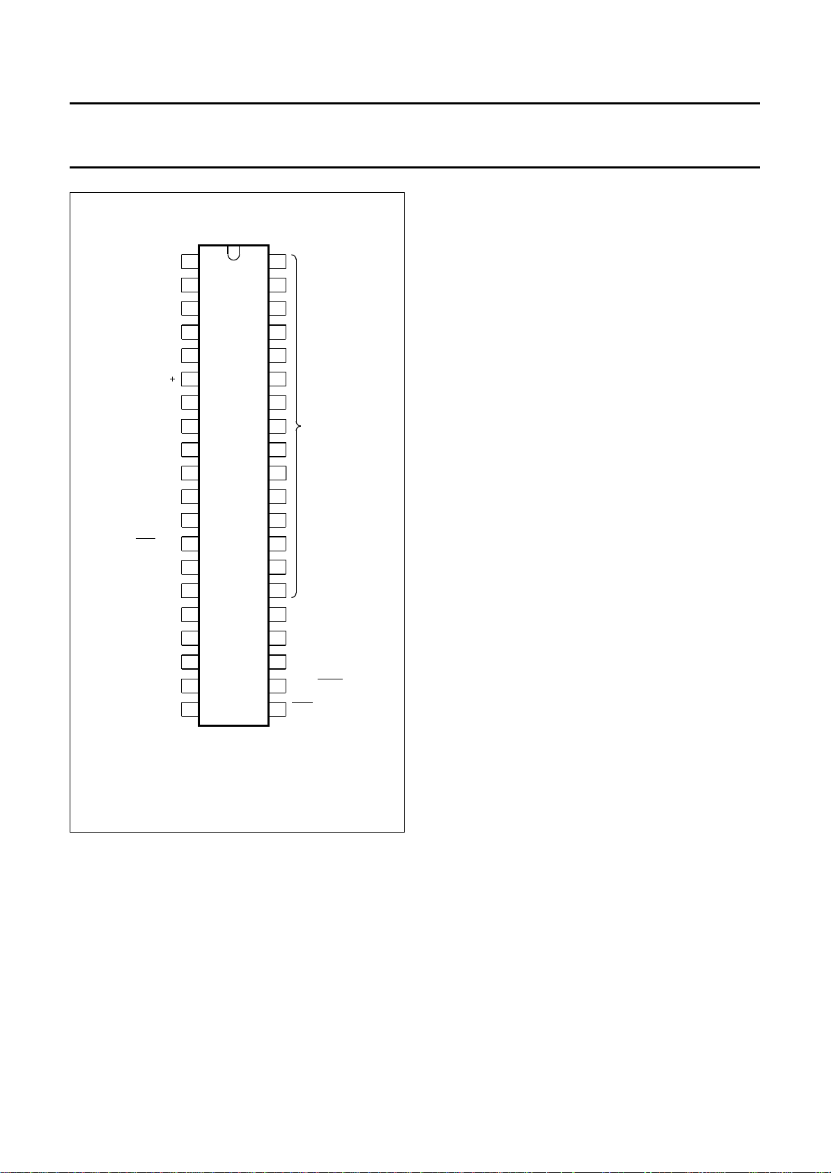
PINNING
SYMBOL PIN DESCRIPTION
V
DD1
OSCOUT 2 27 MHz crystal oscillator output
OSCIN 3 27 MHz crystal oscillator input
OSCGND 4 0 V crystal oscillator ground
V
SS1
REF+ 6 Positive reference voltage for the ADC. This pin should be connected to +5 V.
BLACK 7 Video black level storage pin, connected to ground via a 100 nF capacitor.
CVBS 8 Composite video input pin. A positive-going 1 V (peak-to-peak) input is required,
IREF 9 Reference current input pin, connected to ground via a 27 kΩ resistor.
V
DD2
POL 11 STTV/LFB/FFB polarity selection pin
STTV/LFB 12 Sync to TV output pin/line flyback input pin. Function controlled by an internal register bit
VCR/FFB 13 PLL time constant switch/field flyback input pin. Function controlled by an internal register
V
SS2
R 15 Dot rate character output of the RED colour information.
G 16 Dot rate character output of the GREEN colour information.
B 17 Dot rate character output of the BLUE colour information.
RGBREF 18 DC input voltage to define the output high level on the RGB pins.
BLAN 19 Dot rate fast blanking output.
V
SS3
COR 21 Programmable active LOW output to provide contrast reduction of the TV picture for mixed
EVEN 22 25 Hz output synchronized with the CVBS inputs field sync pulses to produce a
ODD/
Y 23 Dot rate character output of teletext foreground colour information; open drain output.
SCL 24 Serial clock input for the I
SDA 25 Serial input/output data port for the I
i.c. 26 to 40 Internally connected. Must be left open-circuit in application.
1 +5 V supply 1
5 0 V ground 1
connected via a 100 nF capacitor.
10 +5 V supply 2
(scan sync mode).
bit (scan sync mode).
14 0 V ground 2
20 0 V ground 3
text and picture displays or when viewing newsflash/subtitle pages; open drain output.
non-interlaced display by adjustment of the vertical deflection currents.
power-down of the device.
2
C-bus. It can still be driven during power-down of the device.
2
C-bus; open drain output. It can still be driven during
1996 Nov 07 4
Philips Semiconductors Preliminary specification
Integrated VIP and teletext decoder
(IVT1.1X)
V
DD1
OSCOUT
OSCIN
OSCGND
V
SS1
REF
BLACK
CVBS
IREF
V
DD2
POL
STTV/LFB
VCR/FFB
V
SS2
R
G
1
2
3
4
5
6
7
8
9
10
SAA5254
11
12
13
15
16
40
39
38
37
36
35
34
i.c.
33
32
31
30
29
28
2714
26
25
SDA
SAA5254
24
SCL
23
Y
ODD/EVEN
22
COR
21
RGBREF
BLAN
V
SS3
17
B
18
19
20
MLB208
Fig.2 Pin configuration; SOT129 (DIP40).
1996 Nov 07 5
Philips Semiconductors Preliminary specification
Integrated VIP and teletext decoder
SAA5254
(IVT1.1X)
QUALITY AND RELIABILITY
This device will meet Philips Semiconductors General Quality Specification for Business group
Circuits SNW-FQ-611-Part E”
. The principal requirements are shown in Tables 1 to 4.
Group A
Table 1 Acceptance tests per lot
TEST CONDITIONS REQUIREMENTS
Mechanical cumulative target < 100 ppm
Electrical cumulative target < 100 ppm
Group B
Table 2 Processability tests (by package family)
TEST CONDITIONS REQUIREMENTS
Solderability < 7% LTPD
Mechanical < 15% LTPD
Solder heat resistance < 15% LTPD
“Consumer Integrated
(1)
(1)
Group C
Table 3 Reliability tests (by process family)
TEST CONDITIONS REQUIREMENTS
Operational life 168 hours at Tj= 150 °C < 1500 FPM; equivalent to
< 100 FITS at Tj=70°C
Humidity life temperature, humidity, bias
< 2000 FPM
(1000 hours, 85 °C, 85% RH or
equivalent test)
Temperature cycling performance T
stg(min)
to T
stg(max)
< 2000 FPM
Table 4 Reliability tests (by device type)
TEST CONDITIONS REQUIREMENTS
ESD and latch-up ESD Human body model
< 15% LTPD
2000 V, 100 pF, 1.5 kΩ
ESD Machine model
< 15% LTPD
200 V, 100 pF, 1.5 kΩ
latch-up 100 mA, 1.5 × V
DD
< 15% LTPD
(absolute maximum)
Notes to Tables 1 to 4
1. ppm = fraction of defective devices, in parts per million.
LTPD = Lot Tolerance Percent Defective.
FPM = fraction of devices failing at test condition, in Failures Per Million.
FITS = Failures In Time Standard.
(1)
(1)
1996 Nov 07 6
Philips Semiconductors Preliminary specification
Integrated VIP and teletext decoder
SAA5254
(IVT1.1X)
LIMITING VALUES
In accordance with the Absolute Maximum Rating System (IEC 134).
SYMBOL PARAMETER MIN. MAX. UNIT
V
DD
V
I
V
O
I
O
I
IOK
T
amb
CHARACTERISTICS
=5V±10%; T
V
DD
SYMBOL PARAMETER CONDITIONS MIN. TYP. MAX. UNIT
Supply
V
DD
I
DD(tot)
Inputs
supply voltage (all supplies) −0.3 +6.5 V
input voltage (any input) −0.3 VDD+ 0.5 V
output voltage (any output) −0.3 VDD+ 0.5 V
output current (each output) −10 +10 mA
DC input or output diode current −20 +20 mA
operating ambient temperature −20 +70 °C
= −20 to +70 °C, unless otherwise specified.
amb
supply voltage 4.5 5.0 5.5 V
total supply current − 90 120 mA
CVBS
V
sync
t
d(sync)
∆t
d(sync)
V
video(p-p)
PLL
catch
Z
source
C
i
IREF
R
GND
POL
V
IL
V
IH
I
LI
C
i
sync voltage amplitude 0.1 0.3 0.6 V
delay from CVBS to TCS output from
−150 0 +150 ns
STTV buffer (nominal video, average
of leading/trailing edge)
change in sync delay between all
0 − 25 ns
black and all white video input at
nominal levels
video input voltage amplitude
0.7 1.0 1.4 V
(peak-to-peak value)
display PLL catching range ±7 −−%
source impedance −−250 Ω
input capacitance −−10 pF
resistance to ground − 27 − kΩ
LOW level input voltage −0.3 − +0.8 V
HIGH level input voltage 2.0 − VDD+ 0.5 V
input leakage current VI=0toV
DD
−10 − +10 µA
input capacitance −−10 pF
1996 Nov 07 7
Philips Semiconductors Preliminary specification
Integrated VIP and teletext decoder
SAA5254
(IVT1.1X)
SYMBOL PARAMETER CONDITIONS MIN. TYP. MAX. UNIT
LBF
V
IL
V
IH
I
LI
I
I
t
d(LFB)
VCR/FFB
V
IL
V
IH
I
LI
I
I
RGBREF (note 2)
V
I
I
LI
I
DC
SCL
V
IL
V
IH
I
LI
f
SCL
t
i(r)
t
i(f)
C
i
Inputs/outputs
LOW level input voltage −0.3 − +0.8 V
HIGH level input voltage 2.0 − VDD+ 0.5 V
input leakage current VI=0toV
DD
−10 − +10 µA
input current note 1 −1 − +1 mA
delay between LFB front edge and
− 250 − ns
input video line sync
LOW level input voltage −0.3 − +0.8 V
HIGH level input voltage 2.0 − VDD+ 0.5 V
input leakage current VI=0toV
DD
−10 − +10 µA
input current note 1 −1 − +1 mA
input voltage −0.3 − VDD+ 0.5 V
input leakage current VI=0toV
DD
−10 − +10 µA
DC current −−10 mA
LOW level input voltage −0.3 − +1.5 V
HIGH level input voltage 3.0 − VDD+ 0.5 V
input leakage current VI=0toV
DD
−10 − +10 µA
clock frequency 0 − 100 kHz
input rise time 10% to 90% −−2µs
input fall time 90% to 10% −−2µs
input capacitance −−10 pF
C
RYSTAL OSCILLATOR (OSCIN; OSCOUT)
f
XTAL
G
v
G
m
C
i
C
FB
crystal frequency − 27 − MHz
small signal voltage gain 3.5 −−
mutual conductance f = 100 kHz 1.5 −− mA/V
input capacitance −−10 pF
feedback capacitance −−5pF
BLACK
C
I
black
LI
storage capacitor to ground − 100 − nF
input leakage current VI=0toV
1996 Nov 07 8
DD
−10 − +10 µA
Philips Semiconductors Preliminary specification
Integrated VIP and teletext decoder
SAA5254
(IVT1.1X)
SYMBOL PARAMETER CONDITIONS MIN. TYP. MAX. UNIT
SDA
V
IL
V
IH
I
LI
C
i
t
i(r)
t
i(f)
V
OL
t
o(f)
C
L
Outputs
STTV
G
STTV
V
TCS
V
DCshift
I
O
C
L
R, G AND B
V
OL
V
OH
output impedance −−200 Ω
Z
o
C
L
I
DC
t
o(r)
t
o(f)
BLAN
V
OL
V
OH
V
O(max)
C
L
t
o(r)
t
o(f)
LOW level input voltage −0.3 − +1.5 V
HIGH level input voltage 3.0 − VDD+ 0.5 V
input leakage current VI=0toV
DD
−10 − +10 µA
input capacitance −−10 pF
input rise time 10% to 90% −−2µs
input fall time 90% to 10% −−2µs
LOW level output voltage IOL= 3 mA 0 − 0.5 V
output fall time 3 to 1 V −−200 ns
load capacitance −−400 pF
gain of STTV relative to video input 0.9 1.0 1.1
TCS voltage amplitude 0.2 0.3 0.45 V
DC voltage shift between TCS output
−−0.15 V
and nominal video output
output drive current −−3.0 mA
load capacitance −−100 pF
LOW level output voltage IOL= 2 mA 0 − 0.2 V
HIGH level output voltage IOH= −1.6 mA;
RGBREF ≤ VDD− 2V
RGBREF
−0.25 V
RGBREF RGBREF
+0.25 V
V
load capacitance −−50 pF
DC current −−−3.3 mA
output rise time 10% to 90% −−20 ns
output fall time 90% to 10% −−20 ns
LOW level output voltage IOL= 1.6 mA 0 − 0.4 V
HIGH level output voltage IOH= −0.2 mA;
1.1 −− V
VDD= 4.5 V
= 0 mA; VDD= 5.5 V −−2.8 V
I
OH
allowed output voltage at pin with external pull-up −−VDDV
load capacitance −−50 pF
output rise time 10% to 90% −−20 ns
output fall time 90% to 10% −−20 ns
1996 Nov 07 9
Philips Semiconductors Preliminary specification
Integrated VIP and teletext decoder
SAA5254
(IVT1.1X)
SYMBOL PARAMETER CONDITIONS MIN. TYP. MAX. UNIT
ODD/
EVEN
V
OL
V
OH
C
L
t
o(r)
t
o(f)
COR AND Y(OPEN DRAIN)
V
pu
V
OL
C
L
t
o(f)
I
LO
T
skew
LOW level output voltage IOL= 1.6 mA 0 − 0.4 V
HIGH level output voltage IOH= −1.6 mA VDD− 0.4 − V
DD
V
load capacitance −−120 pF
output rise time 0.6 to 2.2 V −−50 ns
output fall time 2.2 to 0.6 V −−50 ns
pull-up voltage at pin −−VDDV
LOW level output voltage IOL= 5 mA 0 − 1.0 V
load capacitance −−25 pF
output fall time load resistor of
−−50 ns
1.2 kΩ to VDD;
measured between
VDD− 0.5 and 1.5 V
output leakage current VI=0toV
skew delay between display outputs
DD
−10 − +10 µA
−−20 ns
R, G, B, COR, Y and BLAN
Timing
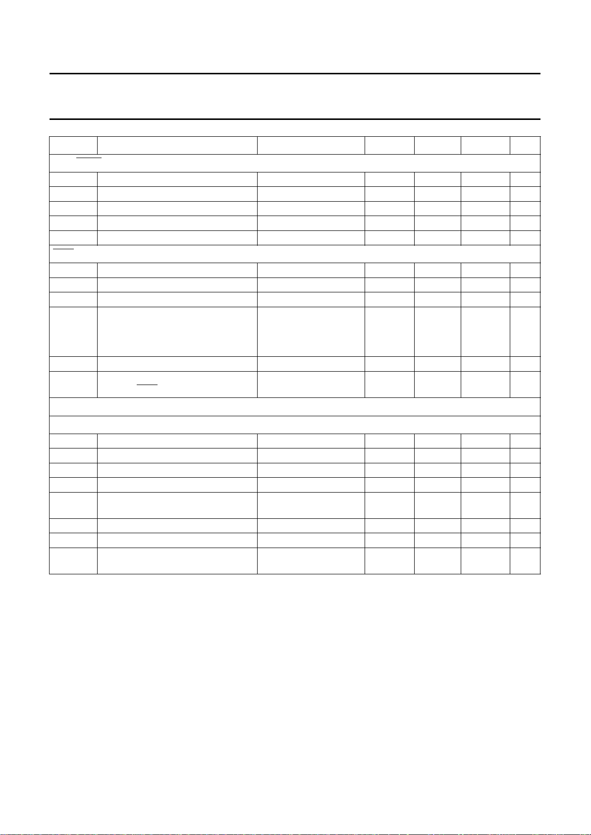
I2C-BUS (see Fig.3)
t
LOW
t
HIGH
t
SU;DAT
t
HD;DAT
t
SU;STO
clock LOW period 4 −− µs
clock HIGH period 4 −− µs
data set-up time 250 −− ns
data hold time 170 −− ns
set-up time from clock HIGH to
4 −− µs
STOP
t
BUF
t
HD;STA
t
SU;STA
START set-up time following a STOP 4 −− µs
START hold time 4 −− µs
START set-up time following clock
4 −− µs
LOW-to-HIGH transition
Notes
1. This current is the maximum allowed into the inputs when line and field flyback signals are connected to these inputs.
Series current limiting resistors must be used to limit the input currents to ±1 mA.
2. RGBREF is the positive supply for the RGB output pins and it must be able to source the IOH current from the
R, G and B pins. The leakage specification on RGBREF only applies when there is no current load on the RGB pins.
1996 Nov 07 10
Philips Semiconductors Preliminary specification
Integrated VIP and teletext decoder
(IVT1.1X)
handbook, full pagewidth
SDA
t
SCL
SDA
MBC764
t
BUF
t
HD;STA
LOW
t
r
t
SU;STA
t
HD;DAT
t
HIGH
SAA5254
t
f
t
SU;DAT
t
SU;STO
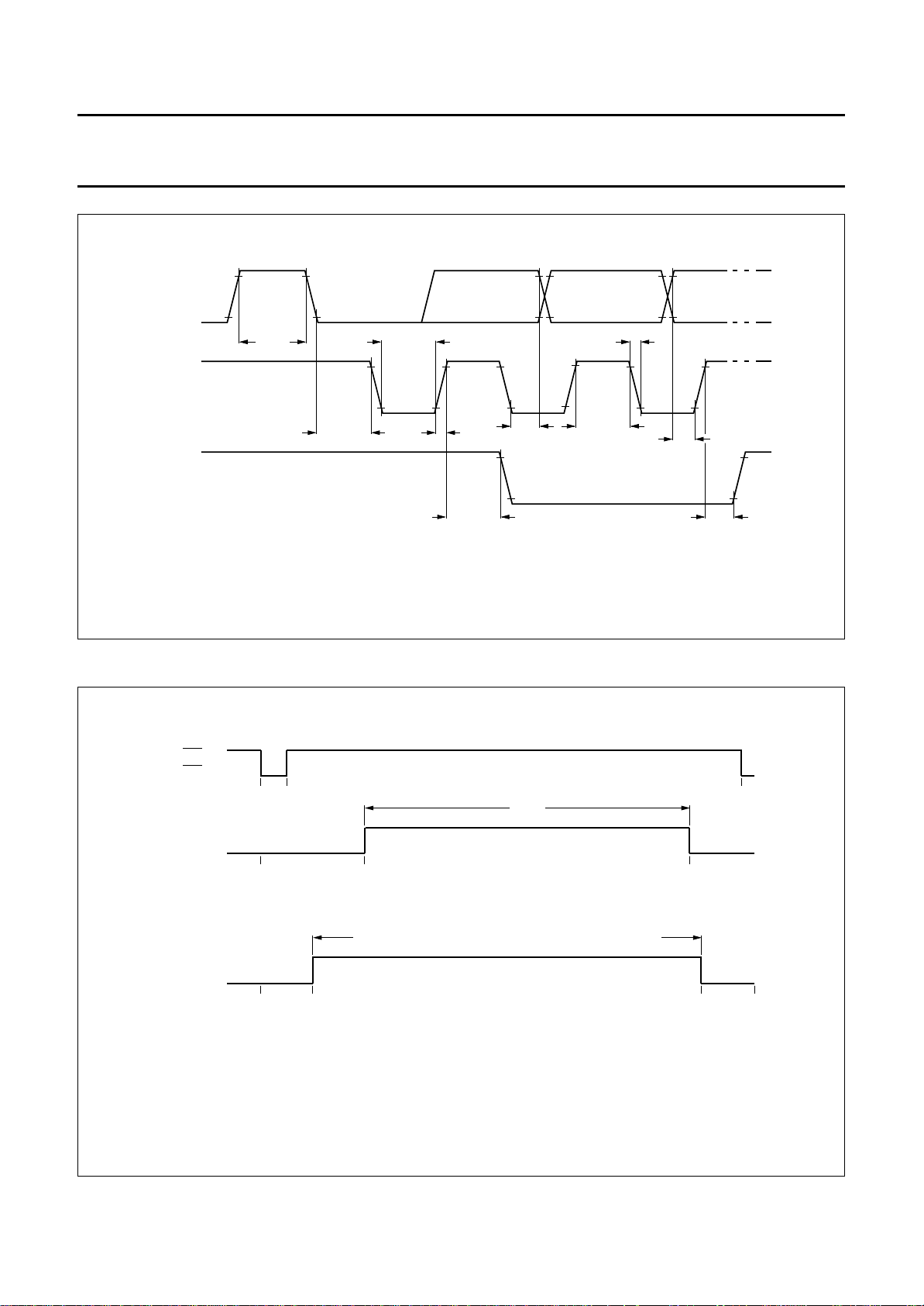
TIMING CHAIN
handbook, full pagewidth
LSP
(TCS)
R, G, B, Y
(1)
R, G, B, Y
(1)
0 4.66
0
0
Fig.3 I2C-bus timing.
40 µs
display period
16.67
(a)
lines 42 to 291 inclusive (and 355 to 604 inclusive interlaced)
display period
41
(b)
56.67 µs
64 µs
291
line numbers
MLA662 - 1
312
(1) Also BLAN in character and box blanking.
1996 Nov 07 11
Fig.4 Display output timing (a) line rate (b) field rate.
 Loading...