

Philips saa5252 DATASHEETS
INTEGRATED CIRCUITS
DATA SH EET
SAA5252
Line twenty-one acquisition and
display (LITOD)
Product specification
Supersedes data of March 1995
File under Integrated Circuits, IC02
1996 Jul 18
Philips Semiconductors Product specification
Line twenty-one acquisition and display (LITOD) SAA5252
FEATURES
• Complete ‘stand-alone’ Line 21 decoder in one package
• On-chip display RAM allowing full page Text mode
• Enhanced character display modes
• Full colour captions
• RGB interface for standard colour decoder ICs
• Automatic handling of Field 2 data
• Automatic selection of (1H, 1V), (2H, 1V) or (2H, 2V)
scan modes
• Onboard OSD facility using Character generator
• RGB inputs to support existing OSD ICs
2
C-bus or ‘stand-alone’ pin control
• I
• Automatic data-ready signal generation on data
acquisition
• Can decode signals recorded on standard VHS and
S-VHS tape.
GENERAL DESCRIPTION
The SAA5252 (LITOD) is a single-chip CMOS device,
which will acquire, decode and display Line 21 Closed
Captioning data from a 525-line composite video signal.
Operation as an On-Screen Display (OSD) device is also
possible. Normal and line progressive scan modes are
supported.
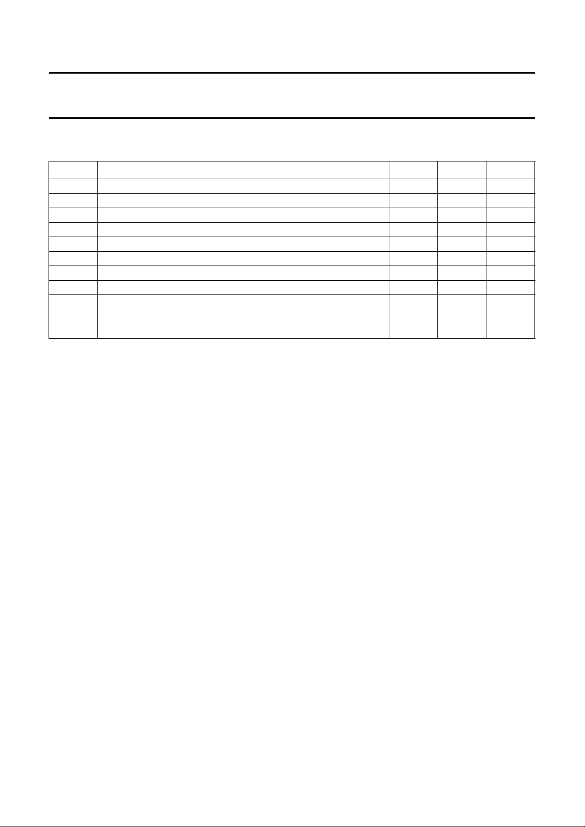
QUICK REFERENCE DATA
SYMBOL PARAMETER MIN. TYP. MAX. UNIT
V
DD
I
DD
V
syn
V
vid
T
amb
T
stg
supply voltage 4.5 5.0 5.5 V
supply current − 30 − mA
CVBS sync amplitude 0.1 0.3 0.6 V
CVBS video amplitude 0.7 1.0 1.4 V
operating ambient temperature −20 − +70 °C
storage temperature −55 − +125 °C
ORDERING INFORMATION
TYPE
NUMBER
NAME DESCRIPTION VERSION
PACKAGE
SAA5252P DIP24 plastic dual in-line package; 24 leads (600 mil) SOT101-1
SAA5252T SO24 plastic small outline package; 24 leads; body width 7.5 mm SOT137-1
1996 Jul 18 2
Philips Semiconductors Product specification
Line twenty-one acquisition and display (LITOD) SAA5252
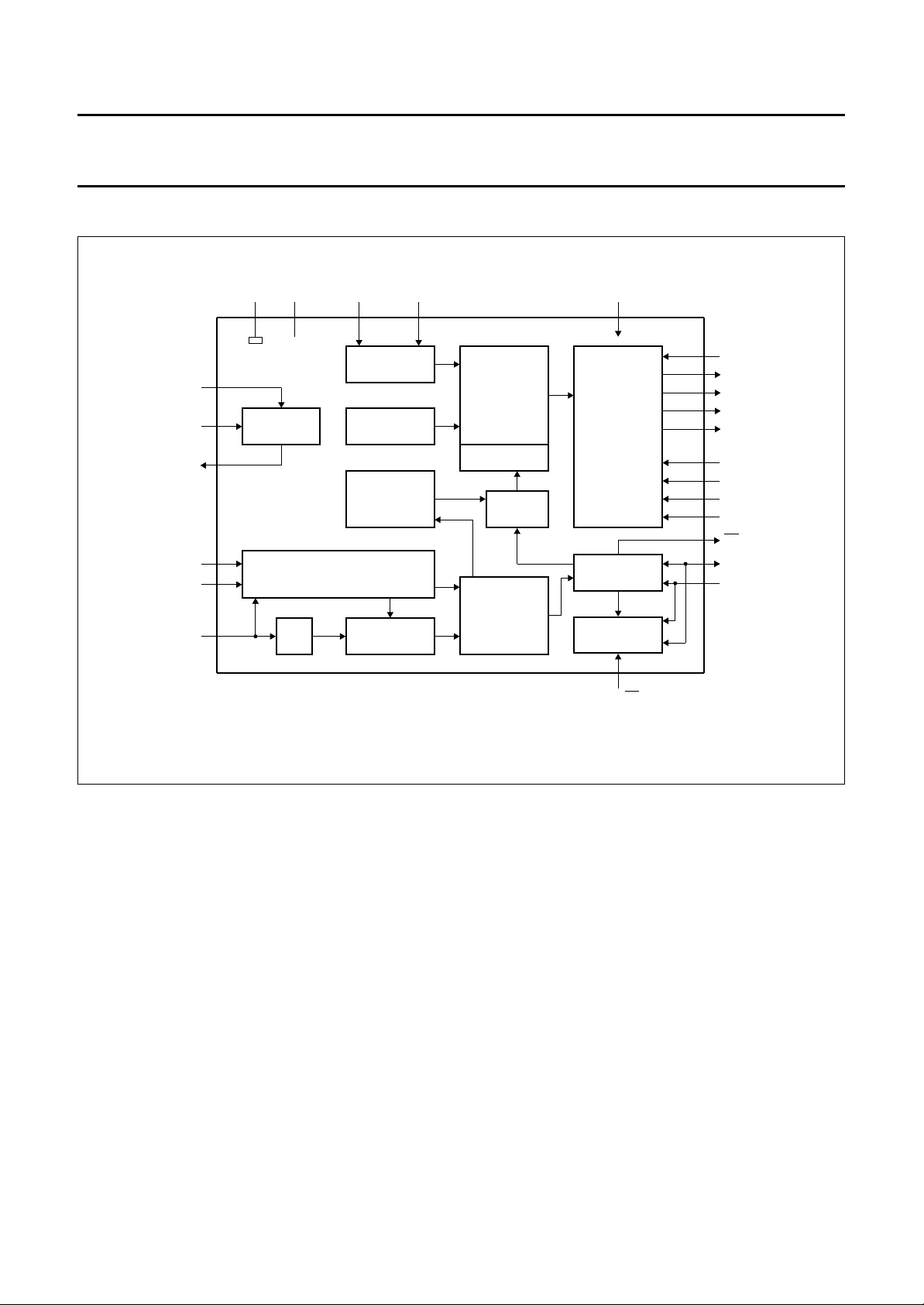
BLOCK DIAGRAM
V
V
SS DD
VH
i.c.
OSCIN
OSCGND
OSCOUT
BLACK
IREF
CVBS
19 18
21
22
OSCILLATOR
20
SAA5252
23
24
1
SYNC SEPARATOR
ACQUISITION TIMING
ADC
7 86
DISPLAY
TIMING
CHARACTER
ROM
CODE
INTERPRETER
AND
ADDRESSING
AND
DATA
DETECTOR
Fig.1 Block diagram.
CHARACTER
GENERATOR
ADDRESSING
PAGE
RAM
SERIAL/
PARALLEL
AND
PARITY
17
RGBREF
16
BLAN
15
R
ROUNDING
ITALICS
AND
RGB
MULTIPLEXOR
2
I C
INTERFACE
CONTROL
2
2
I C/DC
14
13
9
10
11
12
5
3
4
G
B
BLANIN
RIN
GIN
BIN
DR
SDA
SCL
MBB623 - 1
1996 Jul 18 3
Philips Semiconductors Product specification
Line twenty-one acquisition and display (LITOD) SAA5252
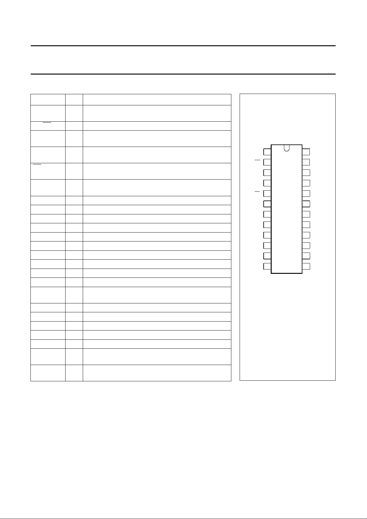
PINNING
SYMBOL PIN DESCRIPTION
CVBS 1 composite video input; signal should be connected via a
100 nF capacitor
2
C/DC 2 input selects I2C or Direct Control
I
2
SDA 3 serial data port for I
direct control
SCL 4 serial clock input for I
direct control
DR 5 data-ready signal to microcontroller (active-LOW) or
mode select input for direct control
i.c. 6 internally connected; connect to V
operation
V 7 vertical reference input for display timing
H 8 horizontal reference input for display timing
BLANIN 9 video blanking input from external OSD device
RIN 10 RED video input from external OSD device
GIN 11 GREEN video input from external OSD device
BIN 12 BLUE video input from external OSD device
B 13 BLUE video output
G 14 GREEN video output
R 15 RED video output
BLAN 16 video blanking output
RGBREF 17 input voltage defining output HIGH level for RGB pins
for closed captioning output
V
DD
V
SS
18 +5 V supply
19 0 V ground
OSCOUT 20 oscillator output
OSCIN 21 oscillator input
OSCGND 22 oscillator ground
BLACK 23 video black level storage input; connected to V
100 nF capacitor
IREF 24 reference current input; connected to V
resistor
C-bus or mode select input for
2
C-bus or mode select input for
for normal
SS
SS
via 27 kΩ
SS
via
1
CVBS
2
I C/DC
BLANIN
SDA
SCL
DR
i.c.
RIN
GIN
BIN
2
3
4
5
6
V
H
SAA5252
7
8
9
10
11
12
MBB622 - 1
Fig.2 Pin configuration.
24
23
22
21
20
19
18
17
16
15
14
13
IREF
BLACK
OSCGND
OSCIN
OSCOUT
V
SS
V
DD
RGBREF
BLAN
R
G
B
1996 Jul 18 4
Philips Semiconductors Product specification
Line twenty-one acquisition and display (LITOD) SAA5252
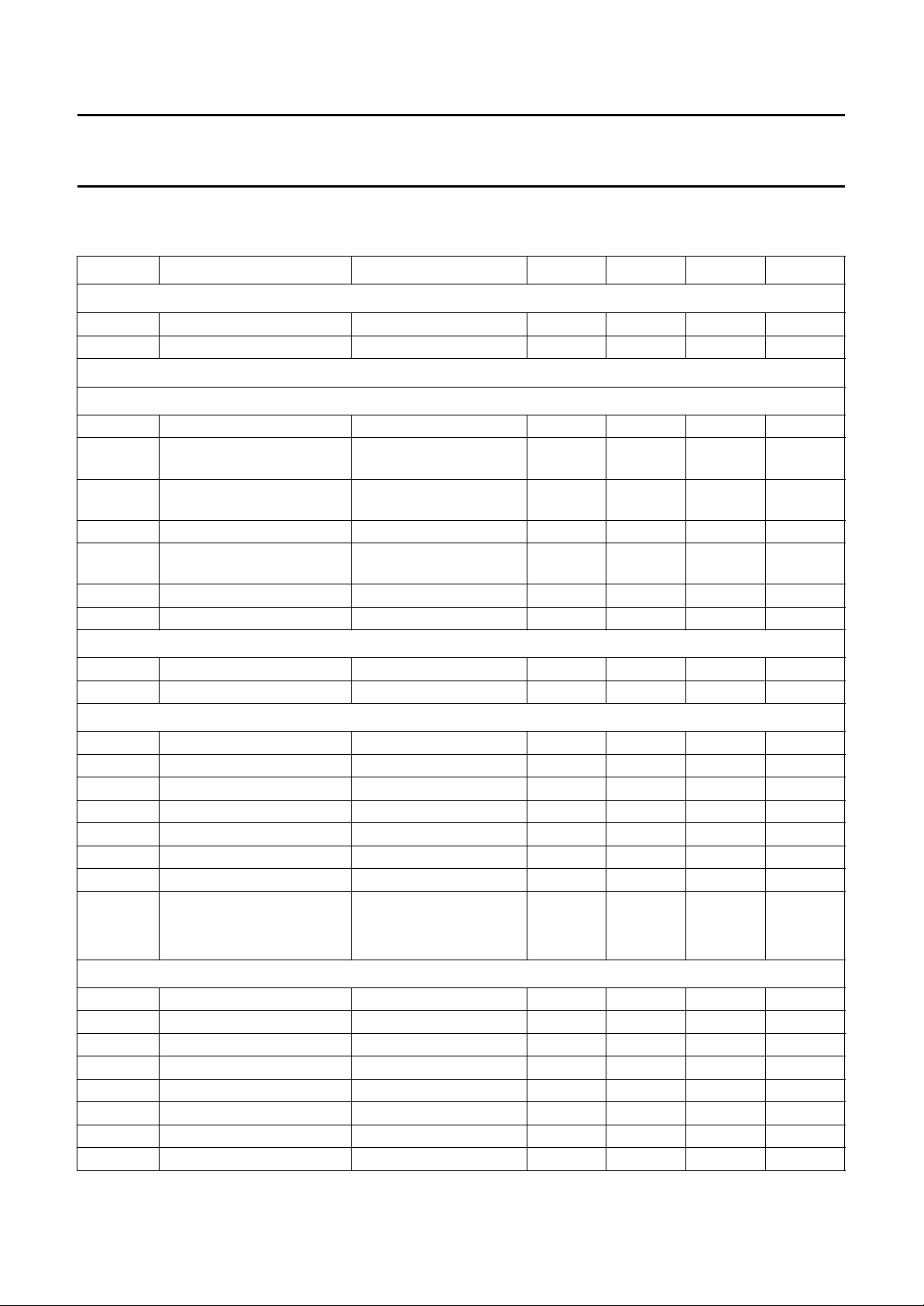
LIMITING VALUES
In accordance with the Absolute Maximum Rating System (IEC 134).
SYMBOL PARAMETER CONDITIONS MIN. MAX. UNIT
V
DD
V
Imax
V
Omax
V
dif
I
IOK
I
Omax
T
amb
T
stg
V
es
supply voltage (all supplies) −0.3 +6.5 V
maximum input voltage (any input) note 1 −0.3 VDD+ 0.5 V
maximum output voltage (any output) note 1 − VDD+ 0.5 V
difference between VSS and OSCGND −±0.25 V
DC input or output diode current −±20 mA
maximum output current (each output) −±10 mA
operating ambient temperature −20 +70 °C
storage temperature −55 +125 °C
electrostatic handling
human body model note 2 −2000 +2000 V
machine model note 3 −200 +200 V
Notes
1. This maximum value has an absolute maximum of 6.5 V independent of V
DD
.
2. The human body model ESD simulation is equivalent to discharging a 100 pF capacitor via a 1.5 kΩ resistor, which
produces a single discharge transient. Reference
to MIL-STD 883C method 3015.7)”
.
“Philips Semiconductors Test Method UZW-BO/FQ-A302 (similar
3. The machine model ESD simulation is equivalent to discharging a 200 pF capacitor via a resistor and series inductor
with effective dynamic values of 25 Ω and 2.5 µH, which produces a damped oscillating discharge. Reference
“Philips Semiconductors Test Method UZW-BO/FQ-B302 (similar to EIAJ IC-121 Test Method 20 condition C)”
.
Quality
This device will meet the requirements of the
in accordance with
“Quality Reference Handbook (order number 9397 750 00192)”
“Philips Semiconductors General Quality Specification UZW-BO/FQ-0601”
. This details the acceptance criteria
for all Q & R tests applied to the product.
1996 Jul 18 5
Philips Semiconductors Product specification
Line twenty-one acquisition and display (LITOD) SAA5252
CHARACTERISTICS
V
= 5 to 5.5 V; VSS=0V; T
DD
SYMBOL PARAMETER CONDITIONS MIN. TYP. MAX. UNIT
Supplies
V
DD
I
DDtot
supply voltage 4.5 5.0 5.5 V
total supply current − 30 − mA
Inputs
= −20 to +70 °C; unless otherwise specified.
amb
CVBS (
V
V
V
Z
V
Z
C
PIN 1)
syn
vid(p-p)
dat
source
I
I
I
IREF (PIN 24)
R
24
V
24
H(PIN 8)
V
IL
V
IH
I
LI
I
Imax
C
I
t
r
t
f
t
W
PIN 7)
V(
V
IL
V
IH
I
LI
I
Imax
C
I
t
r
t
f
t
W
sync voltage amplitude 0.1 0.3 0.6 V
video voltage amplitude
0.7 1.0 1.4 V
(peak-to-peak value)
caption data voltage
0.25 0.35 0.49 V
amplitude
source impedance −−250 Ω
input switching voltage level
1.7 2.0 2.3 V
of sync separator
input impedance 2.5 5 − kΩ
input capacitance −−10 pF
resistor to ground − 27 − kΩ
voltage on pin 24 −
1
⁄2V
DD
− V
LOW level input voltage −0.3 − +0.8 V
HIGH level input voltage 2.0 − VDD+ 0.5 V
input leakage current VI=0toV
DD
−10 − +10 µA
maximum input current −1 − +1 mA
input capacitance −−10 pF
pulse rise time −−5µs
pulse fall time −−5µs
pulse width
scan mode 1H 1 12 63 µs
scan mode 2H 1 6 31 µs
LOW level input voltage −0.3 − +0.8 V
HIGH level input voltage 2.0 − VDD+ 0.5 V
input leakage current VI=0toV
DD
−10 − +10 µA
maximum input current −1 − +1 mA
input capacitance −−10 pF
pulse rise time −−5ns
pulse fall time −−5ns
pulse width 1 −−µs
1996 Jul 18 6
 Loading...