

Philips SAA5250P, SAA5250T Datasheet

INTEGRATED CIRCUITS
DATA SH EET
SAA5250
Interface for data acquisition and
control
(for multi-standard teletext
systems)
Product specification
File under Integrated Circuits, IC02
January 1987

Philips Semiconductors Product specification
Interface for data acquisition and control
SAA5250
(for multi-standard teletext systems)
GENERAL DESCRIPTION
The SAA5250 is a CMOS Interface for Data Acquisition and Control (CIDAC) designed for use in conjunction with the
Video Input Processor (SAA5230) in a multi-standard teletext decoder. The device retrieves data from a user selected
channel (channel demultiplexer), as well as providing control signals and consecutive addressing space necessary to
drive a 2 K bytes buffer memory.
The system operates in accordance with the following transmission standards:
• French Didon Antiope specification D2 A4-2 (DIDON)
• North American Broadcast Teletext specification (NABTS)
• U.K. teletext (CEEFAX)
Features
• 7,5 MHz maximum conversion rate
• Three prefixes; DIDON, NABTS and U.K. teletext (CEEFAX)
• Mode without prefix
• Internal calculation of the validation (VAL) and colour burst blanking (CBB) signals, if programmed
• Programmable framing code and channel numbers
• Error parity calculation or not (odd parity)
• Hamming processing of the prefix byte
• Full channel or VBI reception
• Slow/fast mode (detection of page flags or not)
• Maximum/default format up to 63 bytes
• Addressing space of 2 K bytes of the static memory
• Multiplexed address/data information is compatible with Motorola or Intel microcontrollers
• CIDAC is ‘MOTEL’ compatible
PACKAGE OUTLINES
SAA5250P: 40-lead DIL; plastic (SOT129); SOT129-1; 1996 December 02.
SAA5250T: 40-lead mini-pack; plastic (VSO40); SOT158-1; 1996 December 02.
January 1987 2
Philips Semiconductors Product specification
Interface for data acquisition and control
(for multi-standard teletext systems)
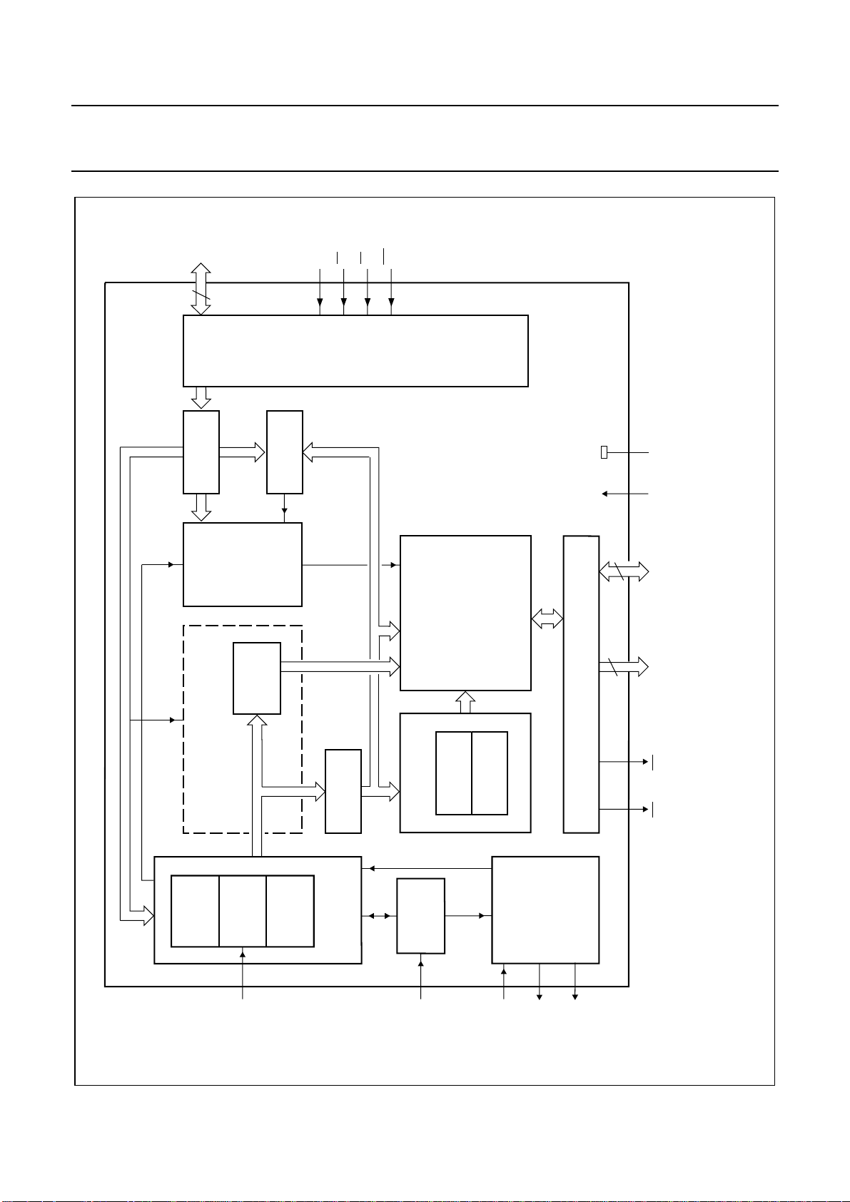
DB7toDB0
8
9-16
REGISTER
PROGRAM
17
CHANNEL
COMPARATOR
ALE
CS
RD
WR
18
21
19
INTERFACE
SAA5250
MGH075
SS
V
DD
SAA5250
, full pagewidth
PAGE DETECTION
CODE
FRAMING
DETECTION
SEQUENCE
CONTROLLER
REGISTER
SERIAL
REGISTER
PARALLEL
REGISTER
HAMMING
CORRECTOR
CONVERTER
SERIAL/PARALLEL
FORMAT
FORMAT
PROCESSOR
CLOCK
GENERATION
2 K BYTE
CONTROLLER
FIFO MEMORY
FORMAT
COUNTER
TRANSCODER
SIGNAL
VALIDATION
PROCESSING
29-22 40 20
8
1, 39-30
11
Fig.1 Block diagram.
MEMORY INTERFACE
WE A10 to A0 D7 to D0 V
78
MS
6
SD
January 1987 3
5
DCK
3
VAL IN/
SYNC
2
4
CBB
VAL OUT
Philips Semiconductors Product specification
Interface for data acquisition and control
(for multi-standard teletext systems)
handbook, halfpage
VAL OUT
VAL IN/
A10
SYNC
CBB
DCK
SD
MS
WE
DB7
DB6
DB5
DB4
DB3
DB2
DB1
DB0
ALE
CS
WR
V
SS
1
2
3
4
5
6
7
8
9
10
11
12
13
14
15
16
17
18
19
20
SAA5250
MGH074
SAA5250
40
V
DD
39
A9
38
A8
37
A7
36
A6
35
A5
34
A4
33
A3
32
A2
31
A1
30
A0
29
D7
28
D6
27
D5
26
D4
25
D3
24
D2
23
D1
22
D0
21
RD
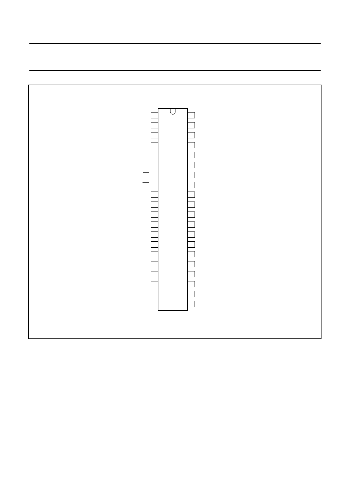
Fig.2 Pinning diagram.
January 1987 4

Philips Semiconductors Product specification
Interface for data acquisition and control
SAA5250
(for multi-standard teletext systems)
PINNING FUNCTION
MNEMONIC PIN NO. FUNCTION
A10 and
A0 to A9
VAL OUT 2 Validation output signal used to control the location of the window for the framing code.
VAL IN/SYNC 3 Validation input signal (line signal) used to give or calculate a window for the framing
CBB 4 Colour burst blanking output signal used by the SAA5230 as a data slicer reset pulse
DCK 5 Data clock input, in synchronization with the serial data signal
SD 6 Serial data input, arriving from the demodulator
MS 7 Chip enable output signal for buffer memory selection
WE 8 Write command output for the buffer memory
DB7 to DB0 9 to 16 8-bit three state input/output data/address bus used to transfer commands, data and
ALE 17 Demultiplexing input signal for the CPU data bus
CE 18 Chip enable input for the SAA5250
WR 19 Write command input (when LOW)
V
SS
RD 21 Read command input (when LOW)
D0 to D7 22 to 29 8-bit three state input/output data bus used to transfer data between CIDAC and the
V
DD
1 and
30 to 39
20 ground
40 +5 V power supply
Memory address outputs used by CIDAC to address a 2 K byte buffer memory
code detection
status between the CIDAC registers and the CPU
buffer memory
January 1987 5
Philips Semiconductors Product specification
Interface for data acquisition and control
SAA5250
(for multi-standard teletext systems)
FUNCTIONAL DESCRIPTION
Microcontroller interface
The microcontroller interface communicates with the CPU via the handshake signals DB7 − DB0, ALE, CS,
microcontroller interface produces control commands as well as programming the registers to write their contents or read
incoming status/data information from the buffer memory. The details of the codes used to address the registers are
given in Table 2.
The CIDAC is ‘MOTEL’ compatible (MOTEL compatible means it is compatible with standard Motorola or Intel
microcontrollers). It automatically recognizes the microcontroller type (such as the 6801 or 8501) by using the ALE signal
to latch the state of the RD input. No external logic is required.
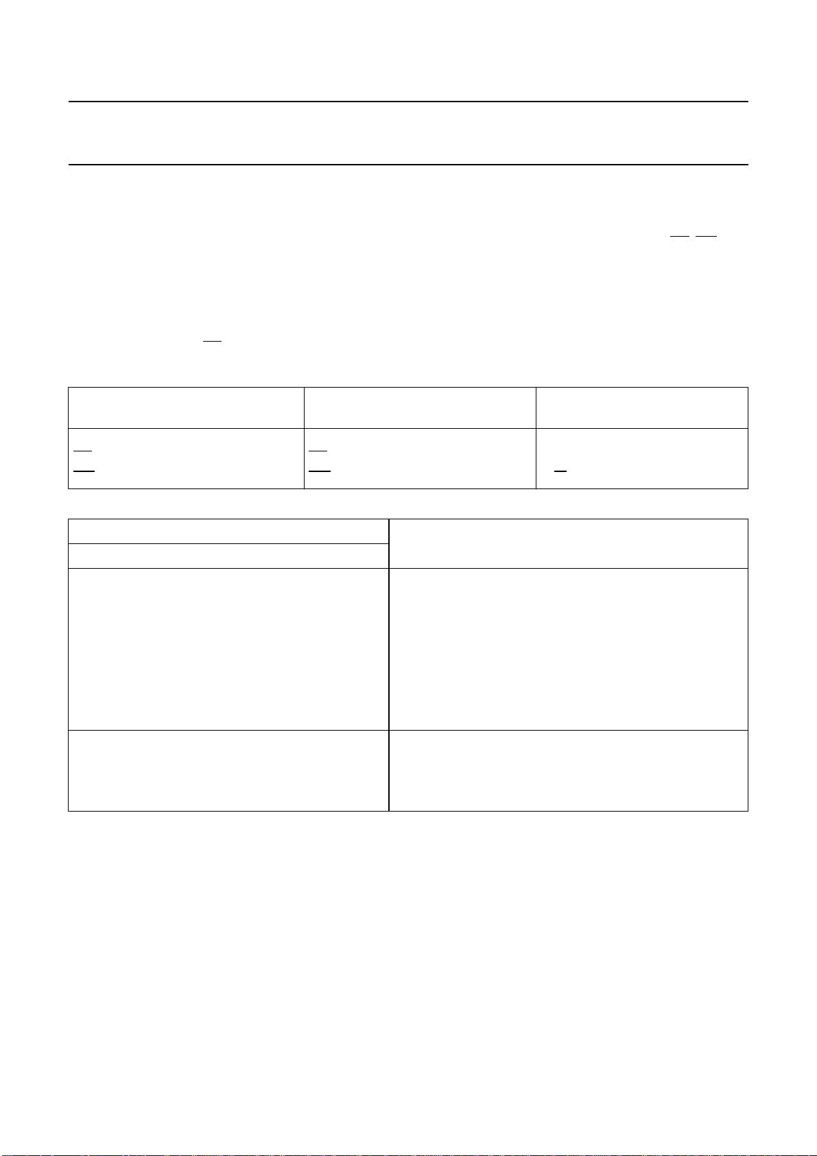
Table 1 Recognition signals
8049/8051
CIDAC
ALE ALE AS
RD RD DS, E, Φ 2
WR WR R/W
Table 2 CIDAC register addressing
TIMING 1
6801/6805
TIMING 2
RD,WR. The
CODES
FUNCTIONR W CS DB2 DB1 DB0
100000write register R0
100001write register R1
100010write register R2
100011write register R3
100100write register R4
100101write register R5
100110write command register R6 (initialization command)
100111write register R7
010000read status
010001read data register
010010test (not used)
010011test (not used)
January 1987 6
Philips Semiconductors Product specification
Interface for data acquisition and control
(for multi-standard teletext systems)
Register organization
R0 register
Table 3 R0 Register contents
R04
SLOW/FAST MODE
0 = slow mode 0 = no parity control 000 = DIDON long
1 = fast mode 1 = odd parity 001 = DIDON medium
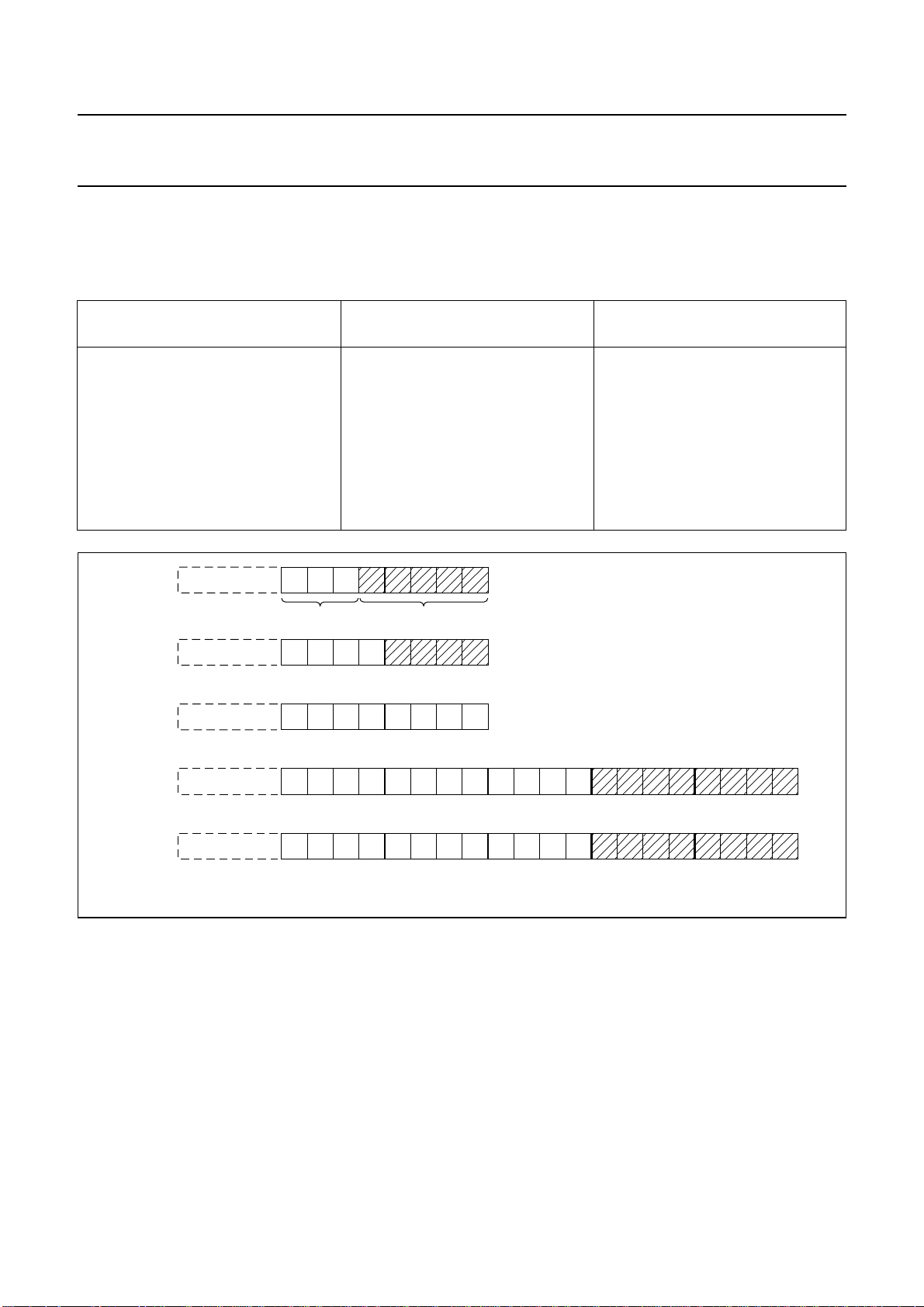
handbook, full pagewidth
FCCEEFAX
R03
PARITY
SAA5250
R02 TO R00
USED PREFIXES
010 = DIDON short
011 = not used
100 = U.K. teletext
101 = NABTS
110 = without prefix
111 = without prefix
magazine and row address group
MRAG
format
A2
A2
A2
A3
A3
CI
CI
format
PS
MGH077
DIDON
short
DIDON
medium
DIDON
long
NABTS
A
FC
A1
FC
A1
FC
A1
FC
Fig.3 Five prefixes.
All of the bytes (see Fig.3) are Hamming protected. The hatched bytes are always stored in the memory in order to be
processed by the CPU (see section ‘Prefix processing’). In the mode without prefix all of the bytes which follow the
framing code are stored in the memory until the end of the data packet, the format is then determined by the contents of
the R3 register.
If R03 = 0; no parity control is carried out and the 8-bits of the incoming data bytes are stored in the fifo memory.
If R03 = 1; the 8th bit of the bytes following the prefix (data bytes) represents the result of the odd parity control.
If R04 = 0; the device operates in the slow mode. The CIDAC retrieves data from the user selected magazine (see
section ‘R1 and R2’) and without searching for a start to a page stores the data into the FIFO memory.
January 1987 7
Philips Semiconductors Product specification
Interface for data acquisition and control
SAA5250
(for multi-standard teletext systems)
If R04 = 1; the device operates in the fast mode. Prior to writing into the FIFO memory, the CIDAC searches for a start
to a page which is variable due to the different prefixes:
• DIDON (long, medium and short): using the redundant bytes, SOH RS, X RS and SOH X (where X is a bit affected by
a parity error)
• NABTS, the least significant bit of the PS byte is set to 1
• U.K. teletext, ROW = 0
R1 register
Table 4 R1 Register contents
R17
VAL IN/SYNC
1 = VAL 000 = list 1 first digit hexadecimal value
0 = SYNC 001 = list 2
Note
1. X = don’t care
R16 TO R14
FORMAT TABLE
010 = list 3
011 = list 4
1XX = maximum/default value used (R3)
(1)
R13 TO R10
CHANNEL NUMBERS (FIRST DIGIT)
If VAL IN/SYNC = 1; the line signal immediately produces a validation signal for the framing code detection.
If VAL OUT = 0; the line signal is used as a starting signal for an internally processed validation signal (see Fig.15). The
framing code window width is fixed at 13 clock periods and the delay is determined by the contents of the R5 register
(R56 to R50).
At any moment the user is able to ensure that the framing code window is correctly located. This is accomplished by the
VAL OUT pin reflecting the internal validation signal. A CBB signal with programmable width (see section ‘R7 register’)
can also be generated, this is used as a data slicer reset pulse by the SAA5230. The line signal is used as the starting
point of the internal CBB signal width fixed by the contents of the R7 register.
If R16 = 0; then bits R15 and R14 provide the format table number using DIDON long and short prefixes (see Table 6).
If R16 = 1; then the format is determined by the contents of the R3 register.
The bits R13 to R10 represent the first channel number to be checked in the prefix. In U.K. teletext mode only 3 bits are
required, so R13 = X.
January 1987 8
Philips Semiconductors Product specification
Interface for data acquisition and control
(for multi-standard teletext systems)
Table 5 Format table
FORMAT BYTE
B8, B6, B4 AND B2
0000 0 0 0 0
0001 1 1 1 1
0010 2 2 2 2
0011 3 3 3 3
0100 4 5 6 7
0101 8 9 10 11
0110 12 13 14 15
0111 16 17 18 19
1000 20 21 22 23
1001 24 25 26 27
1010 28 29 30 31
1011 3233 3435
1100 36 37 38 39
1101 40 41 42 43
1110 44 45 46 47
1111 48 49 50 51
(1)
LIST 1 LIST 2 LIST 3 LIST 4
SAA5250
Note
1. B8 = MSB and B2 = LSB.
R2 register
Table 6 R2 Register contents
R27 TO R24 R23 TO R20
channel number, third digit channel number, second digit
(hexadecimal value, third digit) (hexadecimal value, second digit
Note
1. R27 and R23 = MSB and R24 and R20 = LSB
The R2 register provides the other two parts of the channel number (depending on the prefix) that require checking.
January 1987 9
Philips Semiconductors Product specification
Interface for data acquisition and control
SAA5250
(for multi-standard teletext systems)
R3 register
Table 7 R3 register contents
R35 TO R30
6-BIT FORMAT MAXIMUM/DEFAULT VALUE
000000 = 0
000001 = 1
−
−
−
111111 = 63
This 6-bit byte gives:
• In the DIDON long and short mode, a maximum format in case of corrupted transmission (multiple errors on the
Hamming corrector)
• A possible 63-bit format for all types of prefix
R4 register
Table 8 R4 register contents
R47 TO R40
8-bit register used for storing the framing code value which will be compared with the third byte of each data
line
R5 register
Table 9 R5 register contents
R57
NEGATIVE/POSITIVE
0 = negative edge for sync signal 7-bit sync delay, giving a maximum
1 = positive edge for sync signal delay of (2
Note
1. F = data clock acquisition frequency (DCK).
Using R57 it is possible to start the internal synchronization delay (t
R6 write command register
This is a fictitious register. Only the address code (see Table 2) is required to reset the CIDAC. See Table 11 for the
status of the FIFO memory on receipt of this command.
R7 register
Table 10 R7 register contents
R56 TO R50
SYNCHRONIZATION DELAY
7
− 1) × 106µs/F (Hz)
) on the positive or negative edge.
DVAL
R75 TO R70
6-bit register used to give a maximum colour burst blanking signal of: (26− 1) × 106µs/F (Hz)
Note
1. F = data clock acquisition frequency.
January 1987 10

Philips Semiconductors Product specification
Interface for data acquisition and control
SAA5250
(for multi-standard teletext systems)
Fifo status register (
Table 11 Fifo register contents
DB2 TO DB0
DB2 = 1
memory empty
Once the relevant prefix and the right working modes have been given by the corresponding registers, a write command
to the R6 register enables the CIDAC to accept and process serial data.
Channel comparator
This is a four bit comparator which compares the three user hexadecimal defined values in R1 and R2 to corresponding
bytes of the prefix coming from the Hamming corrector. If the three bytes match, the internal process of the prefix
continues. If they do not match the CIDAC returns to a wait state until the next broadcast data package is received.
FIFO memory controller
The FIFO memory contains all the necessary functions required for the control of the 11-bit address memory (2 K byte).
The functions contained in the FIFO memory are as follows:
• write address register (11-bits)
• read address register (11-bits)
• memory pointer (11-bits)
• address multiplexer (11-bits)
• write data register (8-bits)
• read data register (8-bits)
• data multiplexer
• control logic
read R0 register)
DB1 = 1, data not present in the
read data register
DB0 = 0
memory not full
The FIFO memory provides the memory interface with the following:
• 11-bit address bus (A10 to A0)
• 8-bit data bus (D7 to D0)
• two control signals, memory select (MS) and write enable (WE)
January 1987 11
 Loading...