

Philips saa5249 DATASHEETS

INTEGRATED CIRCUITS
DATA SH EET
SAA5249
Integrated VIP and Teletext with
Background Memory Controller
(IVT1.1BMCX)
Preliminary specification
Supersedes data of December 1993
File under Integrated Circuits, IC02
1996 Nov 07

Philips Semiconductors Preliminary specification
Integrated VIP and Teletext with
Background Memory Controller
FEATURES
• Complete teletext decoder featuring a background
memory controller in a single 48-pin DIP package.
Capable of storing of up to 512 teletext pages in an
external DRAM, giving instant access to the teletext
data
• Automatic processing of extension packet 26 for widest
possible language decoding. All our standard language
options can be available, and the language option is
readable via I2C-bus.
• 100% hardware compatible with the SAA5247 plug-in
replacement and with the possibility of extra market in
those countries with packet 26 transmissions.
Still pin-aligned to SAA5254 and SAA5244A.
• 100% software compatible with the SAA5247, and
SAA5244A, except if the special OSD symbols were
used. Also 100% software compatible to SAA5254. In all
events there is a change to the ROM ID number.
• The device is pin-aligned with the other members of the
new Philips teletext decoder family, i.e. SAA5281 and
the SAA5254, making one hardware solution for the
whole range
• Low software overhead for the microprocessor
• RGB interface to standard colour decoder ICs, push-pull
output drive.
GENERAL DESCRIPTION
The Integrated VIP and Teletext (IVT1.1BMCX) is a
teletext decoder (contained within a single chip package)
for decoding 625-line based World System Teletext
transmissions. With its built-in background memory
controller the device can store incoming teletext packets in
the external 1M4 DRAM. With this large packet store
which can be rapidly scanned, we can achieve near
instantaneous access to all the pages transmitted by the
broadcaster.
This version of the decoder also contains some extra
hardware to process extension packet 26 automatically,
extending the markets to which the TV chassis can be
shipped and offering many more language options for the
set maker.
SAA5249
QUICK REFERENCE DATA
SYMBOL PARAMETER MIN. TYP. MAX. UNIT
V
DD
I
DD
V
syn
V
vid
f
XTAL
T
amb
supply voltage 4.5 5.0 5.5 V
supply current − 90 120 mA
sync amplitude 0.1 0.3 0.6 V
video amplitude 0.7 1.0 1.4 V
crystal frequency − 27 − MHz
operating ambient temperature −20 − +70 °C
ORDERING INFORMATION
TYPE
NUMBER
NAME DESCRIPTION VERSION
PACKAGE
SAA5249P/E DIP48 plastic dual in-line package; 48 leads (600 mil) SOT240-1
SAA5249GP/E QFP64 plastic quad flat package; 64 leads (lead length 1.95 mm);
SOT319-1
body 14 × 20 × 2.7 mm; high stand-off height
1996 Nov 07 2
Philips Semiconductors Preliminary specification
Integrated VIP and Teletext with
Background Memory Controller
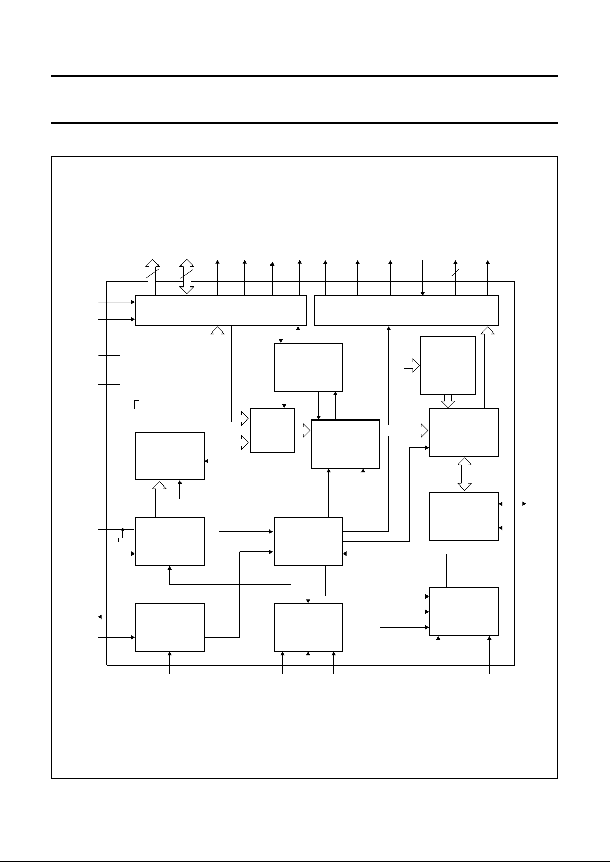
BLOCK DIAGRAM
SAA5249
handbook, full pagewidth
DD1
DD2
SSn
SS1
46
45
3
12
16, 22
38
7
8
SEL1
SEL2
V
V
V
V
REF+
A0 to A9 D0 to D3
10
4
SAA5249
DATA SLICER
AND
CLOCK
REGENERATOR
DCVBS
ANALOG
TO
DIGITAL
CONVERTER
42
23
DRAM INTERFACE
RASR/W CAS1 ODD/EVEN
24 41
BACKGROUND
MUX
MEMORY
CONTROL
TIMING
CHAIN
29
TELETEXT
ACQUISITION
AND
DECODING
COR
21 27
DISPLAY
R/G/BY BLANK RGBREFCAS0
3
20 17 to 19 28
HAMMING
CHECKER
AND
PACKET 26
PROCESSING
ENGINE
MEMORY
2
I C - BUS
INTERFACE
PAGE
31
SDA
30
SCL
OSCOUT
OSCIN
4
CRYSTAL
5
OSCILLATOR
6
GNDO
INPUT CLAMP
SYNC
SEPARATOR
911
BLACK IREF STTV/LFBPOL
Fig.1 Block diagram for SOT240-1 (DIP48) package.
1996 Nov 07 3
AND
DISPLAY
CLOCK
PHASE
LOCKED
LOOP
10 13 15 14
CVBS
VCR/FFB
MLB304
Philips Semiconductors Preliminary specification
Integrated VIP and Teletext with
Background Memory Controller
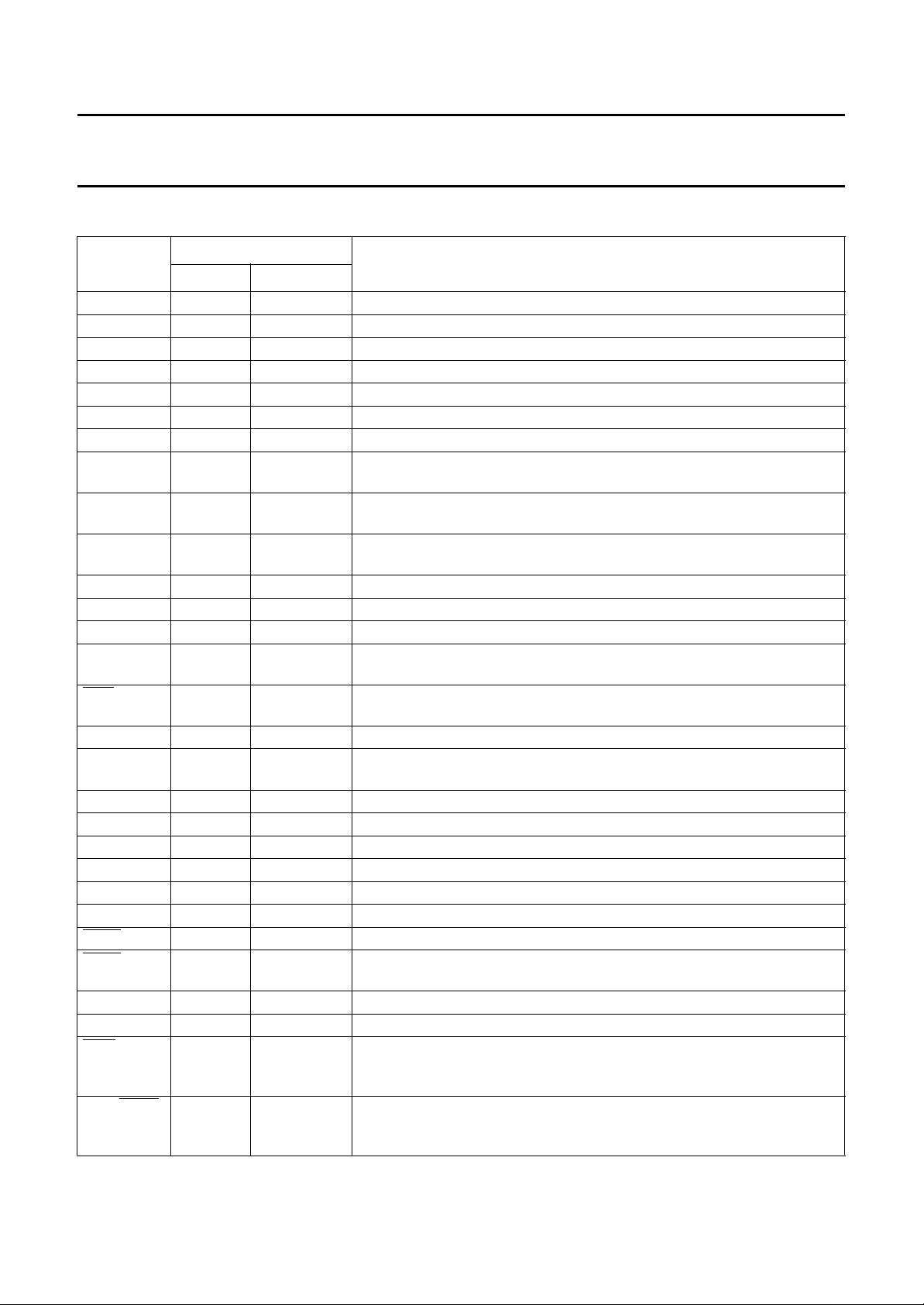
PINNING
SAA5249
SYMBOL
SOT240-1 SOT319-1
(1)
DESCRIPTION
n.c. 1 1 not connected
n.c. 2 2 not connected
PIN
V
DD1
3 25 +5 V supply
OSCOUT 4 27 27 MHz crystal oscillator output
OSCIN 5 28 27 MHz crystal oscillator input
GNDO 6 29 0 V crystal oscillator ground
V
SS1
7 12 0 V ground
REF+ 8 32 positive reference voltage; this pin should be connected to ground via a
100 nF capacitor
BLACK 9 35 video black level storage pin; this pin should be connected to ground via a
100 nF capacitor
CVBS 10 36 composite video input pin; a positive-going 1 V (p-p) input is required,
connected via a 100 nF capacitor
IREF 11 37 reference current input pin; connected to ground via a 27 kΩ resistor
V
DD2
12 38 +5 V supply
POL 13 39 STTV/LFB/FFB polarity selection pin
STTV/LFB 14 40 sync to TV output pin/line flyback input pin; function controlled by an
internal register bit (scan sync mode)
VCR/FFB 15 42 PLL time constant switch/field input pin; function controlled by an internal
register bit (scan sync mode)
V
SS2
16 30 0 V ground
REF−−31 negative reference voltage; this pin should be connected to REF+ via a
100 nF capacitor
R 17 49 dot rate character output of the RED colour information
G 18 50 dot rate character output of the GREEN colour information
B 19 51 dot rate character output of the BLUE colour information
RGBREF 20 52 input DC voltage to define the output high level on the RGB pins
BLANK 21 53 dot rate fast blanking output
V
SS3
22 54, 55 0 V ground; internally connected for SOT319
CAS0 23 56 column address select to external DRAM for BMCX function
CAS1 24 57 column address select to external DRAM for BMCX function for second
DRAM where two 256 k × 4 devices are used
A4 25 58 address output to external DRAM for BMCX function
A3 26 59 address output to external DRAM for BMCX function
COR 27 60 programmable output to provide contrast reduction of the TV picture for
mixed text and picture displays or when viewing newsflash/subtitle pages;
open drain output
EVEN 28 61 25 Hz output synchronized with the CVBS input field sync pulses to
ODD/
produce a non-interlaced display by adjustment of the vertical deflection
currents
1996 Nov 07 4

Philips Semiconductors Preliminary specification
Integrated VIP and Teletext with
Background Memory Controller
SAA5249
SYMBOL
Y 29 62 dot rate character output of teletext foreground colour information; open
SCL 30 63 serial clock input for I2C-bus; it can still be driven HIGH during power-down
SDA 31 64 serial data port for the I
A5 32 4 address output to external DRAM for BMCX function
A2 33 5 address output to external DRAM for BMCX function
A6 34 6 address output to external DRAM for BMCX function
A1 35 8 address output to external DRAM for BMCX function
A7 36 9 address output to external DRAM for BMCX function
A0 37 11 address output to external DRAM for BMCX function
V
SS4
A8 39 13 address output to external DRAM for BMCX function
A9 40 14 address output to external DRAM for BMCX function
RAS 41 15 row address select to external DRAM
W 42 18 read/write for external DRAM
R/
D2 43 19 data input/output for external DRAM
D0 44 20 data input/output for external DRAM
SEL2 45 21 RAM select input to choose external DRAM size
SEL1 46 22 RAM select input to choose external DRAM size
D3 47 23 data input/output for external DRAM
D1 48 24 data input/output for external DRAM
SOT240-1 SOT319-1
38 43 0 V ground
PIN
(1)
drain output
of the device
2
C-bus; open drain output. It can still be driven
HIGH during power-down of the device
DESCRIPTION
Note
1. The remaining pins for SOT319 are not connected.
1996 Nov 07 5
Philips Semiconductors Preliminary specification
Integrated VIP and Teletext with
Background Memory Controller
V
DD1
OSCOUT
OSCIN
n.c.
n.c.
48
1
2
3
4
5
D1
47
D3
SEL1
46
45
SEL2
D0
44
SAA5249
GNDO
V
SS1
REF
BLACK
CVBS
IREF
V
DD2
POL
STTV/LFB
VCR/FFB
V
SS2
RGBREF
BLANK
V
SS3
CAS0
CAS1
43
42
41
40
39
38
37
36
35
34
33
32
31
30
29
28
27
26
25
D2
R/W
RAS
A9
A8
V
SS4
A0
A7
A1
A6
A2
A5
SDA
SCL
Y
ODD/EVEN
COR
A3
A4
6
7
8
9
10
11
12
SAA5249P
13
14
15
16
17
R
18
G
B
19
20
21
22
23
24
MLB305
Fig.2 Pin configuration; SOT240-1 (DIP48).
1996 Nov 07 6

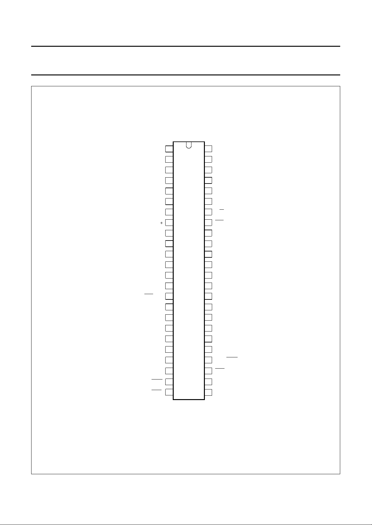
Philips Semiconductors Preliminary specification
Integrated VIP and Teletext with
Background Memory Controller
index
corner
n.c.
n.c.
n.c.
A5
A2
A6
n.c.
A1
A7
n.c.
A0
V
SS1
A8
A9
RAS
n.c.
n.c.
R/W
D2
SDA
64
1
2
3
4
5
6
7
8
9
10
11
12
13
14
15
16
17
18
19
SCL
63
Y
62
ODD/EVEN
61
COR
A3
60
59
SAA5249GP
A4
58
CAS1
57
CAS0
56
SS3
V
55
SS3
V
54
BLAN
53
RGBREF
52
51
50
49
48
47
46
45
44
43
42
41
40
39
38
37
36
35
34
33
B
G
R
n.c.
V
SS4
VCR/FFB
n.c.
STTV/LFB
POL
V
DD2
IREF
CVBS
BLACK
n.c.
n.c.
SAA5249
20
21
D0
SEL2
22
SEL1
23
D3
24
D1
25
V
DD1
26
n.c.
Fig.3 Pin configuration; SOT319-1 (QFP64).
1996 Nov 07 7
27
28
OSCIN
OSCOUT
29
GNDO
30
SS2
V
31
REF
32
REF
MLB306
Philips Semiconductors Preliminary specification
Integrated VIP and Teletext with
Background Memory Controller
LIMITING VALUES
In accordance with Absolute Maximum Rating System (IEC 134).
SYMBOL PARAMETER MIN. MAX. UNIT
V
DD
V
I
V
O
I
O
I
IOK
T
amb
QUALITY AND RELIABILITY
supply voltage (all supplies) −0.3 +6.5 V
input voltage (any input) −0.3 VDD+ 0.5 V
output voltage (any output) −0.3 VDD+ 0.5 V
output current (each output) −±10 mA
DC input or output diode current −±20 mA
operating ambient temperature −20 +70 °C
SAA5249
This device will meet Philips Semiconductors General Quality Specification for Business group
Circuits SNW-FQ-611-Part E”
. The principal requirements are shown in Tables 1 to 4.
“Consumer Integrated
1996 Nov 07 8
Philips Semiconductors Preliminary specification
Integrated VIP and Teletext with
Background Memory Controller
Group A
Table 1 Acceptance tests per lot
TEST REQUIREMENTS
Mechanical cumulative target: <100 ppm
Electrical cumulative target: <100 ppm
Group B
Table 2 Processability tests (by package family)
TEST REQUIREMENTS
Solderability <7% LTPD
Mechanical <15% LTPD
Solder heat resistance <15% LTPD
Group C
SAA5249
(1)
(1)
Table 3 Reliability tests (by process family)
TEST CONDITIONS REQUIREMENTS
(1)
Operational life 168 hours at Tj= 150 °C <1500 FPM; equivalent to <100 FITS
at Tj=70°C
Humidity life temperature, humidity, bias
<2000 FPM
(1000 hours, 85 °C, 85% RH or
equivalent test)
Temperature cycling performance T
stg(min)
to T
stg(max)
<2000 FPM
Table 4 Reliability tests (by device type)
TEST CONDITIONS REQUIREMENTS
ESD and latch-up ESD Human body model
<15% LTPD
(1)
2000 V, 100 pF, 1.5 kΩ
ESD Machine model
<15% LTPD
200 V, 100 pF, 1.5 kΩ
latch-up 100 mA, 1.5 × V
DD
<15% LTPD
(absolute maximum)
Note to Tables 1 to 4
1. ppm = fraction of defective devices, in parts per million.
LTPD = Lot Tolerance Percent Defective.
FPM = fraction of devices failing at test condition, in Failures Per Million.
FITS = Failures In Time Standard.
1996 Nov 07 9
Philips Semiconductors Preliminary specification
Integrated VIP and Teletext with
Background Memory Controller
CHARACTERISTICS
V
=5V±10%; T
DD
SYMBOL PARAMETER CONDITIONS MIN. TYP. MAX. UNIT
Supplies
V
DD
I
DD(tot)
supply voltage 4.5 5.0 5.5 V
total supply current − 90 120 mA
Inputs
CVBS
V
sync
t
d(sync)
sync amplitude 0.1 0.3 0.6 V
delay from CVBS to TCS output
from STTV buffer (nominal video,
average of leading/trailing edge)
∆t
d(sync)
change in sync delay between all
black and all white video input at
nominal levels
V
vid(p-p)
video input amplitude
(peak-to-peak value)
display PLL catching range ±7 −−%
Z
source
C
i
source impedance −−250 Ω
input capacitance −−10 pF
IREF
R
gnd
resistor to ground − 27 − kΩ
POL
V
IL
V
IH
I
LI
C
i
LOW level input voltage −0.3 − +0.8 V
HIGH level input voltage 2.0 − VDD+ 0.5 V
input leakage current Vi= 0 to V
input capacitance −−10 pF
LFB
V
IL
V
IH
I
LI
I
i
t
d(LFB)
LOW level input voltage −0.3 − +0.8 V
HIGH level input voltage 2.0 − VDD+ 0.5 V
input leakage current Vi= 0 to V
input current note 1 −1 − +1 mA
delay between LFB front edge
and input video line sync
VCR/FFB
V
IL
V
IH
I
LI
I
i
LOW level input voltage −0.3 − +0.8 V
HIGH level input voltage 2.0 − VDD+ 0.5 V
input leakage current Vi= 0 to V
input current note 1 −1 − +1 mA
= −20 to +70 °C; unless otherwise specified.
amb
DD
DD
DD
−150 0 +150 ns
0 − 25 ns
0.7 1.0 1.4 V
−10 − +10 µA
−10 − +10 µA
− 250 − ns
−10 − +10 µA
SAA5249
1996 Nov 07 10
Philips Semiconductors Preliminary specification
Integrated VIP and Teletext with
Background Memory Controller
SYMBOL PARAMETER CONDITIONS MIN. TYP. MAX. UNIT
RGBREF note 2
V
IL
I
LI
I
DC
SEL1 AND SEL2
V
IL
V
IH
I
LI
SCL
V
IL
V
IH
I
LI
f
SCL
t
r
t
f
C
i
Inputs/outputs
LOW level input voltage −0.3 − VDD+ 0.5 V
input leakage current Vi= 0 to V
DD
−10 − +10 µA
DC current −−10 mA
LOW level input voltage −0.3 − +0.8 V
HIGH level input voltage 2.0 − VDD+ 0.5 V
input leakage current Vi= 0 to V
DD
−10 − +10 µA
LOW level input voltage −0.3 − +1.5 V
HIGH level input voltage 3.0 − VDD+ 0.5 V
input leakage current Vi= 0 to V
DD
−10 − +10 µA
clock frequency 0 − 100 kHz
input rise time 10% to 90% −−2µs
input fall time 90% to 10% −−2µs
input capacitance −−10 pF
SAA5249
C
RYSTAL OSCILLATOR (OSCIN; OSCOUT)
f
XTAL
G
v
G
m
C
i
C
FB
crystal frequency − 27 − MHz
small signal voltage gain 3.5 −−
mutual conductance fi= 100 kHz 1.5 −−mA/V
input capacitance −−10 pF
feedback capacitance −−5pF
BLACK
C
blk
I
LI
storage capacitor to ground − 100 − nF
input leakage current Vi= 0 to V
SDA
V
IL
V
IH
I
LI
C
i
t
r
t
f
V
OL
t
f
C
L
LOW level input voltage −0.3 − +1.5 V
HIGH level input voltage 3.0 − VDD+ 0.5 V
input leakage current Vi= 0 to V
input capacitance −−10 pF
input rise time 10% to 90% −−2µs
input fall time 90% to 10% −−2µs
LOW level output voltage IOL= 3 mA 0 − 0.5 V
output fall time 3 V to 1 V −−200 ns
load capacitance −−400 pF
DD
DD
−10 − +10 µA
−10 − +10 µA
1996 Nov 07 11
Philips Semiconductors Preliminary specification
Integrated VIP and Teletext with
Background Memory Controller
SYMBOL PARAMETER CONDITIONS MIN. TYP. MAX. UNIT
D0 TO D3
V
IL
V
IH
I
LI
C
i
V
OL
V
OH
t
r
t
f
C
L
Outputs
STTV
G
stt
V
TCS
V
DCs
I
O
C
L
A0 TO A9 ADDRESS OUTPUT TO MEMORY A0 TO A9
V
OL
V
OH
C
L
t
r
t
f
R/W, CASO AND CAS1
V
OL
V
OH
C
L
t
r
t
f
LOW level input voltage −0.3 − +0.8 V
HIGH level input voltage 2.0 − VDD+ 0.5 V
input leakage current −10 − +10 µA
input capacitance −−10 pF
LOW level output voltage IOL= +1.6 mA 0 − 0.4 V
HIGH level output voltage IOH= −0.2 mA 2.4 − V
output rise time 0.6 to 2.2 V −−20 ns
output fall time 2.2 to 0.6 V −−20 ns
load capacitance −−50 pF
gain of STTV relative to video
0.9 1.0 1.1
input
TCS amplitude 0.2 0.3 0.45 V
DC shift between TCS output and
−−0.15 V
nominal video output
output drive current −−3.0 mA
load capacitance −−100 pF
LOW level output voltage IOL= +1.6 mA 0 − 0.4 V
HIGH level output voltage IOH= −0.2 mA 2.4 − V
load capacitance −−50 pF
output rise time 0.6 to 2.2 V −−20 ns
output fall time 2.2 to 0.6 V −−20 ns
LOW level output voltage IOL= +1.6 mA 0 − 0.4 V
HIGH level output voltage IOH= −0.2 mA 2.4 − V
load capacitance −−50 pF
output rise time 0.6 to 2.2 V −−20 ns
output fall time 2.2 to 0.6 V −−20 ns
SAA5249
DD
DD
DD
V
V
V
1996 Nov 07 12
Philips Semiconductors Preliminary specification
Integrated VIP and Teletext with
Background Memory Controller
SYMBOL PARAMETER CONDITIONS MIN. TYP. MAX. UNIT
R, G AND B
V
OL
V
OH
| output impedance −−200 Ω
|Z
o
C
L
I
DC
t
r
t
f
BLANK
V
OL
V
OH
V
OH
V
OH
C
L
t
r
t
f
ODD/EVEN
V
OL
V
OH
C
L
t
r
t
f
COR AND Y(OPEN-DRAIN)
V
OH
V
OL
C
L
t
f
I
LO
t
skew
LOW level output voltage IOL= 2 mA 0 − 0.2 V
HIGH level output voltage IOH= −1.6 mA;
RGBREF ≤ VDD− 2V
RGBREF
−0.25
RGBREF RGBREF
load capacitance −−50 pF
DC current −−−3.3 mA
output rise time 10% to 90% −−20 ns
output fall time 90% to 10% −−20 ns
LOW level output voltage IOL= 1.6 mA 0 − 0.4 V
HIGH level output voltage IOH= −0.2 mA;
1.1 −−V
VDD= 4.5 V
HIGH level output voltage IOH= 0 mA;
−−2.8 V
VDD= 5.5 V
allowed voltage at pin with external pull-up −−VDDV
load capacitance −−50 pF
output rise time 10% to 90% −−20 ns
output fall time 90% to 10% −−20 ns
LOW level output voltage IOL= +1.6 mA 0 − 0.4 V
HIGH level output voltage IOH= −0.2 mA 2.4 − V
load capacitance −−120 pF
output rise time 0.6 to 2.2 V −−50 ns
output fall time 2.2 to 0.6 V −−50 ns
pull-up voltage at pin −−VDDV
output voltage LOW IOL= 5 mA 0 − 1.0 V
load capacitance −−25 pF
output fall time load resistor of 1.2 kΩ
−−50 ns
to VDD; measured
between VDD− 0.5 V
and 1.5 V
output leakage current Vi= 0 to V
skew delay between display
DD
−10 − +10 µA
−−20 ns
outputs R, G, B, COR, Y and
BLANK
SAA5249
+0.25
DD
V
V
1996 Nov 07 13
Philips Semiconductors Preliminary specification
Integrated VIP and Teletext with
Background Memory Controller
SYMBOL PARAMETER CONDITIONS MIN. TYP. MAX. UNIT
Timing
DRAM INTERFACE
t
RC
t
RP
t
RAS
t
CAS
t
ASR
t
RAH
t
ASC
t
CAH
t
RCD
t
RAD
t
RSH
t
CSH
t
CRP
t
DZO
, t
t
r
f
t
WCS
t
WCH
t
DS
t
DH
t
RAC
t
CAC
t
AA
t
RCS
t
RCH
t
RRH
t
RAL
t
OFF1
t
CDD
read or write cycle time 344 380 415 ns
RAS precharge time 125 140 155 ns
RAS pulse width 194 210 230 ns
CAS pulse width 113 133 153 ns
row address set-up time 30 60 80 ns
row address hold time 50 60 92 ns
column address set-up time 50 60 75 ns
column address hold time 50 60 70 ns
RAS to CAS delay time 130 148 160 ns
RAS to column address delay
60 74 105 ns
time
RAS hold time 15 60 70 ns
CAS hold time 260 286 300 ns
CAS to RAS precharge time 60 70 80 ns
CAS set-up time from data input 200 225 280 ns
rise and fall times 10 15 20 ns
write set-up time 193 212 235 ns
write command hold time 116 137 150 ns
data input set-up time 193 212 235 ns
data input hold time 42 62 80 ns
access time from RAS 165 183 220 ns
access time from CAS 0 3540ns
access time from address 95 108 120 ns
read command set-up time 193 212 235 ns
read command hold time to CAS 0 1020ns
read command hold time to RAS 55 65 100 ns
column address to RAS lead time 90 133 150 ns
output buffer turn-off time 20 30 40 ns
CAS to data input delay time 25 35 45 ns
SAA5249
1996 Nov 07 14
 Loading...