Philips saa5246a DATASHEETS

INTEGRATED CIRCUITS
DATA SH EET
SAA5246A
Integrated VIP and Teletext
(IVT1.0)
Product specification
Supersedes data of August 1992
File under Integrated Circuits, IC02
January 1993

Philips Semiconductors Product specification
Integrated VIP and Teletext (IVT1.0) SAA5246A
FEATURES
• Complete Teletext decoder in a 48-pin DIL or 64-pin
QFP, integrated circuit
• Single +5 V power supply
• Both video and scan related synchronization modes are
supported
• RGB interface to standard colour decoder ICs, push-pull
output drive
• Digital data slicer and display clock phase-locked loop
reduce peripheral components to a minimum
• Data capture performance similar to SAA5231 (VIP2)
• Option for up to seven national languages
• Optional storage of packet 24 in the display memory
• Separate text and video signal quality detectors,
625/525 video status and language version all readable
via I2C-bus
• Automatic ODD/EVEN output control with override
• Control of display PLL free-run and rolling header via
I2C-bus
• VCS to SCS mode for stable 525 line status display.
DESCRIPTION
The SAA5246A is a single-chip teletext decoder IC for
decoding 625 line base World System Teletext
transmissions. The teletext decoder hardware is based on
the Enhanced Computer Controlled ECCT device
(SAA5243) with some additional features.
The Video Input Processor section of the device uses
mixed analog and digital designs in the data slicer and
clock phase-locked-loop functions. As a result the number
of external components are greatly reduced and no critical
or adjustable components are required.
QUICK REFERENCE DATA
SYMBOL PARAMETER MIN. TYP. MAX. UNIT
V
DD
I
DD
V
syn
V
vid
f
XTAL
T
amb
positive supply voltage 4.5 5.0 5.5 V
supply current − 64 128 mA
sync amplitude 0.1 0.3 0.6 V
video amplitude 0.7 1.0 1.4 V
crystal frequency − 27 − MHz
operating ambient temperature −20 − +70 °C
ORDERING INFORMATION
EXTENDED TYPE
NUMBER
PINS PIN POSITION MATERIAL CODE
PACKAGE
SAA5246AP 48 DIL plastic SOT240AC3
SAA5246AGP 64 QFP plastic SOT319DA3
Notes
1. SOT240-1; 1996 November 22.
2. SOT319-3; 1996 November 22.
(1)
(2)
January 1993 2
Philips Semiconductors Product specification
Integrated VIP and Teletext (IVT1.0) SAA5246A
handbook, full pagewidth
REGENERATOR
DCVBS
Y
BLAN
22 19 20 18 15-17 21
DATA
SLICER
AND
CLOCK
ANALOG
TO
DIGITAL
CONVERTER
RGBREF RGB
DISPLAY
ODD / EVENCOR
TELETEXT
ACQUISITION
AND
DECODING
TIMING
CHAIN
MEMORY
INTERFACE
2
I
C-BUS
INTERFACE
SAA5246A
34-
26-
24
23
1, 6,
10
25
14
48
WE
47
OE
46
A0 - A12
D0 - D7
33
SDA
SCL
V
DD
V
5,
SS
CVBS
OSCOUT
OSCIN
2
3
CRYSTAL
OSCILLATOR
4 7 9 8 11 13 12
OSCGND BLACK IREF CVBS POL STTV / LFB
SEPARATOR
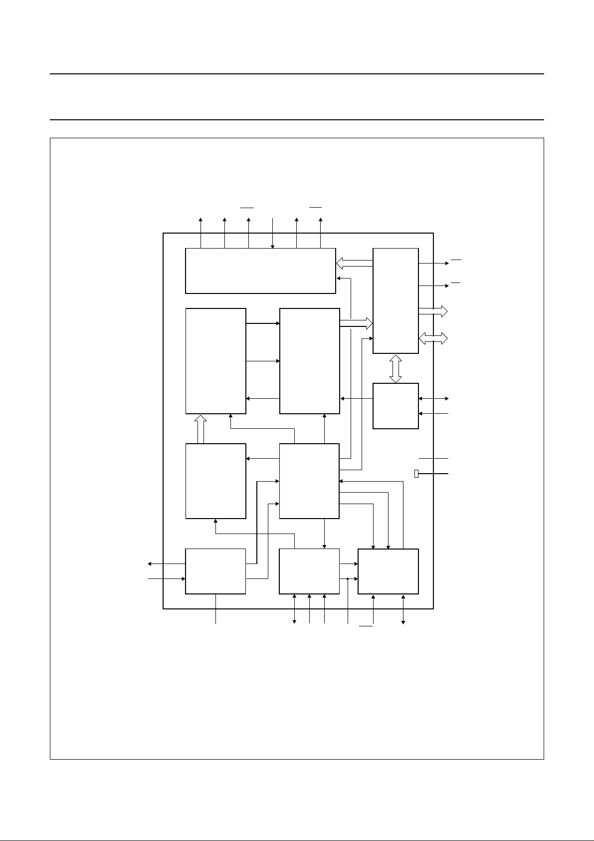
Fig.1 Block diagram for SOT240 (DIL48) package.
January 1993 3
INPUT
CLAMP
AND SYNC
DISPLAY
CLOCK
PHASE
LOCKED
LOOP
VCR / FFB
MLA840

Philips Semiconductors Product specification
Integrated VIP and Teletext (IVT1.0) SAA5246A
PINNING
SYMBOL
DESCRIPTION
SOT240 SOT319
OSCOUT 2 27 27 MHz crystal oscillator output
OSCIN 3 28 27 MHz crystal oscillator input
OSCGND 4 29 0 V crystal oscillator ground
PIN
V
SS
5, 14, 25 26, 30, 31,
0 V ground
43, 58
BLACK 7 35 video black level storage pin, connected to ground via a 100 nF capacitor
CVBS 8 36 composite video input pin. A positive-going 1 V (peak-to-peak) input is
required, connected via a 100 nF capacitor
IREF 9 37 reference current input pin, connected to ground via a 27 kΩ resistor
V
DD
1, 6, 10 25, 32, 38 +5 V positive supply
POL 11 39 STTV/LFB/FFB polarity selection pin
STTV/LFB 12 40 sync to TV output pin/line flyback input pin. Function controlled by an
internal register bit (scan sync mode)
VCR/FFB 13 42 PLL time constant switch/field input pin. Function controlled by an internal
register bit (scan sync mode)
R 15 44 dot rate character output of the RED colour information
G 16 45 dot rate character output of the GREEN colour information
B 17 47 dot rate character output of the BLUE colour information
RGBREF 18 48 input DC voltage to define the output high level on the RGB pins
BLAN 19 52 dot rate fast blanking output
COR 20 53 programmable output to provide contrast reduction of the TV picture for
mixed text and picture displays or when viewing newsflash/subtitle pages.
Open-drain output
ODD/EVEN 21 54 a 25 Hz output synchronized to the input CVBS field sync pulses to make a
non-interlaced display by adjustment of the vertical deflection currents.
Y 22 55 dot rate character output of teletext foreground colour information.
Open-drain output
2
SCL 23 56 serial clock input for I
C-bus. It can still be driven HIGH during power-down
of the device
SDA 24 57 serial data port for the I
2
C-bus. Open drain output. It can still be driven
HIGH during power-down of the device
D0-D5 26-31 60-64, 3 data ports for the page SRAM
n.c. − 1, 2, 10, 11,
not connected
15, 18, 33,
34, 41, 46,
49 - 51, 59
D6-D7 32, 33 4, 5 data ports for the page SRAM
January 1993 4

Philips Semiconductors Product specification
Integrated VIP and Teletext (IVT1.0) SAA5246A
SYMBOL
SOT240 SOT319
A0-A12 34-46 6-9, 12-14,
OE 47 23 output enable for the page SRAM
WE 48 24 write enable for the page SRAM
PIN
DESCRIPTION
address output for the page SRAM
16, 17,
19-22
January 1993 5
Philips Semiconductors Product specification
Integrated VIP and Teletext (IVT1.0) SAA5246A
handbook, halfpage
OSCOUT
OSCGND
STTV / LFB
VCR / FFB
V
DD
OSCIN
V
SS
V
DD
BLACK
CVBS
IREF
V
DD
POL
V
SS
1
2
3
4
5
6
7
8
9
10
11
12
SAA5246A
13
14
R
15
G
16
B
17
48
WE
47
OE
46
A12
45
A11
44
A10
43
A9
42
A8
41
A7
A6
40
A5
39
38
A4
A3
37
36
A2
35
A1
34
A0
33
D7
32
D6
RGBREF
ODD / EVEN
BLAN
COR
SCL
SDA
18
19
20
21
22
Y
23
24
MLA841
31
D5
30
D4
29
D3
28
D2
27
D1
26
D0
V
25
SS
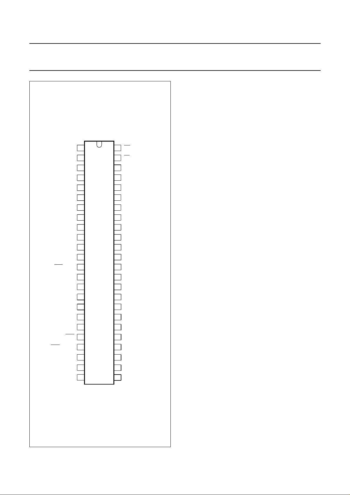
Fig.2 Pin configuration; SOT240 (DIL48).
January 1993 6
Philips Semiconductors Product specification
Integrated VIP and Teletext (IVT1.0) SAA5246A
handbook, full pagewidth
index
corner
n.c.
n.c.
D5
D6
D7
A0
A1
A2
A3
n.c.
n.c.
A4
A5
A6
n.c.
A7
A8
D4
D3
D2
D1
64
63
62
61
1
2
3
4
5
6
7
8
9
10
11
12
13
14
15
16
17
D0
60
SAA5246A
n.c.
59
SCL
56
Y
55
ODD / EVEN
54
SDA
V
58
57
SS
COR
53
BLAN
52
51
50
49
48
47
46
45
44
43
42
41
40
39
38
37
36
35
n.c.
RGBREF
B
n.c.
G
R
V
SS
VCR / FFB
n.c.
STTV / LFB
POL
V
DD
IREF
CVBS
BLACK
18
n.c.
19
A9
20
21
A10
A11
22
A12
23
OE
24
WE
25
DD
V
V
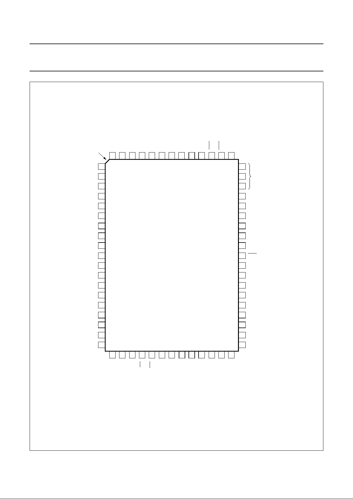
Fig.3 Pin configuration; SOT319 (QFP64).
January 1993 7
26
SS
27
28
OSCIN
OSCOUT
29
30
SS
V
OSCGND
34
n.c.
33
n.c.
31
32
SS
DD
V
V
MLA843

Philips Semiconductors Product specification
Integrated VIP and Teletext (IVT1.0) SAA5246A
LIMITING VALUES
In accordance with Absolute Maximum System (IEC 134)
SYMBOL PARAMETER MIN. MAX. UNIT
V
DD
V
I
V
O
I
O
I
IOK
T
amb
T
stg
V
stat
Note to the Limiting values
1. Electrostatic handling is equivalent to discharging a 100 pF capacitor through a 1.5 kΩ series resistor with a 15 ns
rise time.
supply voltage (all supplies) −0.3 6.5 V
input voltage (any input) −0.3 VDD+0.5 V
output voltage (any output) −0.3 VDD+0.5 V
output current (each output) −±10 mA
DC input or output diode current −±20 mA
operating ambient temperature −20 +70 °C
storage temperature −55 +125 °C
electrostatic handling (see note 1) −2000 +2000 V
Failure Rate
The failure rate at T
= 55 °C will be a maximum of 1000 FITS (1 FIT = 1 × 10⁻⁹ failures per hour).
amb
January 1993 8
Philips Semiconductors Product specification
Integrated VIP and Teletext (IVT1.0) SAA5246A
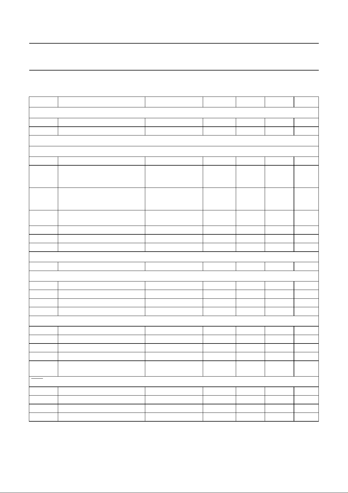
CHARACTERISTICS
= 5 V ± 10%; T
V
DD
SYMBOL PARAMETER CONDITIONS MIN. TYP. MAX. UNIT
Supplies
V
DD
I
DD
supply voltage range 4.5 5.0 5.5 V
total supply current − 64 128 mA
Inputs
CVBS
V
t
syn
syn
sync amplitude 0.1 0.3 0.6 V
delay from CVBS to TCS output
from STTV buffer (nominal video,
average of leading/trailing edge)
t
syd
change in sync delay between all
black and all white video input at
nominal levels
V
vid(p-p)
video input amplitude
(peak-to-peak)
display PLL catching range ±7 −−%
Z
src
C
I
source impedance −−250 Ω
input capacitance −−10 pF
IREF
R
g
resistor to ground − 27 − kΩ
POL
V
IL
V
IH
I
LI
C
I
LOW level input voltage −0.3 − +0.8 V
HIGH level input voltage 2.0 − VDD+0.5 V
input leakage current VI = 0 to V
input capacitance −−10 pF
LFB
V
V
I
I
t
IL
IH
LI
I
LFB
LOW level input voltage −0.3 − +0.8 V
HIGH level input voltage 2.0 − VDD+0.5 V
input leakage current VI = 0 to V
input current note 1 −1 − +1 mA
delay between LFB front edge
and input video line sync
VCR/FFB
V
IL
V
IH
I
LI
I
I
LOW level input voltage −0.3 − +0.8 V
HIGH level input voltage 2.0 − VDD+0.5 V
input leakage current VI = 0 to V
input current note 1 −1 − +1 mA
= −20 to +70 °C, unless otherwise specified
amb
DD
DD
DD
−150 0 +150 ns
0 − 25 ns
0.7 1.0 1.4 V
−10 − +10 µA
−10 − +10 µA
− 250 − ns
−10 − +10 µA
January 1993 9
Philips Semiconductors Product specification
Integrated VIP and Teletext (IVT1.0) SAA5246A
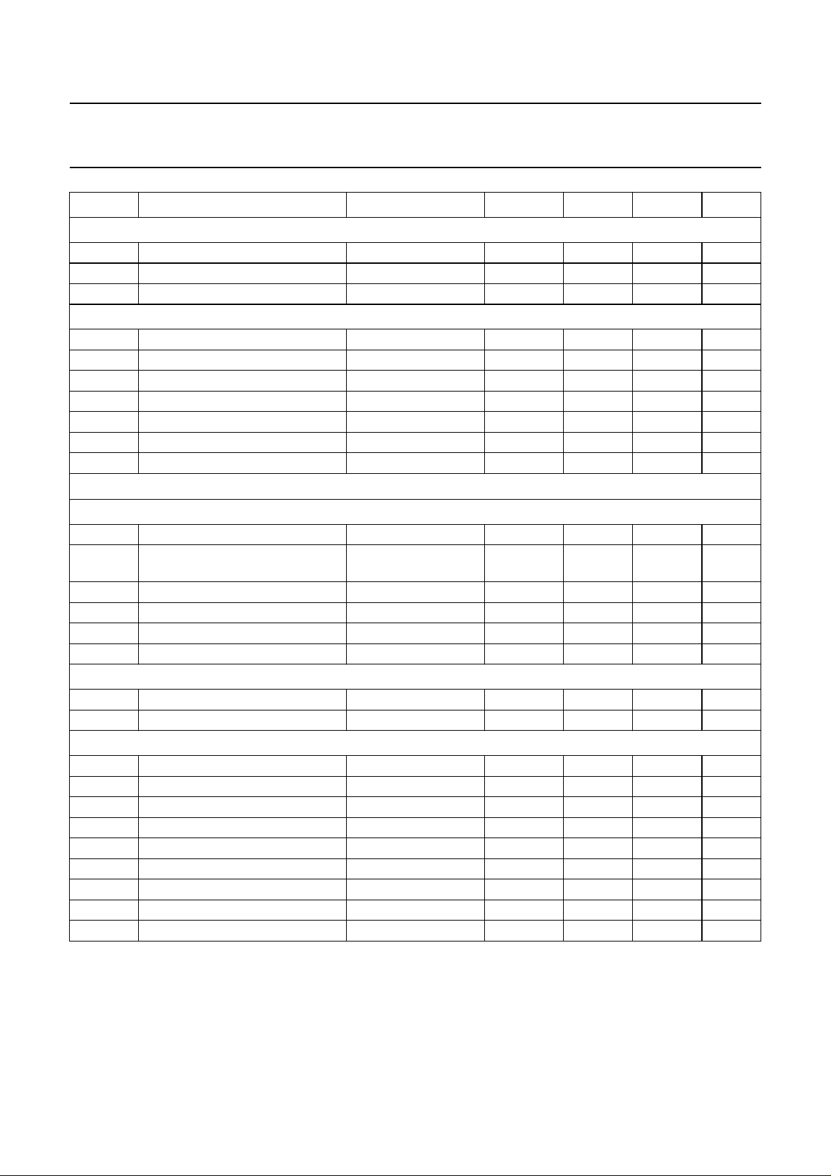
SYMBOL PARAMETER CONDITIONS MIN. TYP. MAX. UNIT
RGBREF
V
IL
I
LI
I
DC
SCL
V
IL
V
IH
I
LI
f
SCL
t
r
t
f
C
I
Inputs/outputs
LOW level input voltage −0.3 − VDD+0.5 V
input leakage current VI = 0 to V
DD
−10 − +10 µA
DC current −−10 mA
LOW level input voltage −0.3 − +1.5 V
HIGH level input voltage 3.0 − VDD+0.5 V
input leakage current VI = 0 to V
DD
−10 − +10 µA
clock frequency 0 − 100 kHz
input rise time 10% to 90% −−2µs
input fall time 90% to 10% −−2µs
input capacitance −−10 pF
RYSTAL OSCILLATOR (OSCIN; OSCOUT)
C
f
XTAL
V
OSC
crystal frequency − 27 − MHz
oscillation amplitude
(peak-to-peak value)
G
v
G
m
C
I
C
FB
small signal voltage gain − 1 − V/V
mutual conductance 5 −−mA/V
input capacitance −−10 pF
feedback capacitance − 1 − pF
BLACK
C
blk
I
LI
storage capacitor to ground − 100 − nF
input leakage current VI = 0 to V
SDA
V
IL
V
IH
I
LI
C
I
t
r
t
f
V
OL
t
f
C
L
LOW level input voltage −0.3 − +1.5 V
HIGH level input voltage 3.0 − VDD+0.5 V
input leakage current VI = 0 to V
input capacitance −−10 pF
input rise time 10% to 90% −−2µs
input fall time 90% to 10% −−2µs
LOW level output voltage IOL = 3 mA 0 − 0.5 V
output fall time 3 V to 1 V −−200 ns
load capacitance −−400 pF
DD
DD
− 1.5 − V
−10 − +10 µA
−10 − +10 µA
January 1993 10
Philips Semiconductors Product specification
Integrated VIP and Teletext (IVT1.0) SAA5246A
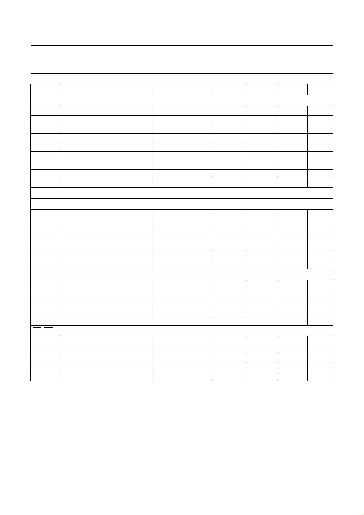
SYMBOL PARAMETER CONDITIONS MIN. TYP. MAX. UNIT
D0 TO D7
V
IL
V
IH
I
LI
C
I
V
OL
V
OH
t
r
t
f
C
L
Outputs
STTV
G
stt
V
tcs
V
DCs
I
O
C
L
A0 TO A12 ADDRESS OUTPUT TO MEMORY
V
OL
V
OH
C
L
t
r
t
f
OE, WE
V
OL
V
OH
C
L
t
r
t
f
LOW level input voltage −0.3 − +0.8 V
HIGH level input voltage 2.0 − VDD+0.5 V
input leakage current −10 − +10 µA
input capacitance −−10 pF
LOW level output voltage IOL = +1.6 mA 0 − 0.4 V
HIGH level output voltage IOH = −0.2 mA 2.4 − V
DD
V
output rise time 0.6 V to 2.2 V −−50 ns
output fall time 2.2 V to 0.6 V −−50 ns
load capacitance −−120 pF
gain of STTV relative to video
0.9 1.0 1.1
input
TCS amplitude 0.2 0.3 0.45 V
DC shift between TCS output and
−−0.15 V
nominal video output
output drive current −−3.0 mA
load capacitance −−100 pF
LOW level output voltage IOL = +1.6 mA 0 − 0.4 V
HIGH level output voltage IOH = −0.2 mA 2.4 − V
DD
V
load capacitance −−120 pF
output rise time 0.6 V to 2.2 V −−50 ns
output fall time 2.2 V to 0.6 V −−50 ns
LOW level output voltage IOL = +1.6 mA 0 − 0.4 V
HIGH level output voltage IOH = −0.2 mA 2.4 − V
DD
V
load capacitance −−120 pF
output rise time 0.6 V to 2.2 V −−50 ns
output fall time 2.2 V to 0.6 V −−50 ns
January 1993 11
Philips Semiconductors Product specification
Integrated VIP and Teletext (IVT1.0) SAA5246A
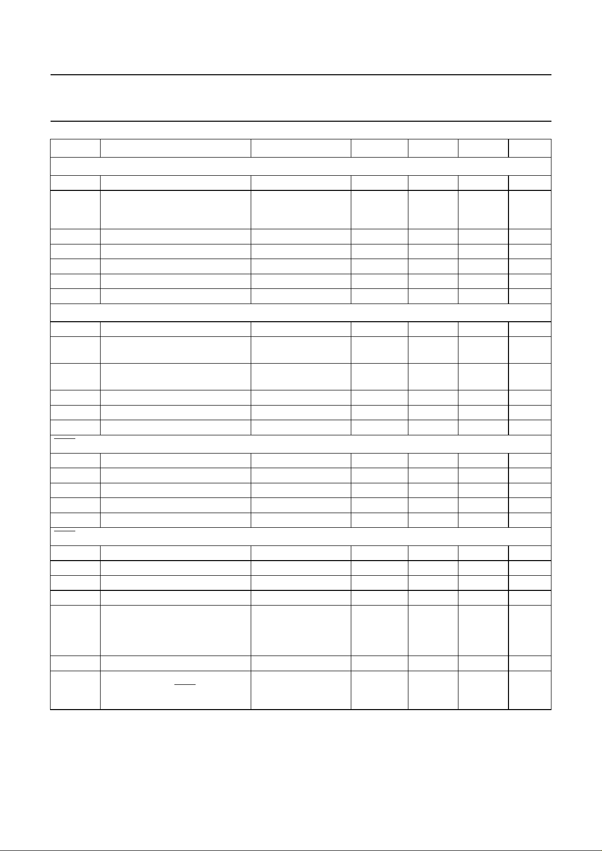
SYMBOL PARAMETER CONDITIONS MIN. TYP. MAX. UNIT
R, G AND B
V
OL
V
OH
I
DC
| output impedance −−200 Ω
|Z
o
C
L
t
r
t
f
BLAN
V
OL
V
OH
V
OH
C
L
t
r
t
f
ODD/EVEN
V
OL
V
OH
C
L
t
r
t
f
COR AND Y(OPEN DRAIN)
V
OH
V
OL
V
OL
C
L
t
f
I
LO
T
SK
LOW level output voltage IOL = 2 mA 0 − 0.2 V
HIGH level output voltage IOH = −1.6 mA;
RGBREF ≤
RGBREF
−0.25 V
RGBREF RGBREF
+0.25 V
V
VDD−2 V; note 2
DC current −−−3.3 mA
load capacitance −−50 pF
output rise time 10% to 90% −−20 ns
output fall time 90% to 10% −−20 ns
LOW level output voltage IOL = 0.2 mA 0 − 0.4 V
HIGH level output voltage IOH = −0.2 mA;
1.1 −−V
VDD = 4.5 V; note 2
HIGH level output voltage IOH = 0 mA;
−−2.8 V
VDD = 5.5 V; note 2
load capacitance −−50 pF
output rise time 10% to 90% −−20 ns
output fall time 90% to 10% −−20 ns
LOW level output voltage IOL = +1.6 mA 0 − 0.4 V
HIGH level output voltage IOH = −1.6 mA VDD−0.4 − V
DD
V
load capacitance −−120 pF
output rise time 0.6 to 2.2 V −−50 ns
output fall time 2.2 to 0.6 V −−50 ns
pull-up voltage at pin −−VDDV
LOW level output voltage IOL = +2 mA 0 − 0.4 V
LOW level output voltage IOL = +5 mA 0 − 1.0 V
load capacitance −−25 pF
output fall time load resistor of 1.2 kΩ
−−50 ns
to VDD; measured
between VDD−0.5
and 1.5 V
output leakage current VI = 0 to V
skew delay between display
DD
−10 − +10 µA
−−20 ns
outputs R, G, B, COR, Y and
BLAN
January 1993 12

Philips Semiconductors Product specification
Integrated VIP and Teletext (IVT1.0) SAA5246A
SYMBOL PARAMETER CONDITIONS MIN. TYP. MAX. UNIT
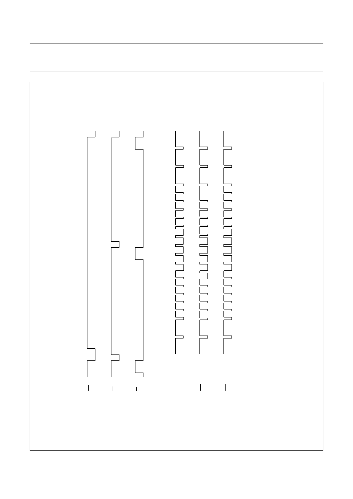
Timing
MEMORY INTERFACE
t
CY
t
OE
t
ADDR
t
rOEW
t
wOEW
t
ACC
t
DH
t
WEW
t
DS
t
DHWE
t
WR
t
DE
I2C-BUS
t
LOW
t
HIGH
t
SU;DAT
t
HD;DAT
t
SU;STO
t
BUF
t
HD;STA
t
SU;STA
cycle time − 500 − ns
address change to OE LOW 55 −−ns
address active time 450 500 − ns
OE pulse width read 295 −−ns
OE pulse width write 100 −−ns
access time from address data
−−150 ns
valid
data hold time from OE HIGH or
0 − 150 ns
address change
WE pulse width 100 −−ns
data set-up time to WE HIGH 60 −−ns
data hold time from WE HIGH 20 −−ns
write recovery time 20 −−ns
data enable from WE LOW 60 −−ns
clock LOW period 4 −−µs
clock HIGH period 4 −−µs
data set-up time 250 −−ns
data hold time 170 −−ns
set-up time from clock HIGH to
4 −−µs
STOP
START set-up time following a
4 −−µs
STOP
START hold time 4 −−µs
START set-up time following
4 −−µs
clock LOW-to-HIGH transition
Notes to the characteristics
1. This current is the maximum allowed into the inputs when line and field flyback signals are connected to these inputs.
Series current limiting resistors must be used to limit the input currents to ± 1 mA.
2. Can be pulled higher by external pull-up resistor, (maximum leakage current ≈ 200 µA).
January 1993 13
Philips Semiconductors Product specification
Integrated VIP and Teletext (IVT1.0) SAA5246A
64 µs
64 µs
32 34.33
64 µs
59.33
27.33 32
1 2 3456 7
625
(312)
624
(311)
623
(310)
MLA037 - 2
handbook, full pagewidth
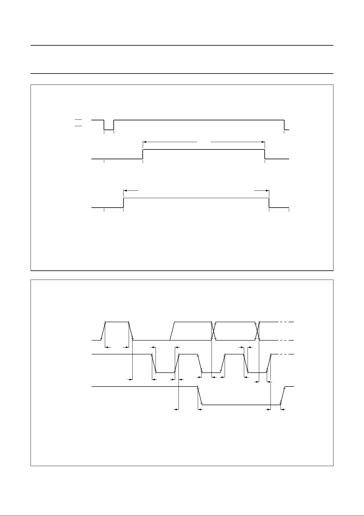
Fig.4 Composite sync waveforms.
622
(309)
[1]
621
(308)
0 4.66
0 2.33
LSP
(Line Sync Pulse)
0
EP
(Equalizing Pulse)
BP
(Broad Pulse)
January 1993 14
309 310 311 312 313 314 (1) 315 (2) 316 (3) 317 (4) 318 (5) 319 (6) 320 (7)
TCS interlaced
308 309 310 311 312 1 2 3 4 5 6 7
TCS interlaced
[2]
TCS non-interlaced
TCS is available on STTV/LFB pin.
[1] LSP, EP andBP are combined to give TCS as shown below. All timings measured from falling edge of LSP.
[2] Line numbers placed in the middle of the line. Equivalent count numbers in brackets.
Philips Semiconductors Product specification
Integrated VIP and Teletext (IVT1.0) SAA5246A
handbook, full pagewidth
LSP
(TCS)
0 4.66
R, G, B, Y
(1)
0
R, G, B, Y
(1)
0
(1) also BLAN in character and box blanking
Fig.5 Display output timing (a) line rate (b) field rate.
40 µs
display period
16.67
lines 42 to 291 inclusive (and 355 to 604 inclusive interlaced)
41
(a) LINE RATE
display period
(b) FIELD RATE
56.67 µs
64 µs
291
line numbers
MLA662 - 1
312
handbook, full pagewidth
SDA
t
LOW
t
SCL
SDA
MBC764
t
BUF
t
HD;STA
Fig.6 I2C-bus timing.
January 1993 15
t
r
SU;STA
t
HD;DAT
t
t
HIGH
f
t
SU;DAT
t
SU;STO
 Loading...