
INTEGRATED CIRCUITS
DATA SH EET
SAA4996H
Motion Adaptive Colour Plus And
Control IC (MACPACIC) for
PALplus
Preliminary specification
File under Integrated Circuits, IC02
1996 Oct 28

Philips Semiconductors Preliminary specification
Motion Adaptive Colour Plus And
Control IC (MACPACIC) for PALplus
CONTENTS
1 FEATURES
2 GENERAL DESCRIPTION
3 QUICK REFERENCE DATA
4 ORDERING INFORMATION
5 BLOCK DIAGRAMS
6 PINNING
7 FUNCTIONAL DESCRIPTION
7.1 Introduction
7.1.1 Data processing
7.1.2 Control
7.2 General requirements
7.3 Hardware configurations and delays
7.3.1 Full PALplus module (see Fig.5)
7.3.2 Stand-alone MACPACIC (see Fig.6)
7.4 Analog processing in front of the PALplus
module
7.5 Block diagram
7.6 Luminance and helper processing
7.6.1 Input range
7.7 Luminance processing
7.7.1 Luminance helper processing
7.8 Output signals
7.9 Measurements
7.9.1 Line 22 offset reference measurement
7.9.2 Line 23 and 623 amplitude reference
measurement
7.9.3 Noise measurement in line 23 and 623
7.10 Automatic gain and offset control
7.10.1 SNERT control bits influencing the AGC and
AOC
7.10.2 Gain control
7.10.3 Offset control
7.10.4 Helper amplitude and bandwidth control
7.11 Output range
7.12 Chrominance
7.12.1 Input range
7.12.2 Chrominance processing
7.12.3 Output signals
7.12.4 Output range
7.13 Chrominance motion detection
7.14 Intelligent residual cross-luminance reduction
(IRXR)
7.15 Control
7.15.1 Input reference signals
7.15.2 Functional description
7.15.3 SNERT interface (see application note
AN95XXX)
SAA4996H
8 TEST
8.1 Boundary scan test
8.1.1 Identification codes
9 DC CHARACTERISTICS
10 AC CHARACTERISTICS
10.1 Clock buffers
11 LIST OF ABBREVIATIONS
12 PACKAGE OUTLINE
13 SOLDERING
13.1 Introduction
13.2 Reflow soldering
13.3 Wave soldering
13.4 Repairing soldered joints
14 DEFINITIONS
15 LIFE SUPPORT APPLICATIONS
1996 Oct 28 2

Philips Semiconductors Preliminary specification
Motion Adaptive Colour Plus And Control
SAA4996H
IC (MACPACIC) for PALplus
1 FEATURES
• Motion adaptive colour plus decoding
• Helper AGC/AOC
• Helper decompanding
• Memory controlling
• VERIC controlling.
2 GENERAL DESCRIPTION
The SAA4996H (MACPACIC) performs the Motion
Adaptive Colour Plus (MACP) processing which is a
dedicated field comb filter technique exploited for the
PALplus system.
3 QUICK REFERENCE DATA
SYMBOL PARAMETER MIN. MAX. UNIT
V
DD
T
amb
T
die
digital supply voltage 4.75 5.25 V
operating ambient temperature 0 +70 °C
die temperature − +125 °C
The integrated circuit is especially designed to be used in
conjunction with the SAA4997H Vertical Reconstruction IC
(VERIC) to decode the transmitted PALplus video signals
in PALplus colour TV receivers.
In addition, a hardware configuration ‘stand-alone
MACPACIC’ with only two field memories (FM1 and FM4)
is also possible. In this condition no helper lines are
processed and no vertical reconstruction is applied.
This configuration enables the Motion Adaptive Colour
Plus processing to be performed in non PALplus receivers.
4 ORDERING INFORMATION
TYPE
NUMBER
SAA4996H QFP100
NAME DESCRIPTION VERSION
PACKAGE
plastic quad flat package; 100 leads (lead length 1.95 mm);
body 14 × 20 × 2.7 mm; high stand-off height
SOT317-1
1996 Oct 28 3
Philips Semiconductors Preliminary specification
Motion Adaptive Colour Plus And Control
IC (MACPACIC) for PALplus
5 BLOCK DIAGRAMS
handbook, full pagewidth
Y_ADC
Y_FM1
U_ADC
V_ADC
U_FM1
V_FM1
17 to 24
1 to 8
15, 16,
13, 14
11, 12,
9, 10
8
8
4
CHROMINANCE
4
PROCESSING
UV_IFA
SAA4996H
LUMINANCE AND
HELPER PROCESSING
4
CS
YL
SAA4996H
60, 59,
57 to 52
8
37 to 44
8
45
61, 62,
63, 64
4
3
1
MUX
3
0
SEL
IVericN
46, 47,
48
3
91, 92,
4
89, 90
Y_MA
Y_TO_FM1
U_TO_FM1_0
U_MA, V_MA
WE_FM2 / U_TO_FM1_1
WE_FM3 / V_TO_FM1_1
RSTW_FM23 / V_TO_FM1_0
U_TO_FM4
V_TO_FM4
U_FM4
V_FM4
VA_FRONT
CLAMP
WE_FRONT
SNERT_DA
SNERT_CL
SNERT_RST
85, 86,
87, 88
81
29
36
82
83
84
4
VERIC_AV_N
CHROMINANCE
MOTION DETECTION
AND IRXR
control
SNERT INTERFACE
25, 49,
67, 73,
96
V
DD1
to V
V
SS1
DD5
26, 50,
66, 74,
CLK_16i
CLK_32i
97
to V
SS5
CLOCK
BUFFER
CLK_16
CLK_32
CONTROL
70332758 72 71 69
TDI
TMS
TCK
TEST
TRSTN
3
3
99
100
94
95
93
79
80
28
76
77
78
98, 75, 35
51, 31, 65
68
30,
32, 34
TEST1,2,3
RE_FM1
WE_FM1
RE_FM4
WE_FM4
RST_FM14
VA_AI
HREF_MA
WE_MA
EVEN_FIELD
FILM
INTPOL
CLK_16B1,2,3
CLK_32B1,2,3
TDO_MA
MHA133
1996 Oct 28 4
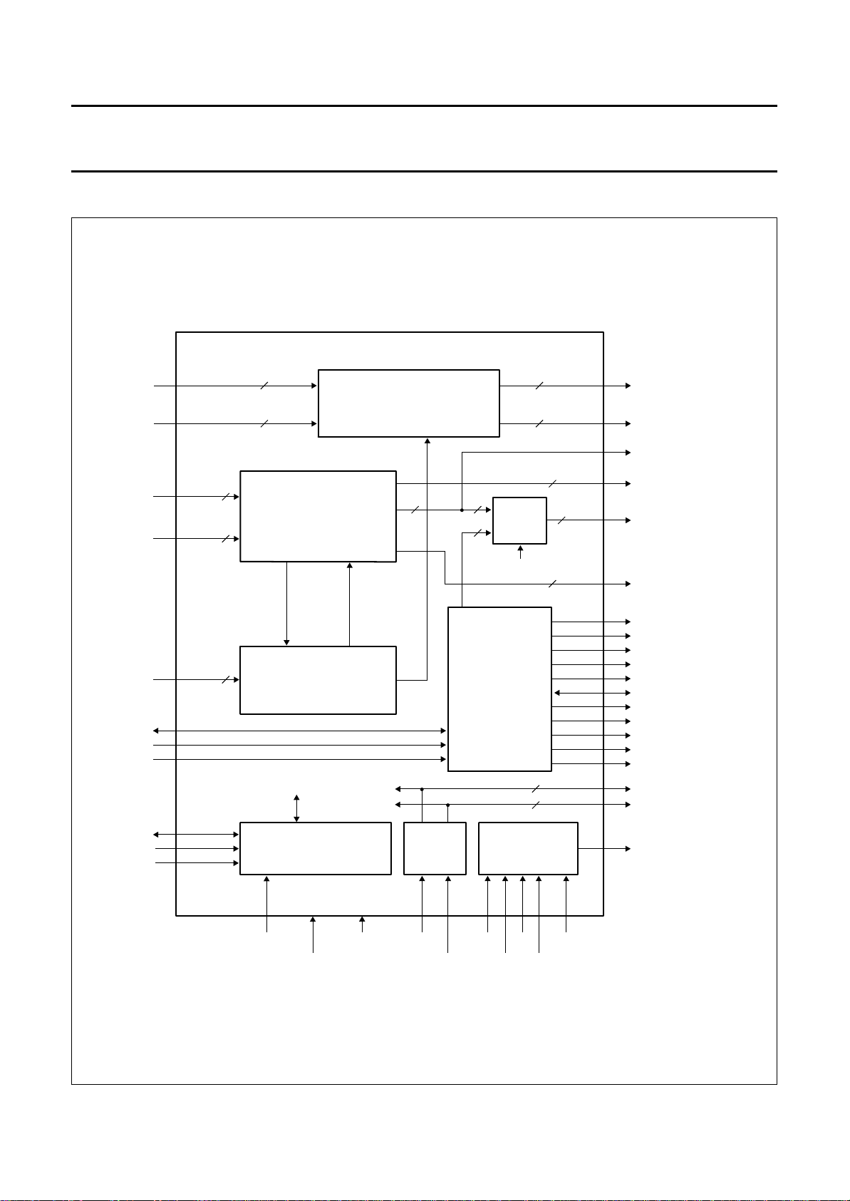
Fig.1 Block diagram.
Philips Semiconductors Preliminary specification
Motion Adaptive Colour Plus And Control
IC (MACPACIC) for PALplus
RST_FM14
RE_FM4
WE_FM1
H / V
VA_AI_DIFF
LOGIC
VA_RES
WE_FM4
IVericN
Mpip
CLK_16I
CLK_32I
WE_FM3
WE_FM2
16/32 MHz
H_RE / WE
PC2
PIXEL
PRE
RSTW_FM23
CONVERTER
6
PIXEL
DECODER
11
10 BIT
CLK
COUNTER 2
2 CLK_16
IVericN
LD = 2
line2_every_field
EVEN_FIELD
2
HlpM0,1
RE_FM1
V_RE / WE
LINE
DECODER
IVericN
6
HREF_MA
DELAY
CLAMP
WE_MA
FILM
2
HlpM0,1
VERIC
CONTROL
FilmOn
INTPOL
DECODER
Mpip
EVEN_FIELD
22Valid
SAA4996H
TDO_MA
TEST AND BST
MHA137
TEST3
TEST2
TRSTN TDI TMS TCK TEST1
VA_AI_DIFF
handbook, full pagewidth
VA_AI
Mpip
1
1
Mpip
0
VA_RES
VA_FR_DEL
0
CLK_16I
LC_ACQ
9
ACQ
LINE
PRE
DELAY
VA_FRONT
FIELD LENGTH
InvO/E
IVericN
9 BIT
COUNTER
CLK_16I
3
VaDel0-2
EVEN_FIELD
VA_AI
FIELD
DETECTION,
MEASUREMENT,
VA_RES
CLK_16I
CLP_DIFF
VA_FR_DEL
LD = 1
EN
CLP_DIFF
CLK_16I
PC2_PRE
(1/2 LINE)
VA_AI DELAY
PC1
LC_DSP
DSP
PRE
MUX2
0
1
1
VA_AI_DIFF
LINE
SEL
MUX1
CLK_16I
CLK_16I
CLK_16I
9
9 BIT
COUNTER
EN
Mpip
SEL
0
LD = 1
IVericN
PRE
CLK_16I
WE_MA
WE_MA
GENERATION
PC1
10
PIXEL
10 BIT
COUNTER 1
CLK_32I
CLOCK
BUFFER
WeShift16_0,1
WeStrtH,V
WeStpH,V
36
LD = 2
CLK
CLK_16I
line2_every_field
EnIRXR
MpipFilmOn InvO/EMacpOn MotVis0,1
2 32
HlpM0,1
Preset VaDel0-2
3
7
7
SNERT INTERFACE
5
40
64
Control 6:
Interlace,
EnPreEvFld,
PreEvFld
Control 5:
BOH0-2,
VAA0,1,
SEL_SD_YL0,1,
Control 4:
SelSdYl0,1,
NmYl0,1,
Rha/Rhb0-2
Control 3:
22/23/623Valid,
IMacpacicN,
IVericN
IrxrThr1-4,
FixHlpMain
HlpRedThr1-5,
MacpYhThr1-3
NAIRXR
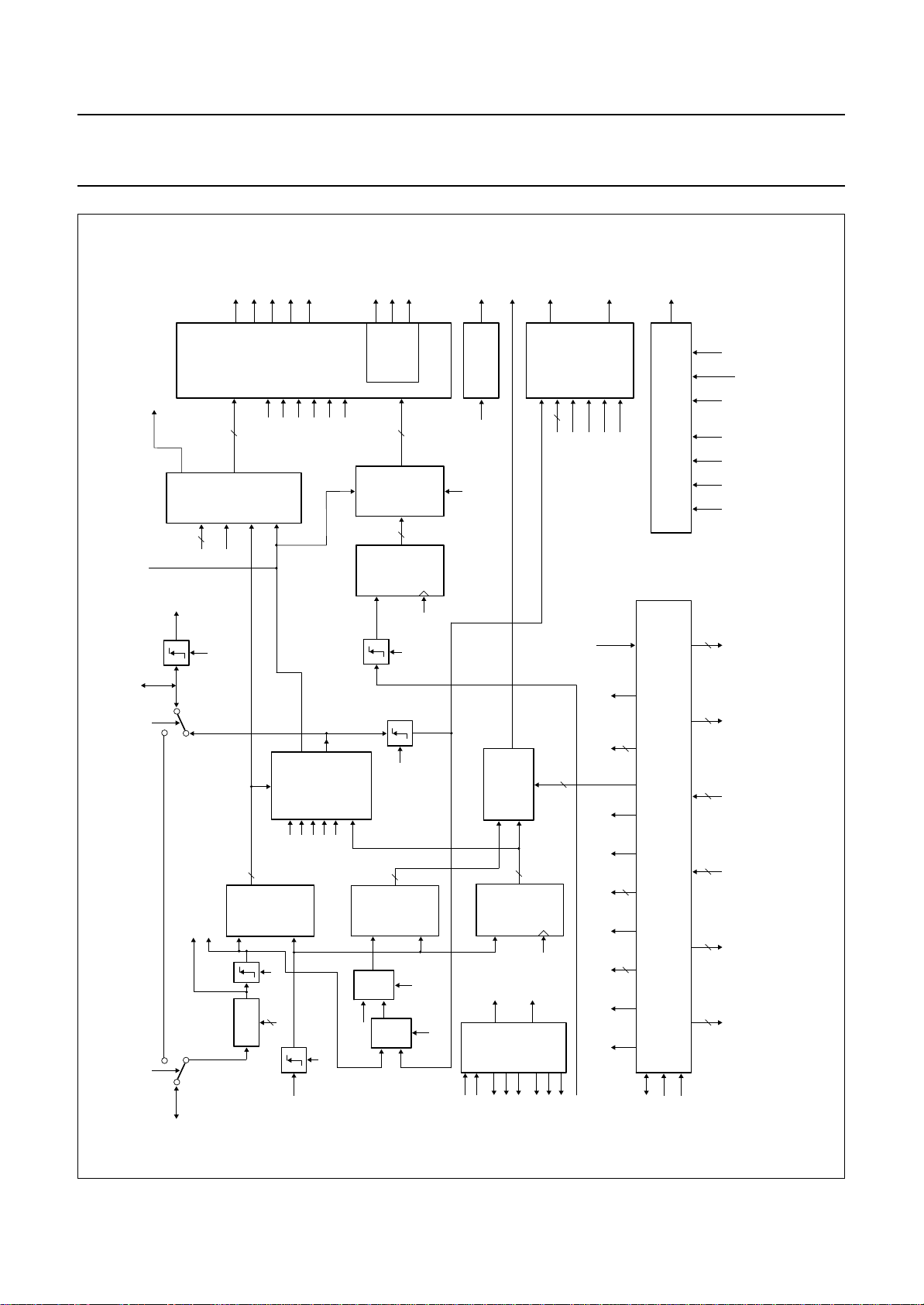
Fig.2 Block diagram of the control part.
VA_FRONT
1996 Oct 28 5
CLAMP
CLK_32
CLK_16
CLK_16B1
CLK_16B2
CLK_16B3
CLK_32B1
CLK_32B2
CLK_32B3
WE_FRONT
SNERT_CL
SNERT_DA
SNERT_RST
Philips Semiconductors Preliminary specification
Motion Adaptive Colour Plus And Control
IC (MACPACIC) for PALplus
Control 1
Control 2
Control 5
handbook, full pagewidth
Control 4
8
8
OUTPUT
REGISTER
2 ACQ DATA
8
FastTest_Del
SNERT_RST
adr_H65/H66
(bit D3)
FastTest
FAST TEST DELAY
8
8
DATA
INPUT
REGISTER
2 SYNCHRON
Control 2/2
Control 1/2
8
8
2 ACQ DATA
Control 1/1
Control 2/1
8
8
Line2_odd_every_field
INPUT
REGISTER
WeStrtH,
WeStpH
2 × 8
4 ACQ DATA
WeStrtH*,
WeStpH*
2 × 8
WeStrtV,
2 × 9
INPUT
REGISTER
2 × 9
WeStpV
WeStrtV*,
HlpRedThr1,2,3,4,5,
MacpYhThr1,2,3,
IrxrThr1,2,3,4,
FixHlpMain,
Control 5
14 × 8
1 SYNCHRON
SNERT_RST
WeStpV*
SAA4996H
Control 6
8
DATA
INPUT
REGISTER
Control 6/1
8
MHA138
Line2_every_field
DATA_OUT
to
21
adr_en_50h
ADDRESS
DECODER
ALE
DLE
REGISTER
SERIAL DATA I/O
DATA AND ADDRESS
SNERT_DA
21 ACTUAL
adr_en_68h
GENERATION
LATCH ENABLE
SNERT_CL
SNERT_RST
DATA
INPUT
REGISTER
DATA_IN
8
4 BIT COUNTER
SEND / RECEIVE
SNERT_RST
CONTROLLING
Interlace
Line2_odd_every_field
LINE 2
GENERATION
ENABLE SIGNAL
ODD / EVERY FIELD
EVEN_FIELD
Line2_every_field
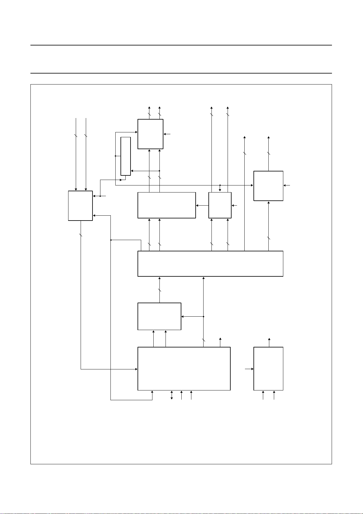
Fig.3 Block diagram of the SNERT interface.
1996 Oct 28 6

Philips Semiconductors Preliminary specification
Motion Adaptive Colour Plus And Control
SAA4996H
IC (MACPACIC) for PALplus
6 PINNING
SYMBOL PIN DESCRIPTION
Y_FM1_7 1 CVBS/helper/luminance input data bit 7 from FM1
Y_FM1_6 2 CVBS/helper/luminance input data bit 6 from FM1
Y_FM1_5 3 CVBS/helper/luminance input data bit 5 from FM1
Y_FM1_4 4 CVBS/helper/luminance input data bit 4 from FM1
Y_FM1_3 5 CVBS/helper/luminance input data bit 3 from FM1
Y_FM1_2 6 CVBS/helper/luminance input data bit 2 from FM1
Y_FM1_1 7 CVBS/helper/luminance input data bit 1 from FM1
Y_FM1_0 8 CVBS/helper/luminance input data bit 0 from FM1
V_FM1_0 9 chrominance input data bit 0 from FM1
V_FM1_1 10 chrominance input data bit 1 from FM1
U_FM1_0 11 chrominance input data bit 0 from FM1
U_FM1_1 12 chrominance input data bit 1 from FM1
V_ADC_0 13 chrominance input data bit 0 from ADC
V_ADC_1 14 chrominance input data bit 1 from ADC
U_ADC_0 15 chrominance input data bit 0 from ADC
U_ADC_1 16 chrominance input data bit 1 from ADC
Y_ADC_0 17 CVBS/helper/luminance data input bit 0 from ADC
Y_ADC_1 18 CVBS/helper/luminance data input bit 1 from ADC
Y_ADC_2 19 CVBS/helper/luminance data input bit 2 from ADC
Y_ADC_3 20 CVBS/helper/luminance data input bit 3 from ADC
Y_ADC_4 21 CVBS/helper/luminance data input bit 4 from ADC
Y_ADC_5 22 CVBS/helper/luminance data input bit 5 from ADC
Y_ADC_6 23 CVBS/helper/luminance data input bit 6 from ADC
Y_ADC_7 24 CVBS/helper/luminance data input bit 7 from ADC
V
DD1
V
SS1
CLK_16 27 16 MHz line-locked system clock input pulse
WE_MA 28 write enable output signal; defines active video data
CLAMP 29 horizontal reference input pulse
TEST1 30 test pin 1; must be LOW during normal operation
CLK_32B2 31 32 MHz line-locked clock output pulse
TEST2 32 test pin 2; must be LOW during normal operation
CLK_32 33 32 MHz line-locked system clock input pulse
TEST3 34 test pin 3; must be LOW during normal operation
CLK_16B3 35 16 MHz line-locked clock output pulse
WE_FRONT
Y_TO_FM1_0 37 CVBS/helper/luminance output data bit 0 to FM1; stand-alone MACPACIC
Y_TO_FM1_1 38 CVBS/helper/luminance output data bit 1 to FM1; stand-alone MACPACIC
Y_TO_FM1_2 39 CVBS/helper/luminance output data bit 2 to FM1; stand-alone MACPACIC
25 positive supply voltage 1
26 negative supply voltage 1
36
write enable input signal used as horizontal reference in the event of active
data
1996 Oct 28 7

Philips Semiconductors Preliminary specification
Motion Adaptive Colour Plus And Control
SAA4996H
IC (MACPACIC) for PALplus
SYMBOL PIN DESCRIPTION
Y_TO_FM1_3 40 CVBS/helper/luminance output data bit 3 to FM1; stand-alone MACPACIC
Y_TO_FM1_4 41 CVBS/helper/luminance output data bit 4 to FM1; stand-alone MACPACIC
Y_TO_FM1_5 42 CVBS/helper/luminance output data bit 5 to FM1; stand-alone MACPACIC
Y_TO_FM1_6 43 CVBS/helper/luminance output data bit 6 to FM1; stand-alone MACPACIC
Y_TO_FM1_7 44 CVBS/helper/luminance output data bit 7 to FM1; stand-alone MACPACIC
U_TO_FM1_0 45 chrominance output data to FM1; stand-alone MACPACIC
WE_FM2/U_TO_FM1_1 46 for full PALplus module; write enable for FM2 for stand-alone MACPACIC;
chrominance output to FM1
RSTW_FM23/V_TO_FM1_0 47 for full PALplus module; reset write for FM2/FM3 for stand-alone
MACPACIC; chrominance output to FM1
WE_FM3/V_TO_FM1_1 48 for full PALplus module; write enable for FM3 for stand-alone MACPACIC;
chrominance output to FM1
V
DD2
V
SS2
CLK_32B1 51 32 MHz line-locked clock output pulse
Y_MA_0 52 luminance output data bit 0 from MACPACIC
Y_MA_1 53 luminance output data bit 1 from MACPACIC
Y_MA_2 54 luminance output data bit 2 from MACPACIC
Y_MA_3 55 luminance output data bit 3 from MACPACIC
Y_MA_4 56 luminance output data bit 4 from MACPACIC
Y_MA_5 57 luminance output data bit 5 from MACPACIC
VERIC_AV_N 58 input configuration signal VERIC available (VERIC_AV_N = 0)
Y_MA_6 59 luminance output data bit 6 from MACPACIC
Y_MA_7 60 luminance output data bit 7 from MACPACIC
U_MA_0 61 chrominance output data bit 0 from MACPACIC
U_MA_1 62 chrominance output data bit 1 from MACPACIC
V_MA_0 63 chrominance output data bit 0 from MACPACIC
V_MA_1 64 chrominance output data bit 1 from MACPACIC
CLK_32B3 65 32 MHz line-locked clock output pulse
V
SS3
V
DD3
TDO_MA 68 boundary scan test: data output signal
TRSTN 69 boundary scan test: reset input signal
TDI 70 boundary scan test: data input signal
TMS 71 boundary scan test: multiplexer set input
TCK 72 boundary scan test: clock input signal
V
DD4
V
SS4
CLK_16B2 75 16 MHz line-locked clock output pulse
EVEN_FIELD 76 even field =0 = odd input field; even field =1 = even input field
49 positive supply voltage 2
50 negative supply voltage 2
66 negative supply voltage 3
67 positive supply voltage 3
73 positive supply voltage 4
74 negative supply voltage 4
1996 Oct 28 8

Philips Semiconductors Preliminary specification
Motion Adaptive Colour Plus And Control
SAA4996H
IC (MACPACIC) for PALplus
SYMBOL PIN DESCRIPTION
FILM 77 control output signal to select film or camera mode in VERIC;
FILM = 0: camera mode; FILM = 1: film mode; FILM = 1 and INTPOL = 0;
bypass mode for MultiPIP
INTPOL 78 INTPOL = 0 = vertical interpolation in the VERIC not active;
INTPOL = 1 = vertical interpolation in the VERIC active
VA_AI 79 vertical reference output pulse or vertical reference input pulse in MultiPIP
mode
HREF_MA 80 horizontal reference output pulse
VA_FRONT 81 vertical reference input pulse or vertical reference output pulse in MultiPIP
mode
SNERT_DA 82 Synchronous No parity Eight bit Reception and Transmission (SNERT)-bus
data
SNERT_CL 83 SNERT-bus clock
SNERT_RST 84 SNERT-bus reset
U_FM4_0 85 chrominance input data bit 0 from FM4
U_FM4_1 86 chrominance input data bit 1 from FM4
V_FM4_0 87 chrominance input data bit 0 from FM4
V_FM4_1 88 chrominance input data bit 1 from FM4
V_TO_FM4_1 89 chrominance output data bit 1 to FM4
V_TO_FM4_0 90 chrominance output data bit 0 to FM4
U_TO_FM4_1 91 chrominance output data bit 1 to FM4
U_TO_FM4_0 92 chrominance output data bit 0 to FM4
RST_FM14 93 reset read/write FM1 and FM4 output
RE_FM4 94 read enable FM4 output
WE_FM4 95 write enable FM4 output
V
DD5
V
SS5
CLK_16B1 98 16 MHz line-locked clock output pulse
RE_FM1 99 read enable FM1 output
WE_FM1 100 write enable FM1 output
96 positive supply voltage 5
97 negative supply voltage 5
1996 Oct 28 9
Philips Semiconductors Preliminary specification
Motion Adaptive Colour Plus And Control
IC (MACPACIC) for PALplus
handbook, full pagewidth
Y_FM1_7
Y_FM1_6
Y_FM1_5
Y_FM1_4
Y_FM1_3
Y_FM1_2
Y_FM1_1
Y_FM1_0
V_FM1_0
V_FM1_1
U_FM1_0
U_FM1_1
V_ADC_0
V_ADC_1
U_ADC_0
U_ADC_1
Y_ADC_0
Y_ADC_1
Y_ADC_2
Y_ADC_3
Y_ADC_4
Y_ADC_5
Y_ADC_6
Y_ADC_7
V
DD1
V
SS1
CLK_16
WE_MA
CLAMP
TEST1
SS5VDD5
WE_FM4
V
CLK_16B1
RE_FM1
WE_FM1
99989796959493929190898887868584838281
100
1
2
3
4
5
6
7
8
9
10
11
12
13
14
15
16
17
18
19
20
21
22
23
24
25
26
27
28
29
RST_FM14
RE_FM4
U_TO_FM4_0
SAA4996H
V_TO_FM4_1
V_TO_FM4_0
U_TO_FM4_1
V_FM4_0
V_FM4_1
U_FM4_0
U_FM4_1
SNERT_DA
SNERT_CL
SNERT_RST
VA_FRONT
80
HREF_MA
79
VA_AI
78
INTPOL
77
FILM
76
EVEN_FIELD
75
CLK_16B2
74
V
73
V
72
TCK
71
TMS
70
TDI
69
TRSTN
68
TDO_MA
67
V
66
V
65
CLK_32B3
64
V_MA_1
63
V_MA_0
U_MA_1
62
61
U_MA_0
60
Y_MA_7
59
Y_MA_6
VERIC_AV_N
58
57
Y_MA_5
56
Y_MA_4
55
Y_MA_3
Y_MA_2
54
53
Y_MA_1
52
Y_MA_0
5130
CLK_32B1
SAA4996H
SS4
DD4
DD3
SS3
1996 Oct 28 10
31323334353637383940414243444546474849
TEST2
TEST3
CLK_32
CLK_32B2
CLK_16B3
WE_FRONT
Y_TO_FM1_0
Y_TO_FM1_1
Y_TO_FM1_2
Y_TO_FM1_3
Y_TO_FM1_4
Y_TO_FM1_5
Y_TO_FM1_6
Y_TO_FM1_7
U_TO_FM1_0
WE_FM2/U_TO_FM1_1
RSTW_FM23/V_TO_FM1_0
WE_FM3/V_TO_FM1_1
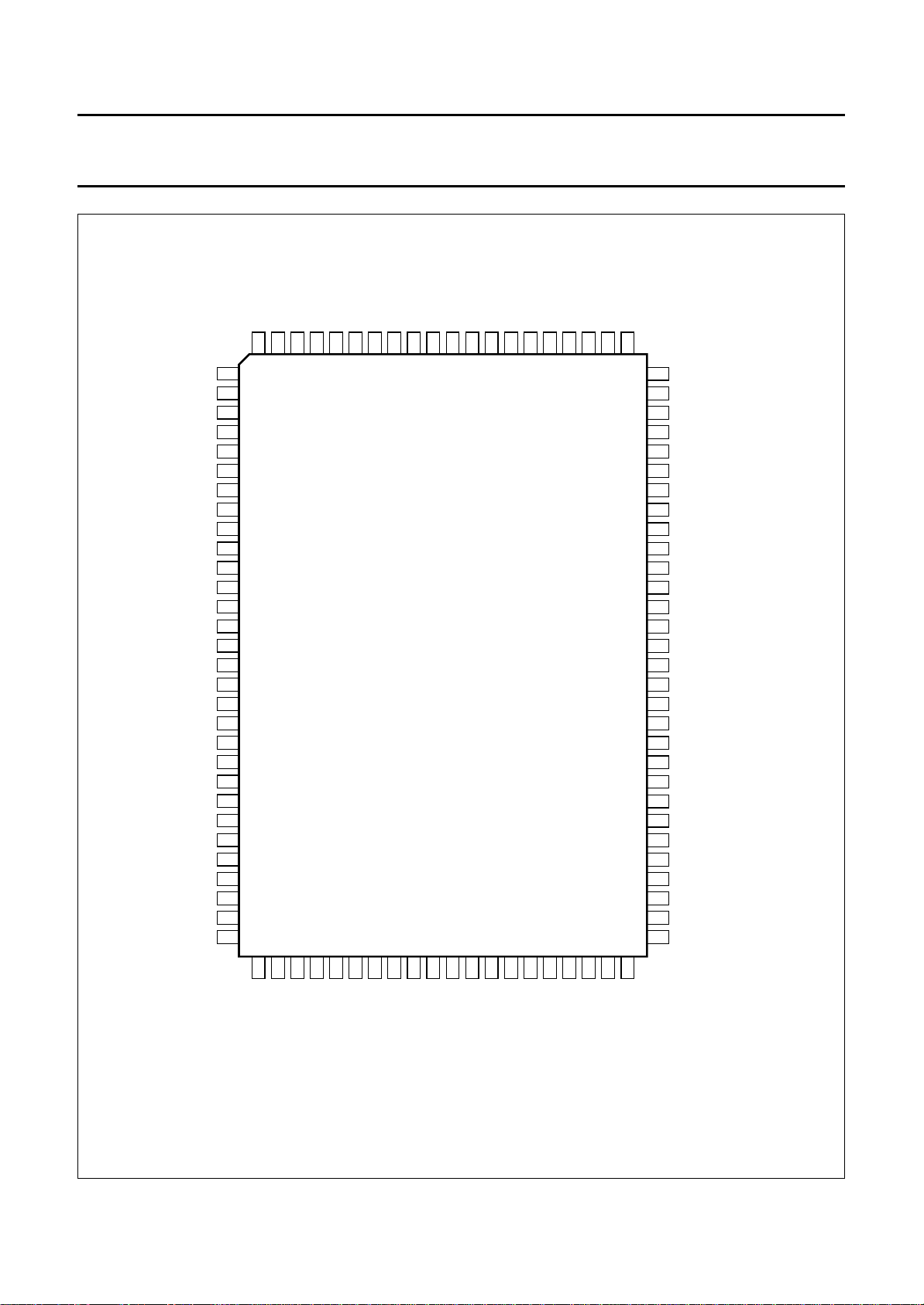
Fig.4 Pin configuration.
V
DD2
50
V
MHA134
SS2

Philips Semiconductors Preliminary specification
Motion Adaptive Colour Plus And Control
IC (MACPACIC) for PALplus
7 FUNCTIONAL DESCRIPTION
7.1 Introduction
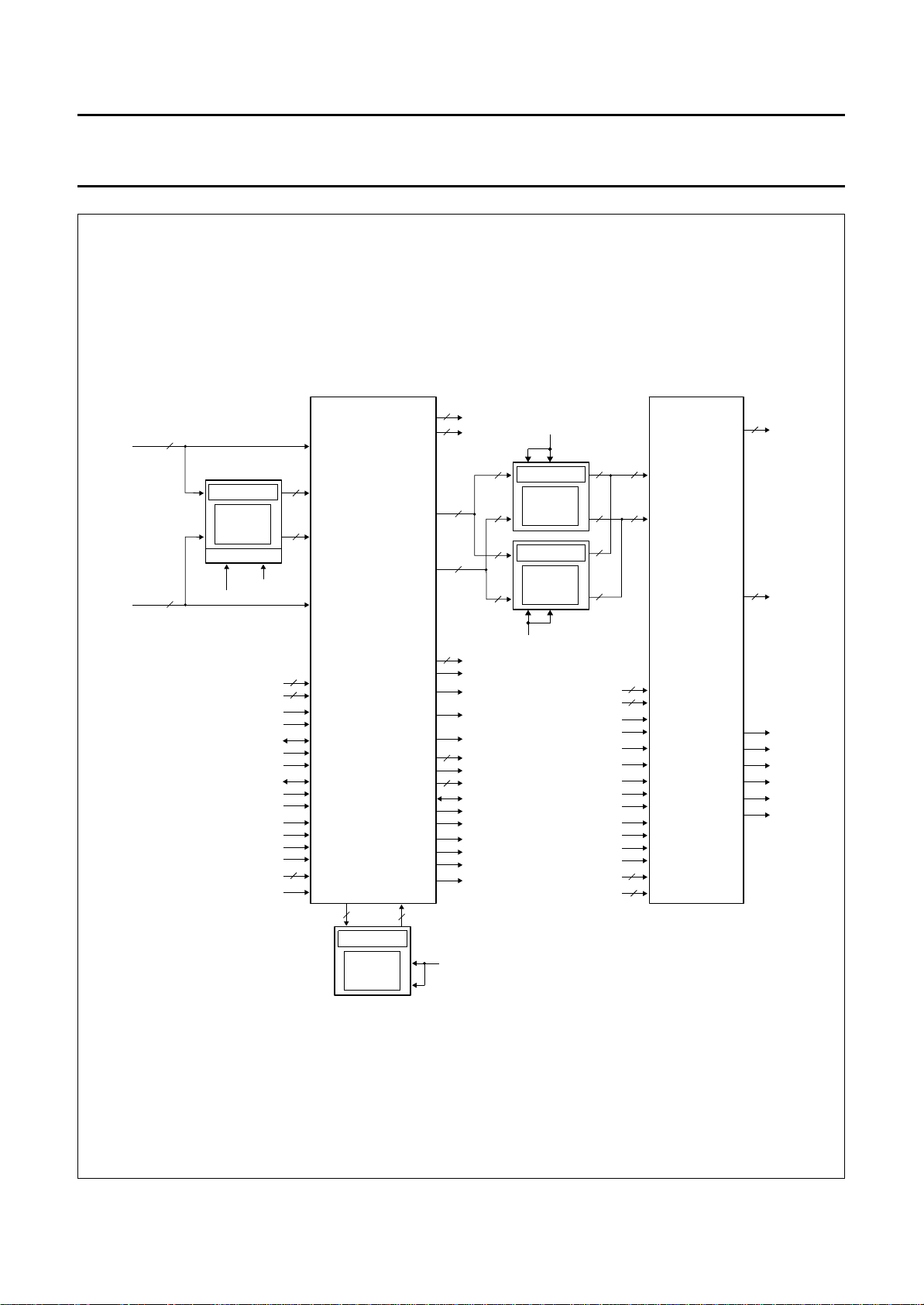
The MACPACIC is designed to be used in the PALplus
decoder module of a PALplus colour TV receiver. The full
PALplus decoder module consists of two special
integrated circuits and four field memories, as illustrated in
Fig.5.
The special ICs are as follows;
• Motion Adaptive Colour Plus And Control IC
(MACPACIC) for PALplus (SAA4996H)
• Vertical Reconstruction IC (VERIC) (SAA4997H).
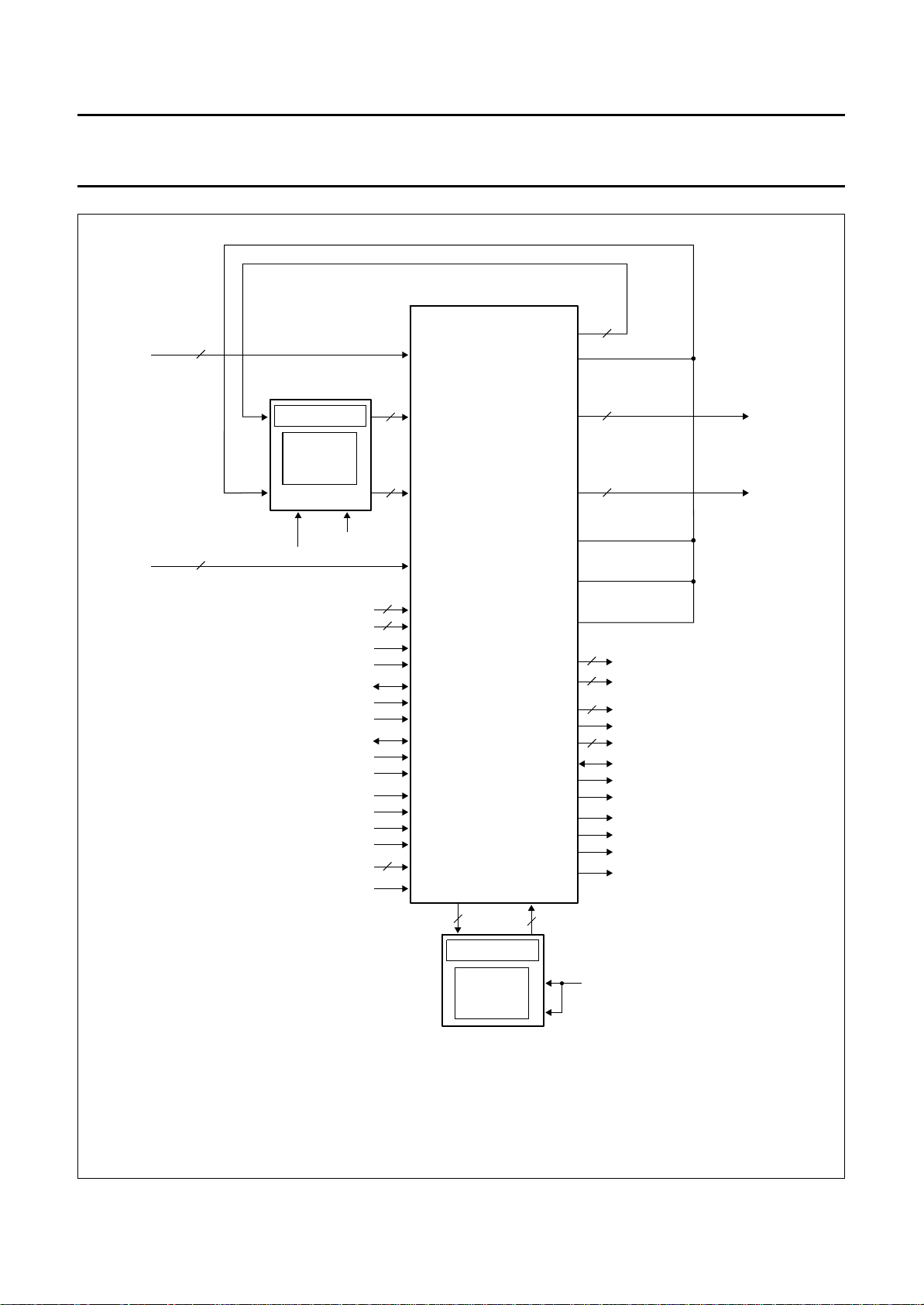
Besides the full PALplus module, a configuration for
stand-alone Motion Adaptive Colour Plus processing
(MACP) is also possible (see Fig.6). In this event only
MACPACIC with FM1 and FM4 are necessary.
This configuration enables the MACP processing in
non-PALplus receivers to be performed.
The PALplus module is designed to operate in conjunction
with a 100 Hz feature box. All special requirements such
as the delay of the PALplus module, bypass modes and
generation of the necessary control and clock signals will
be fulfilled.
7.1.1 D
The MACPACIC includes the decompanding functions for
the helper lines and the motion adaptive
luminance/chrominance separation in accordance with the
PALplus system description REV. 3.0 with some
modifications;
• The system operates at a clock frequency of 16 MHz
• The Y:U:V format is 4:1:1 instead of 4:2:2
• The filter DEC_MD_UV_LPF is not implemented
• If noisy helper signals are received, the helper
bandwidth and/or amplitude can be reduced
• Automatic gain control of the helper signal with respect
to the luminance signal.
The input signals are the BB(helper)/CVBS and
chrominance signals which are derived from the
analog-to-digital converter (ADC).
ATA PROCESSING
SAA4996H
7.1.2 C
Memory control, PALplus system controlling and clock
generation (from the incoming 16 MHz and 32 MHz
line-locked clocks) are implemented in the MACPACIC.
All clocks and control signals necessary for the PALplus
module (excluding read control of FM2/FM3) are
generated in the controller part. Inputs are reference
signals, clocks and control signals delivered by the
colour/helper decoder IC (TDA9144), and the 100 Hz
memory controller, i.e. ECO4 (SAA4952) or ECOBENDIC
(SAA4970). The MACPACIC also receives control
information via a three-wire serial interface (SNERT-bus)
from the microprocessor in the 100 Hz feature box.
7.2 General requirements
The PALplus IC set is designed to operate in conjunction
with the PHILIPS 100 Hz feature box. All requirements
with respect to this combination are fulfilled.
The special requirements are as follows;
• The signal processing is adapted to the analog
preprocessing in the TDA9144 for luminance, helper
and chrominance signals
• Clock rate and clock generation
• Some special control signals are generated in the
PALplus module
• The field length must be measured and used to set the
delay of the full PALplus module to 1.5 fields
• A SNERT interface is used to transfer control data to
and from the PALplus module
• MultiPIP with the help of a PIP module is possible
• Results of noise measurements influence the helper
processing
• Automatic gain and offset control is implemented
• Reference signals in line 22 are used for inverse set-up
operation
• Noise measurement implemented
• Boundary scan test implemented
• Preset of internal recursive parts for testing.
ONTROL
At its outputs the MACPACIC delivers separate luminance
and chrominance signals, each one free from
cross-artefacts as main signal, as well as decompanded
and filtered helper signals. For standard input signals and,
in the event of MultiPIP mode with the help of a
PIP module, the MACPACIC can be switched to different
bypass modes.
1996 Oct 28 11

Philips Semiconductors Preliminary specification
Motion Adaptive Colour Plus And Control
IC (MACPACIC) for PALplus
7.3 Hardware configurations and delays
Two general hardware configurations are possible.
7.3.1 F
The delay from input to output is 1.5 fields rounded to
complete lines, also in the bypass mode. Therefore, the
number of input lines of the odd and even fields must be
measured. The result of this measurement is then used to
generate the required delay.
In the MultiPIP mode the delay of the full PALplus module
is one line.
7.3.2 S
In this situation only the MACPACIC with FM1 and FM4
are necessary. No helper lines are processed and no
vertical reconstruction with the VERIC is applied.
The delay from input to output is one field, one line and
some clocks of processing delay, this also applies in the
bypass mode. In the MultiPIP mode the delay is two clocks
(CLK_16).
ULL PALPLUS MODULE (see Fig.5)
TAND-ALONE MACPACIC (see Fig.6)
SAA4996H
7.4 Analog processing in front of the PALplus
module
In front of the MACPACIC an analog colour/helper
decoder (TDA9144) performs the colour and helper
demodulation.
Because of the requirement that a standard ADC with
clamping on 16 should be used for CVBS and helper
analog-to-digital conversion, a black (letter box lines) and
mid grey (helper lines) shift is applied in the colour/helper
decoder. For reshifting without errors in the digital domain
these shift levels are inserted as a reference in line 22.
In the event of stand-alone MACPACIC and PALplus input
signals the helper demodulation must be switched off.
No special actions are taken in the colour/helper decoder
for chrominance processing.
In this document U will refer to −(B − Y) and V will refer to
−(R − Y).
In combination with the full PALplus module with letter box
input signals (16:9), the PAL delay line of the colour/helper
decoder must be switched off. This is because this function
is also implemented in the vertical reconstruction filter of
the VERIC. For all other input signals and for stand-alone
MACPACIC the PAL delay line must be switched on.
1996 Oct 28 12
Philips Semiconductors Preliminary specification
Motion Adaptive Colour Plus And Control
IC (MACPACIC) for PALplus
handbook, full pagewidth
Y_FRONT[0...7]
U_FRONT[0,1]
V_FRONT[0,1]
8
4
FIELD MEMORY
FM1
SWCK SRCK
CLK_16B1
CLK_16
V
DD1-5
V
SS1-5
CLK_16
CLK_32
VA_FRONT
WE_FRONT
CLAMP
SNERT_DA
SNERT_CL
SNERT_RST
TRSTN
TEST1-3
VERIC_AV_N
TDI
TMS
TCK
8
4
5
5
3
(2)
SAA4996H
Y_ADC_0...7
Y_FM1_0...7
U_FM1_0,1
V_FM1_0,1
U_ADC_0,1
V_ADC_0,1
BB-DECOMPANDING
MOTION ADAPTIVE
LUMINANCE /
CHROMINANCE
SEPARATION
MEMORY CONTROL
PALplus CONTROL
CLOCK GENERATION
SYNC GENERATION
SNERT INTERFACE
U_TO_FM4_0,1
V_TO_FM4_0,1
4
FIELD MEMORY
FM4
Y_MA_0...7
U_MA_0,1
V_MA_0,1
U_FM4_0,1
V_FM4_0,1
4
3
3
8
4
8
2
2
CLK_16B1
CLK_16B1, 2, 3
CLK_32B1, 2, 3
8
FIELD MEMORY
4
8
FIELD MEMORY
4
CLK_32B3
Y_TO_FM1_0...7
U_TO_FM1_0
(1)
WE_FM2
U_TO_FM1_1
RSTW_FM23
V_TO_FM1_0
WE_FM3
V_TO_FM1_1
WE_FM1, RE_FM1
RST_FM14
WE_FM4, RE_FM4
VA_AI
WE_MA
HREF_MA
FILM
EVEN_FIELD
INTPOL
TDO_MA
(1)
(1)
CLK_32B1
FM2
FM3
8
4
8
4
V
DD1-4
V
SS1-4
CLK_16B2
CLK_32B3
HREF_MA
VA_AI
FILM
EVEN_FIELD
INTPOL
TRSTN
TDI
TMS
TCK
TEST1-3
NC
8
Y_FM23_0...7
U_FM23_0,1
4
V_FM23_0,1
4
RECONSTRUCTION
4
3
11
SAA4997H
Y_VE_0...7
U_VE_[0,1]
V_VE_[0,1]
INVERSE QMF
FILTER
VERTICAL
CHROMINANCE
SRC
FM2 / FM3
READ CONTROL
MHA136
SAA4996H
8
Y_VE_[0...7]
U_VE_0,1
4
V_VE_0,1
TDO_VE
OE_FM2
OE_FM3
RE_FM2
RE_FM3
RSTR_FM23
(1) In case of stand-alone MACPACIC the output signals are U_TO_FM1_1, V_TO_FM1_0 or V_TO_FM1_1.
Otherwise the output signals are WE_FM2, RSTW_FM23 or WE_FM3.
(2) VERIC available: VERIC_AV_N is connected to V
1996 Oct 28 13
.
SS
Fig.5 PALplus decoder module.
Philips Semiconductors Preliminary specification
Motion Adaptive Colour Plus And Control
IC (MACPACIC) for PALplus
handbook, full pagewidth
Y_FRONT[0...7]
U_FRONT[0,1]
V_FRONT[0,1]
8
FIELD MEMORY
FM1
SWCK SRCK
4
CLK_16
CLK_16B1
V
DD1-5
V
SS1-5
CLK_16
CLK_32
VA_FRONT
WE_FRONT
CLAMP
SNERT_DA
SNERT_CL
SNERT_RST
TRSTN
TEST1-3
VERIC_AV_N
TDI
TMS
TCK
(2)
8
4
5
5
3
Y_ADC_0...7
Y_FM1_0...7
U_FM1_0,1
V_FM1_0,1
U_ADC_0,1
V_ADC_0,1
MOTION ADAPTIVE
CHROMINANCE
MEMORY CONTROL
PALplus CONTROL
CLOCK GENERATION
SYNC GENERATION
SNERT INTERFACE
U_TO_FM4_0,1
V_TO_FM4_0,1
4
Y_TO_FM1_0...7
Y_TO_FM1_0
SAA4996H
LUMINANCE /
SEPARATION
U_FM4_0,1
V_FM4_0,1
SAA4996H
8
Y_MA_0...7 Y_MA_0...7
U_MA_0,1
V_MA_0,1
4
8
4
RSTW_FM23
V_TO_FM1_0
WE_FM2
U_TO_FM1_1
WE_FM3
V_TO_FM1_1
3
CLK_16B1, 2, 3
3
CLK_32B1, 2, 3
2
WE_FM1, RE_FM1
RST_FM14
2
WE_FM4, RE_FM4
VA_AI
WE_MA
HREF_MA
FILM
EVEN_FIELD
INTPOL
TDO_MA
U_MA_0,1
V_MA_0,1
(1)
(1)
(1)
(1) In case of stand-alone MACPACIC the output signals are U_TO_FM1_1, V_TO_FM1_0 or V_TO_FM1_1.
Otherwise the output signals are WE_FM2, RSTW_FM23 or WE_FM23.
(2) VERIC not available: VERIC_AV_N is connected to V
1996 Oct 28 14
FIELD MEMORY
FM4
.
DD
Fig.6 Stand-alone MACPACIC.
CLK_16B1
MHA135

Philips Semiconductors Preliminary specification
Motion Adaptive Colour Plus And Control
IC (MACPACIC) for PALplus
7.5 Block diagram
The functional block diagram of the MACPACIC for
PALplus is illustrated in Fig.1. The device consists of
4 main parts:
• Luminance and helper processing
• Chrominance processing
• Chrominance motion detection
• Control.
The clock rate of the input data is 16 MHz. Internally, the
device operates at a 32 MHz clock frequency. The clock
rate of the output data is either 32 MHz (in combination
with FM2, FM3 and VERIC) or 16 MHz for stand-alone
MACP processing.
The delay of the full PALplus module is 1.5 fields in the
PALplus and bypass mode. A field length measurement is
implemented. For MultiPIP with the help of a PIP module
the delay of the PALplus module is one line.
For stand-alone MACP the delay is one field, one line and
some clocks of processing delay.
For MultiPIP with the help of a PIP module the delay of
MACPACIC is two clocks (CLK_16).
7.6 Luminance and helper processing
7.6.1 I
To use a standard ADC with clamping on 16, a black
set-up for the CVBS signal and a black/mid grey set-up for
the helper signal has to be performed in the colour/helper
decoder. The shift values for black set-up and mid grey
set-up are inserted in line 22.
All values are nominal values.
CVBS:
clamp level: 16
black set-up: 51
white: 191
format: 8-bit, straight binary
Helper:
mid grey set-up: 121
range: (121 − 60) to (121 + 60) = 61 to 181
format: 8-bit, offset binary
NPUT RANGE
SAA4996H
7.7 Luminance processing
The luminance and the helper processing have two input
branches. One input is an 8-bit wide 16 MHz data stream
from the ADC. The other is an 8-bit wide 16 MHz data
stream from the field memory (FM1). The odd field of an
input frame is stored in the field memory FM1. In the even
field of a frame, the even field together with the delayed
odd field is processed by the MACPACIC.
To remove the chrominance part of the incoming
composite video signal, the Motion Adaptive Colour Plus
technique is applied. Colour Plus is a dedicated comb filter
technique, which makes full use of the correlation of two
successive fields.
During processing the data of the odd and even fields are
separated in a high-pass and low-pass part. The high-pass
part consists of the luminance high-pass component and
the modulated chrominance signal. Due to the phase
difference of the colour carrier of 180° from the odd to the
even field, the chrominance signal can be removed by
adding the high-pass signals.
This processing will work successfully in the film mode,
because scanned film material is motionless within the two
fields of one frame. In the camera mode a motion detector
fades down the luminance high-pass component if motion
is detected.
The following vertical low-pass filters perform a vertical
interpolation of the high-pass part by the factor of two.
In the event of bad signal conditions, the residual
cross-luminance signal, caused by clock jitter between two
fields, can be reduced by using this filter as a 2D comb
filter. Therefore different sets of coefficients can be
selected via SNERT.
The luminance high-pass part and the luminance low-pass
part are then added.
The automatic gain control (AGC) and automatic offset
control (AOC) functions use reference lines 23,
623 and 22 to reduce errors in the vertical reconstruction
in the VERIC. This is to reduce the effects of any errors
that might be caused due to variations in the conventional
PAL references in the signal during the transmission chain
with respect to the levels of the luminance letter box and
helper signals.
Y (standard input):
black: 16
peak white: 191
format: 8-bit, straight binary
1996 Oct 28 15

Philips Semiconductors Preliminary specification
Motion Adaptive Colour Plus And Control
IC (MACPACIC) for PALplus
7.7.1 LUMINANCE HELPER PROCESSING
In the event of incoming helper, the switchable low-pass
filter acts as an inverse shaping and bandwidth reduction
filter for the helper lines. If a distorted helper signal is
transmitted, the bandwidth can be reduced from 2.2 MHz
(0 dB) to 1.0 MHz or to 0.5 MHz (−3 dB).
The high-pass part of the luminance processing is not
used for the helper processing.
To stabilize the transmitted helper signal against noise
disturbances, the encoder performs a companding of the
signal. In the decoder the decompanding is performed in
the AGOC block (see Fig.7).
7.8 Output signals
In the event of full PALplus configuration, odd and even
field data are multiplexed to a 32 MHz data stream.
For the stand-alone MACPACIC, the processed even field
data is connected to the field memory FM1 and the odd
field data is switched to the output Y_MA. In the next field
the stored even field data is read out of the field memory
FM1 and then connected to the output of the MACPACIC.
If MultiPIP mode is selected, the luminance input data from
the ADC (Y_ADC) is switched directly to the output Y_MA.
In the bypass mode the luminance data processing is
switched off and multiplexed data is connected to the
MACPACIC output.
The clock frequency of the output data Y_MA is 32 MHz for
the MACPACIC in combination with the VERIC, or 16 MHz
for the stand-alone MACPACIC.
7.9 Measurements
The digital data stream at the input of the PALplus decoder
module contains three reference lines;
• Reference line 22 consists of the black and mid grey
set-up, inserted by the colour/helper decoder
• The second half of line 23 contains the black level
reference and the maximum negative reference for the
PALplus helper lines
• The first half of line 623 contains reference values for
the black level and the peak white level for the main
lines.
The reference lines 23 and 623 are generated by the
PALplus encoder and are used to reduce the effects of any
errors that might be caused due to variations in the
transmission chain with respect to the levels of the
luminance letter box and helper signals.
SAA4996H
The content and the timing of the reference lines are
illustrated in Figs 13, 14 and 15.
7.9.1 L
Due to the fact that a standard ADC with a clamping level
of 16 should be inserted for CVBS and helper
analog-to-digital conversion, a black offset for the letter
box lines and a mid grey offset for the helper lines are
carried out in the colour/helper decoder. These offset
values are inserted as references in line 22 to reshift the
CVBS and helper signals in the digital domain without
errors. Therefore, a measurement of the offsets in line 22
is necessary. The average value of the real offset is
calculated from 64 samples and substacted from the
CVBS and helper signal. The CVBS and helper input
signal are illustrated in Fig.16.
7.9.2 L
The helper and luminance amplitude measurement
consists of averaging 64 samples each of;
Helper zero (MHZ).
Helper maximum (MHM).
Luminance black (MLB).
Luminance white (MLW).
Measured helper amplitude = helper maximum minus
helper zero.
Measured luminance amplitude = luminance white minus
luminance black.
Frame integration is performed with a feed back factor of
(1 − K) =1⁄16. The frame integration part can be preset with
the first measured value. Preset is controlled with the
preset bit transmitted via SNERT.
7.9.3 N
For the helper lines the noise measurement is carried out
in reference line 23 and for the letter box lines in reference
line 623. Both measurements are active in the black
reference levels of line 23 and line 623 respectively.
The processing of the noise measurement for the helper
signal and the letter box signal is performed in the same
way.
First the average value of 64 samples is calculated.
The single actual sample values are subtracted from this
average value and the sum of these absolute differences
are frame integrated. The integration factor is 1 − K=1⁄16.
INE 22 OFFSET REFERENCE MEASUREMENT
INE 23 AND 623 AMPLITUDE REFERENCE
MEASUREMENT
OISE MEASUREMENT IN LINE 23 AND 623
1996 Oct 28 16

Philips Semiconductors Preliminary specification
Motion Adaptive Colour Plus And Control
IC (MACPACIC) for PALplus
The frame integration part can be preset with the first
measured value. Preset is controlled via a bit from the
SNERT interface.
7.10 Automatic gain and offset control
The automatic gain and offset control circuit evaluates the
results of the reference data, which are derived from
reference lines 22, 23 and 623 to eliminate any offset and
gain differences between the letter box lines and the
helper lines. This is caused during transmission of the
video signal.
7.10.1 SNERT
AOC
MacpOn: If line 22 is not detected this bit will be ignored
and the MACP processing (and thus AGC and AOC) is
switched off.
FilmOn: If line 22 is not detected, the VERIC operates in
Camera mode.
CONTROL BITSINFLUENCING THE AGC AND
SAA4996H
The helper amplitude is reduced when the measured noise
exceeds a certain threshold level. These thresholds are
conveyed via the SNERT-bus. The reduction of the helper
amplitude, before decompanding, ensures that more noise
is cancelled by the coring. The adaptive helper gain control
is switched off when the SNERT bits HlpM1 and HlpM0 are
both at logic 1. In this condition the helper gain is defined
by the values FixHlp and FixMain via the SNERT-bus.
If the measured helper or luminance amplitude is below
the threshold level, or when line 22 is not valid, the helper
is switched off.
7.10.3 O
As long as line 22 reference is present, luminance and
helper offset are controlled by line 22. If line 22 is not valid
the offset value is fixed to 16.
For luminance offset control a hysteresis function,
controlled by SNERT, is applied to the measured
luminance offset.
FFSET CONTROL
HlpM1, HlpM0: In adaptive and fixed helper processing
modes (HlpM1 = 1, HlpM0 = X) AGC and AOC are
achieve.
Table 1 Control bits HlpM1 and HlpM0
HlpM1 HlpM0 FUNCTION
0 0 no helper processing
(any aspect ratio, without helper)
0 1 helper set to zero
(up-conversion without helper)
1 0 adaptive helper processing (helper
processing controlled by reference
amplitudes and noise in the helper
channel)
1 1 fixed helper processing (fixed gain
values loaded via SNERT-bus)
7.10.2 GAIN CONTROL
If line 22 reference is present in a frame, the luminance
input signal contains black set-up and reduced amplitude.
The luminance gain then is 1.25. If line 22 is not valid the
luminance gain is 1.0.
7.10.4 H
In the event of noisy helper signals the helper amplitude
and bandwidth can be reduced to avoid disturbances in
the inverse QMF processing in VERIC.
Five thresholds are therefore transmitted via SNERT.
These thresholds are compared with the measured helper
noise value. The results are used to control a state
machine with five states.
The state machine is initialized with the preset bit from
SNERT or when line 22 is valid for the first time.
The output states are used to control the helper amplitude
and bandwidth as shown in Fig.8 and Tables 2 and 3.
7.11 Output range
Luminance lines: straight binary, black = 16, white = 191.
PALplus helper lines: offset binary, 128 ±70.
ELPER AMPLITUDE AND BANDWIDTH CONTROL
The helper gain is controlled by the measured helper
amplitude in line 23 to match the helper amplitude to the
decompanding table. After decompanding the helper
amplitude is controlled by the measured luminance
amplitude in line 623, to obtain the correct
luminance/helper ratio for the QMF filter in the VERIC.
1996 Oct 28 17
 Loading...