

Philips SAA4993H Technical data

INTEGRATED CIRCUITS
DATA SH EET
SAA4993H
Field and line rate converter
with noise reduction
Product specification
File under Integrated Circuits, IC02
2001 Nov 23

Philips Semiconductors Product specification
Field and line rate converter
with noise reduction
CONTENTS
1 FEATURES
2 GENERAL DESCRIPTION
2.1 Patent notice
3 QUICK REFERENCE DATA
4 ORDERING INFORMATION
5 BLOCK DIAGRAMS
6 PINNING
7 FUNCTIONAL DESCRIPTION
8 CONTROL REGISTER DESCRIPTION
9 LIMITING VALUES
10 THERMAL CHARACTERISTICS
11 CHARACTERISTICS
SAA4993H
12 PACKAGE OUTLINE
13 SOLDERING
13.1 Introduction to soldering surface mount
packages
13.2 Reflow soldering
13.3 Wave soldering
13.4 Manual soldering
13.5 Suitability of surface mount IC packages for
wave and reflow soldering methods
14 DATA SHEET STATUS
15 DEFINITIONS
16 DISCLAIMERS
2001 Nov 23 2
Philips Semiconductors Product specification
Field and line rate converter
with noise reduction
1 FEATURES
• Upconversion of all 1fH film and video standards up to
292 active input lines per field
• 100/120 Hz 2 : 1, 50/60 Hz 1 : 1 and 100/120 Hz 1 : 1
output formats
• 4:1:1, 4:2:2 and 4 : 2 : 2 Differential Pulse Code
Modulation (DPCM) input colour formats; 4 :1:1 and
4:2:2 output colour formats
• Full 8-bit accuracy
• Scalable performance by applying 2 or 3 external field
memories
• Improved recursive de-interlacing
• Film (25 and 30 Hz) upconversion to 100/120
movement phases per second
• Variable vertical sharpness enhancement
• Motion compensated 3D dynamic noise reduction
• High quality vertical zoom
• 2 Mbaud serial interface (SNERT)
• Demonstration mode for noise reduction, motion
compensation and colour overlay.
SAA4993H
2 GENERAL DESCRIPTION
The SAA4993H is a completely digital monolithic
integrated circuit which can be used for field and line rate
conversion of all global TV standards.
It features improved Natural Motion
It can be configured to emulate the SAA4990H as well as
the SAA4991WP. For demonstration purposes a split
screen mode to show the Dynamic Noise Reduction
(DNR) function and natural motion is available, and a
colour vector overlay mode exists.
The SAA4993H supports a Boundary Scan Test (BST)
circuit in accordance with IEEE 1149.
2.1 Patent notice
Notice is herewith given that the subject integrated circuit
uses one or more of the following US patents and that
each of these patentsmay have corresponding patents in
other jurisdictions.
US 4740842, US 5929919, US 6034734, US 5534946,
US 5532750, US 5495300, US 5903680, US 5365280,
US 5148269, US 5072293, US 5771074, and
US 5302909.
(1)
performance.
(1) Natural Motion is a trademark of Koninklijke Philips
Electronics N.V.
3 QUICK REFERENCE DATA
SYMBOL PARAMETER MIN. TYP. MAX. UNIT
V
DDI
V
DDE
I
DD
f
CLK32
T
amb
core supply voltage 2.3 2.5 2.7 V
external supply voltage (output pads) 3.0 3.3 3.6 V
supply current − 280 − mA
operating clock frequency − 32 33.3 MHz
ambient temperature 0 − 70 °C
4 ORDERING INFORMATION
TYPE
NUMBER
NAME DESCRIPTION VERSION
SAA4993H QFP160 plastic quad flat package; 160 leads (lead length 1.6 mm);
PACKAGE
SOT322-2
body 28 × 28 × 3.4 mm; high stand-off height
2001 Nov 23 3
This text is here in white to force landscape pages to be rotated correctly when browsing through the pdf in the Acrobat reader.This text is here in
_white to force landscape pages to be rotated correctly when browsing through the pdf in the Acrobat reader.This text is here inThis text is here in
white to force landscape pages to be rotated correctly when browsing through the pdf in the Acrobat reader. white to force landscape pages to be ...
2001 Nov 23 4
handbook, full pagewidth
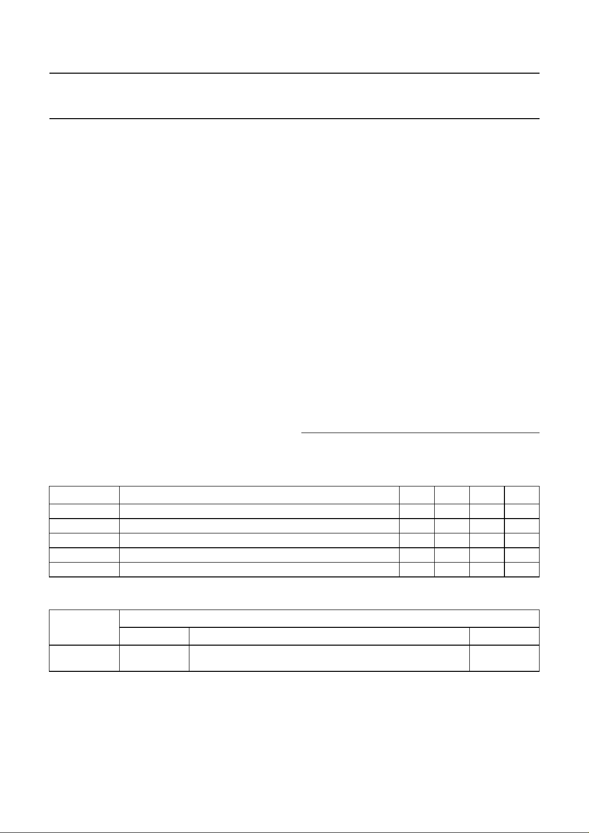
5 BLOCK DIAGRAMS
Philips Semiconductors Product specification
Field and line rate converter
with noise reduction
YA0 to YA7
SNCL
SNDA
SNRST
TCK
TDO
TDI
TMS
TRST
TE
CLK32
45 to 52
27
26
25
35
34
33
32
31
30
79
SNERT
INTERFACE
CONTROL
BST/TEST
DYNAMIC
NOISE
REDUCTION
MPR
LEFT
FIELD MEMORY 2
YB7 to YB0
151, 152,
154 to 159
COMPRESS
MUX
MUX
DE-INTERLACER
vectors
SPM TPM ESM
MOTION ESTIMATOR
vectors
UPCONVERSION
YC0 to YC7
2 to 9
DECOMPRESS
FIELD MEMORY 3
YD7 to YD0
111, 112,
114 to 119
MPR
RIGHT
VERTICAL
PEAKING
YE0 to YE7
122 to 129
SEQUENCER
SAA4993H
VERTICAL
ZOOM
61 to 68
82 to 89
YF7 to YF0
YG7 to YG0
The solid lines represent pixel data; the broken lines represent controls.
Fig.1 Block diagram of the luminance part.
MHC054
SAA4993H
This text is here in white to force landscape pages to be rotated correctly when browsing through the pdf in the Acrobat reader.This text is here in
_white to force landscape pages to be rotated correctly when browsing through the pdf in the Acrobat reader.This text is here inThis text is here in
white to force landscape pages to be rotated correctly when browsing through the pdf in the Acrobat reader. white to force landscape pages to be ...
2001 Nov 23 5
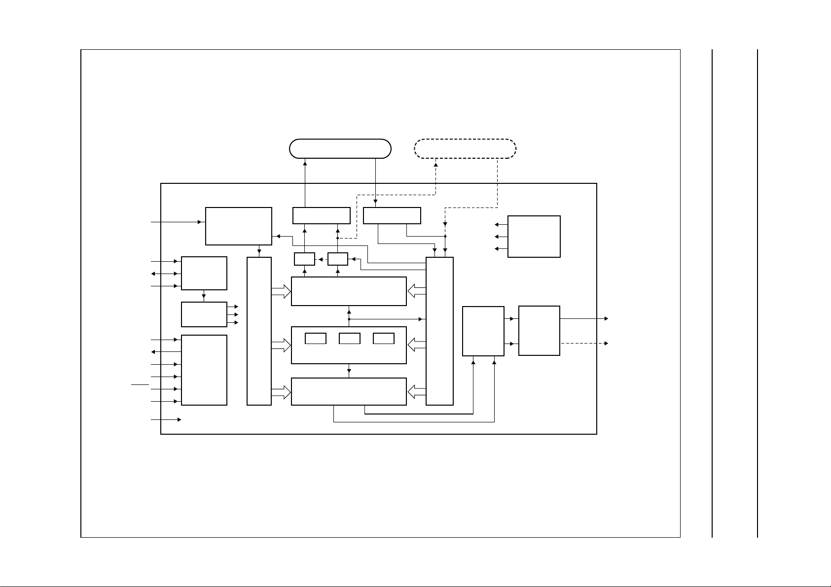
FIELD MEMORY 2 FIELD MEMORY 3
handbook, full pagewidth
Philips Semiconductors Product specification
Field and line rate converter
with noise reduction
UVA0 to UVA7
37 to 44
DECOMPRESS/
REFORMAT
DNR
MPR
LEFT
UVB3 to UVB0
147 to 150
COMPRESS/
FORMAT
UPCONVERSION
vectors
UVC0 to UVC3
10 to 13
DECOMPRESS/
REFORMAT
MPR
RIGHT
UVD3 to UVD0
107 to 110
SAA4993H
VERTICAL
ZOOM
UVE0 to UVE3
130 to 133
FORMAT
70 to 77
91 to 98
MHC055
UVF7 to YVF0
UVG7 to YVG0
SAA4993H
The solid lines represent pixel data; the broken lines represent the data flow, if the (optional) field memory 3 is also used.
Fig.2 Block diagram of the chrominance part.
Philips Semiconductors Product specification
Field and line rate converter
SAA4993H
with noise reduction
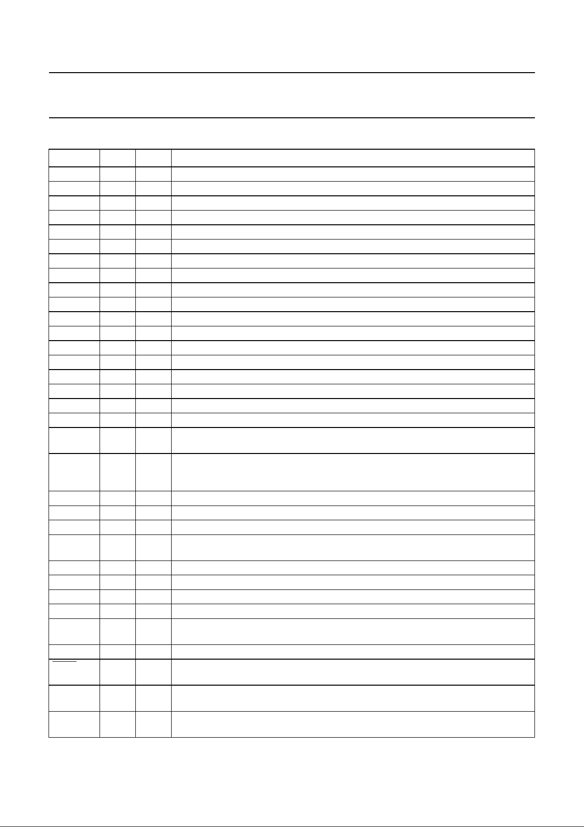
6 PINNING
SYMBOL PIN TYPE DESCRIPTION
V
SSE
1 ground ground of output pads
YC0 2 input bus C luminance input from field memory 2 bit 0 (LSB)
YC1 3 input bus C luminance input from field memory 2 bit 1
YC2 4 input bus C luminance input from field memory 2 bit 2
YC3 5 input bus C luminance input from field memory 2 bit 3
YC4 6 input bus C luminance input from field memory 2 bit 4
YC5 7 input bus C luminance input from field memory 2 bit 5
YC6 8 input bus C luminance input from field memory 2 bit 6
YC7 9 input bus C luminance input from field memory 2 bit 7 (MSB)
UVC0 10 input bus C chrominance input from field memory 2 bit 0 (LSB)
UVC1 11 input bus C chrominance input from field memory 2 bit 1
UVC2 12 input bus C chrominance input from field memory 2 bit 2
UVC3 13 input bus C chrominance input from field memory 2 bit 3 (MSB)
REC 14 output read enable output for busC
V
V
V
V
SSE
DDE
SSI
DDI
15 ground ground of output pads
16 supply external supply voltage (output pads)
17 ground core ground
18 supply core supply voltage
JUMP0 19 input configuration pin 0; will be stored in register 0B3 e.g. to indicate presence of 3rd field
memory; should be connected to ground or to V
JUMP1 20 input configuration pin 1; will be stored in register 0B5 e.g. to indicate presence of 16-bit
1st field memory for full 4:2:2;should be connected to ground or to V
resistor of 47 kΩ
V
V
V
DDE
DDI
SSI
21 supply external supply voltage (output pads)
22 supply core supply voltage
23 ground core ground
RAMTST1 24 input test pin 1 input for internal RAM testing with internal pull-down; connect to ground for
normal operation
SNRST 25 input SNERT bus reset input
SNDA 26 I/O SNERT bus data input and output
SNCL 27 input SNERT bus clock input
V
SSE
28 ground ground of output pads
RAMTST2 29 input test pin 2 input for internal RAM testing with internal pull-down; connect to ground for
normal operation
TE 30 input test mode input with internal pull-down; if not used it has to be connected to ground
TRST 31 input boundary scan test reset input (active LOW); if not used it has to be connected to V
via a pull-up resistor of 47 kΩ
TMS 32 input boundary scan test mode select input; if not used it has to be connected to V
pull-up resistor of 47 kΩ
TDI 33 input boundary scan test data input; if not used it has to be connected to V
resistor of 47 kΩ
(1)(2)
via a pull-up resistor of 47 kΩ
DDE
DDE
DDE
via a pull-up
via a
DDE
via a pull-up
DDE
2001 Nov 23 6

Philips Semiconductors Product specification
Field and line rate converter
with noise reduction
SYMBOL PIN TYPE DESCRIPTION
TDO 34 3-state boundary scan test data output
TCK 35 input boundary scan test clock input; if not used it has to be connected to V
resistor of 47 kΩ
V
SSE
36 ground ground of output pads
UVA0 37 input bus A chrominance input from field memory 1 bit 0 (LSB)
UVA1 38 input bus A chrominance input from field memory 1 bit 1
UVA2 39 input bus A chrominance input from field memory 1 bit 2
UVA3 40 input bus A chrominance input from field memory 1 bit 3
UVA4 41 input bus A chrominance input from field memory 1 bit 4
UVA5 42 input bus A chrominance input from field memory 1 bit 5
UVA6 43 input bus A chrominance input from field memory 1 bit 6
UVA7 44 input bus A chrominance input from field memory 1 bit 7 (MSB)
YA0 45 input bus A luminance input from field memory 1 bit 0 (LSB)
YA1 46 input bus A luminance input from field memory 1 bit 1
YA2 47 input bus A luminance input from field memory 1 bit 2
YA3 48 input bus A luminance input from field memory 1 bit 3
YA4 49 input bus A luminance input from field memory 1 bit 4
YA5 50 input bus A luminance input from field memory 1 bit 5
YA6 51 input bus A luminance input from field memory 1 bit 6
YA7 52 input bus A luminance input from field memory 1 bit 7 (MSB)
REA 53 output read enable output for bus A
V
V
V
V
V
V
SSE
SSI
DDI
DDI
SSI
SSE
54 ground ground of output pads
55 ground core ground
56 supply core supply voltage
57 supply core supply voltage
58 ground core ground
59 ground ground of output pads
REF 60 input read enable input for bus F and G
YF7 61 output bus F luminance output bit 7 (MSB)
YF6 62 output bus F luminance output bit 6
YF5 63 output bus F luminance output bit 5
YF4 64 output bus F luminance output bit 4
YF3 65 output bus F luminance output bit 3
YF2 66 output bus F luminance output bit 2
YF1 67 output bus F luminance output bit 1
YF0 68 output bus F luminance output bit 0 (LSB)
V
DDE
69 supply external supply voltage (output pads)
UVF7 70 output bus F chrominance output bit 7 (MSB)
UVF6 71 output bus F chrominance output bit 6
UVF5 72 output bus F chrominance output bit 5
UVF4 73 output bus F chrominance output bit 4
(1)(2)
SAA4993H
via a pull-up
DDE
2001 Nov 23 7
Philips Semiconductors Product specification
Field and line rate converter
with noise reduction
SYMBOL PIN TYPE DESCRIPTION
UVF3 74 output bus F chrominance output bit 3
UVF2 75 output bus F chrominance output bit 2
UVF1 76 output bus F chrominance output bit 1
UVF0 77 output bus F chrominance output bit 0 (LSB)
V
SSE
78 ground ground of output pads
CLK32 79 input system clock input
V
V
SSI
SSE
80 ground core ground
81 ground ground of output pads
YG7 82 3-state bus G luminance output bit 7 (MSB)
YG6 83 3-state bus G luminance output bit 6
YG5 84 3-state bus G luminance output bit 5
YG4 85 3-state bus G luminance output bit 4
YG3 86 3-state bus G luminance output bit 3
YG2 87 3-state bus G luminance output bit 2
YG1 88 3-state bus G luminance output bit 1
YG0 89 3-state bus G luminance output bit 0 (LSB)
V
DDE
90 supply external supply voltage (output pads)
UVG7 91 3-state bus G chrominance output bit 7 (MSB) or vector output bit 7
UVG6 92 3-state bus G chrominance output bit 6 or vector output bit 6
UVG5 93 3-state bus G chrominance output bit 5 or vector output bit 5
UVG4 94 3-state bus G chrominance output bit 4 or vector output bit 4
UVG3 95 3-state bus G chrominance output bit 3 or vector output bit 3
UVG2 96 3-state bus G chrominance output bit 2 or vector output bit 2
UVG1 97 3-state bus G chrominance output bit 1 or vector output bit 1
UVG0 98 3-state bus G chrominance output bit 0 (LSB) or vector output bit 0
V
V
V
V
V
V
V
SSE
SSI
DDI
DDE
DDI
SSI
SSE
99 ground ground of output pads
100 ground core ground
101 supply core supply voltage
102 supply external supply voltage (output pads)
103 supply core supply voltage
104 ground core ground
105 ground ground of output pads
WED 106 3-state write enable output for bus D
UVD3 107 3-state bus D chrominance output to field memory 3 bit 3 (MSB)
UVD2 108 3-state bus D chrominance output to field memory 3 bit 2
UVD1 109 3-state bus D chrominance output to field memory 3 bit 1
UVD0 110 3-state bus D chrominance output to field memory 3 bit 0 (LSB)
YD7 111 3-state bus D luminance output to field memory 3 bit 7 (MSB)
YD6 112 3-state bus D luminance output to field memory 3 bit 6
V
DDE
113 supply external supply voltage (output pads)
YD5 114 3-state bus D luminance output to field memory 3 bit 5
(1)(2)
SAA4993H
2001 Nov 23 8
Philips Semiconductors Product specification
Field and line rate converter
SAA4993H
with noise reduction
SYMBOL PIN TYPE DESCRIPTION
YD4 115 3-state bus D luminance output to field memory 3 bit 4
YD3 116 3-state bus D luminance output to field memory 3 bit 3
YD2 117 3-state bus D luminance output to field memory 3 bit 2
YD1 118 3-state bus D luminance output to field memory 3 bit 1
YD0 119 3-state bus D luminance output to field memory 3 bit 0 (LSB)
V
V
SSE
SSE
120 ground ground of output pads
121 ground ground of output pads
YE0 122 input bus E luminance input from field memory 3 bit 0 (LSB)
YE1 123 input bus E luminance input from field memory 3 bit 1
YE2 124 input bus E luminance input from field memory 3 bit 2
YE3 125 input bus E luminance input from field memory 3 bit 3
YE4 126 input bus E luminance input from field memory 3 bit 4
YE5 127 input bus E luminance input from field memory 3 bit 5
YE6 128 input bus E luminance input from field memory 3 bit 6
YE7 129 input bus E luminance input from field memory 3 bit 7 (MSB)
UVE0 130 input bus E chrominance input from field memory 3 bit 0 (LSB)
UVE1 131 input bus E chrominance input from field memory 3 bit 1
UVE2 132 input bus E chrominance input from field memory 3 bit 2
UVE3 133 input bus E chrominance input from field memory 3 bit 3 (MSB)
REE 134 output read enable output for bus E
V
SSE
135 ground ground of output pads
HREF 136 input horizontal reference synchronization input
V
SSI
V
DDI
137 ground core ground
138 supply core supply voltage
OSCI 139 input test pin input with internal pull-down; connect to ground for normal operation
RESFM 140 output reset field memory output for pin OSCI = LOW or test output OSCOUT for
pin OSCI = HIGH
V
V
V
DDE
DDI
SSI
141 supply external supply voltage (output pads)
142 supply core supply voltage
143 ground core ground
ACV 144 output active video output
V
SSE
145 ground ground of output pads
WEB 146 output write enable output for bus B
UVB3 147 output bus B chrominance output to field memory 2 bit 3 (MSB)
UVB2 148 output bus B chrominance output to field memory 2 bit 2
UVB1 149 output bus B chrominance output to field memory 2 bit 1
UVB0 150 output bus B chrominance output to field memory 2 bit 0 (LSB)
YB7 151 output bus B luminance output to field memory 2 bit 7 (MSB)
YB6 152 output bus B luminance output to field memory 2 bit 6
V
DDE
153 supply external supply voltage (output pads)
YB5 154 output bus B luminance output to field memory 2 bit 5
(1)(2)
2001 Nov 23 9

Philips Semiconductors Product specification
Field and line rate converter
SAA4993H
with noise reduction
SYMBOL PIN TYPE DESCRIPTION
YB4 155 output bus B luminance output to field memory 2 bit 4
YB3 156 output bus B luminance output to field memory 2 bit 3
YB2 157 output bus B luminance output to field memory 2 bit 2
YB1 158 output bus B luminance output to field memory 2 bit 1
YB0 159 output bus B luminance output to field memory 2 bit 0 (LSB)
V
SSE
Notes
1. Not used input pins (e.g. bus E) should be connected to ground.
2. Because of the noisy characteristic of the output pad supply, it is recommended not to connect the core supply and
the output pad supply directly at the device. The output pad supply should be buffered as close as possible to the
device.
160 ground ground of output pads
(1)(2)
2001 Nov 23 10
Philips Semiconductors Product specification
Field and line rate converter
with noise reduction
handbook, full pagewidth
V
SSE
YC0
YC1
YC2
YC3
YC4
YC5
YC6
YC7
UVC0
UVC1
UVC2
UVC3
REC
V
SSE
V
DDE
V
SSI
V
DDI
JUMP0
JUMP1
V
DDE
V
DDI
V
SSI
RAMTST1
SNRST
SNDA
SNCL
V
SSE
RAMTST2
TE
TRST
TMS
TDI
TDO
TCK
V
SSE
UVA0
UVA1
UVA2
UVA3
SSE
V
YB0
YB1
YB2
160
159
158
157
1
2
3
4
5
6
7
8
9
10
11
12
13
14
15
16
17
18
19
20
21
22
23
24
25
26
27
28
29
30
31
32
33
34
35
36
37
38
39
40
YB3
156
YB4
155
YB5
154
DDE
V
153
YB6
152
YB7
151
UVB0
150
UVB1
149
UVB2
148
UVB3
147
WEB
146
V
145
SSE
SSIVDDI
DDE
ACV
V
V
144
143
142
141
SAA4993H
RESFM
OSCI
140
139
DDIVSSI
V
138
137
HREF
V
136
SSE
135
REE
134
UVE3
133
UVE2
132
UVE1
131
UVE0
130
YE7
129
YE6
128
YE5
127
YE4
126
SAA4993H
YE2
124
YE1
123
YE0
122
V
121
SSE
YE3
125
120
119
118
117
116
115
114
113
112
111
110
109
108
107
106
105
104
103
102
101
100
99
98
97
96
95
94
93
92
91
90
89
88
87
86
85
84
83
82
81
V
SSE
YD0
YD1
YD2
YD3
YD4
YD5
V
DDE
YD6
YD7
UVD0
UVD1
UVD2
UVD3
WED
V
SSE
V
SSI
V
DDI
V
DDE
V
DDI
V
SSI
V
SSE
UVG0
UVG1
UVG2
UVG3
UVG4
UVG5
UVG6
UVG7
V
DDE
YG0
YG1
YG2
YG3
YG4
YG5
YG6
YG7
V
SSE
414243444546474849505152535455565758596061626364656667686970717273747576777879
SSI
SSI
UVA4
UVA5
UVA6
UVA7
YA0
YA1
YA2
YA3
YA4
YA5
YA6
YA7
REA
SSE
V
DDIVDDI
V
SSE
V
V
V
Fig.3 Pin configuration.
2001 Nov 23 11
REF
YF7
YF6
YF5
YF4
YF3
YF2
YF1
YF0
DDE
V
UVF7
UVF6
UVF5
UVF4
UVF3
UVF2
UVF1
UVF0
SSE
V
80
SSI
V
CLK32
MHC056
Philips Semiconductors Product specification
Field and line rate converter
with noise reduction
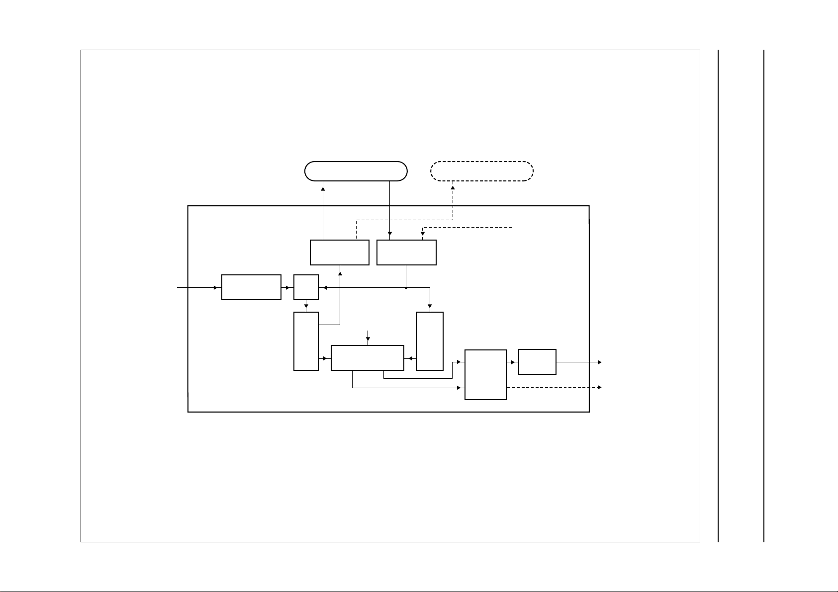
7 FUNCTIONAL DESCRIPTION
The fal_top module builds the functional top level of the
SAA4993H. It connects the luminance data path, the
chrominance data path and the luminance
(de)compression with SAA4993H inputs and outputs as
well as controlling logic. Outside of the fal_top module,
there are only the pad cells, boundary scan test cells, the
boundary scan test controller, the clock tree, the test
enable tree and the input port registers.
Figure 4 shows a simplified block diagram of the fal_top
module. It displays the flow of pixel data (solid lines) and
controls (broken lines) between the modules inside.
Basic functionality of the modules in the fal_top module is
as follows:
• KER (kernel): Y (luminance) data path
• COL (colour): UV (chrominance) data path
• YDP (Y-DPCM): compression (and decompression) of
luminance output (and input) data by Differential Pulse
Code Modulation (DPCM)
• LSE (line sequencer): generate line frequent control
signals
• SNE (interface): Synchronous No parity Eight bit
Reception and Transmission (SNERT) interface to a
microcontroller.
The SNERT interface operates in a slave receive and
transmit mode for communication with a microcontroller,
which resides on peripheral circuits (e.g. SAA4978H)
together with a SNERT master. The SNERT interface
transforms serial data from the microcontroller (via the
SNERT bus) into parallel data to be written into the
SAA4993Hs write registers and parallel data from
SAA4993Hsreadregistersintoserialdatatobesenttothe
microcontroller. The SNERT bus consists of 3 signals:
1. SNCL: used as serial clock signal, generated by the
master
2. SNDA: used as bidirectional data line
3. SNRST: used as a reset signal, generated by the
microcontroller to indicate the start of a transmission.
SAA4993H
Table 1 Clock cycle references
SIGNAL LATENCY
RE_F 0
RE_C and
RE_E
YC, YE, UVC
and UVE
RE_A 93 cycles + REaShift
YA and UVA 94 cycles
YF, YG, UVF
and UVG
WE_B and
WE_D
YB, YD, UVB
and UVD
There is an algorithmic delay of 3 lines between input and
output data. Therefore, the main data output on the
F and G bus begins while the fourth input line is read.
Writing to the B and D bus starts one input line later. The
readandwriteenablesignalsRE_A,WE_B,RE_C,WE_D
and RE_E can be shifted by control registers REaShift,
WEbdShift and REceShift, which are implemented in the
line sequencer.
The fal_top module itself reads the following control
register bits (addresses):
• NrofFMs (017H)
• MatrixOn (026H) and BusGControl (028H)
• MemComp and MemDecom (026H).
NrofFMs, MatrixOn and BusGControl are used to enable
the D and G output bus, respectively. MemComp and
MemDecom are connected to YDP to control luminance
data compression and decompression. These control
register signals are not displayed in Fig.4. Further
information on the control registers is given in Chapter 8.
62 cycles + REceShift
63 cycles
147 cycles + 3 input lines
159 cycles + 4 input lines + WEbdShift
159 cycles + 4 input lines
The processing of a video field begins on the rising edge
of the RE_F input signal. As indicated in Fig.4, the
SAA4993H receives its inputs and generatesits outputs at
the following clock cycles after RE_F (see Table 1).
2001 Nov 23 12
 Loading...