

Philips SAA4990H-V0, SAA4990H-V1, SAA4990H-V2 Datasheet

DATA SH EET
Preliminary specification
File under Integrated Circuits, IC02
1996 Oct 25
INTEGRATED CIRCUITS
SAA4990H
Progressive scan-Zoom and Noise
reduction IC (PROZONIC)
1996 Oct 25 2
Philips Semiconductors Preliminary specification
Progressive scan-Zoom and Noise
reduction IC (PROZONIC)
SAA4990H
FEATURES
• Progressive scan conversion
(262.5 to 525 or 312.5 to 625 lines/field)
• Field rate up-conversion (50 to 100 Hz or 60 to 120 Hz)
• Line flicker reduction
• Noise and cross-colour reduction
• Variable vertical sample rate conversion
• Movie phase detection
• Synchronous No parity Eight bit Reception and
Transmission (SNERT) interface.
GENERAL DESCRIPTION
The Progressive scan-Zoom and Noise reduction IC,
abbreviated as PROZONIC, is designed for applications
together with:
SAA4951WP Economy Controller (ECO3)
SAA4952H (memory controller)
SAA7158WP Back END IC (BENDIC)
SAA4995WP PANorama IC (PANIC)
SAA4970T ECOnomical video processing Back END IC
(ECOBENDIC)
TMS4C2970/71 (serial field memories)
TDA8755/8753A (A/D converter 4 : 1 : 1 format)
83C652/54 type of microcontroller.
QUICK REFERENCE DATA
ORDERING INFORMATION
SYMBOL PARAMETER MIN. MAX. UNIT
V
DDD
digital supply voltage 4.5 5.5 V
T
amb
operating ambient temperature 0 70 °C
TYPE
NUMBER
PACKAGE
NAME DESCRIPTION VERSION
SAA4990H QFP80 plastic quad flat package; 80 leads (lead length 1.95 mm); body 14 × 20 × 2.8 mm SOT318-2

1996 Oct 25 3
Philips Semiconductors Preliminary specification
Progressive scan-Zoom and Noise
reduction IC (PROZONIC)
SAA4990H
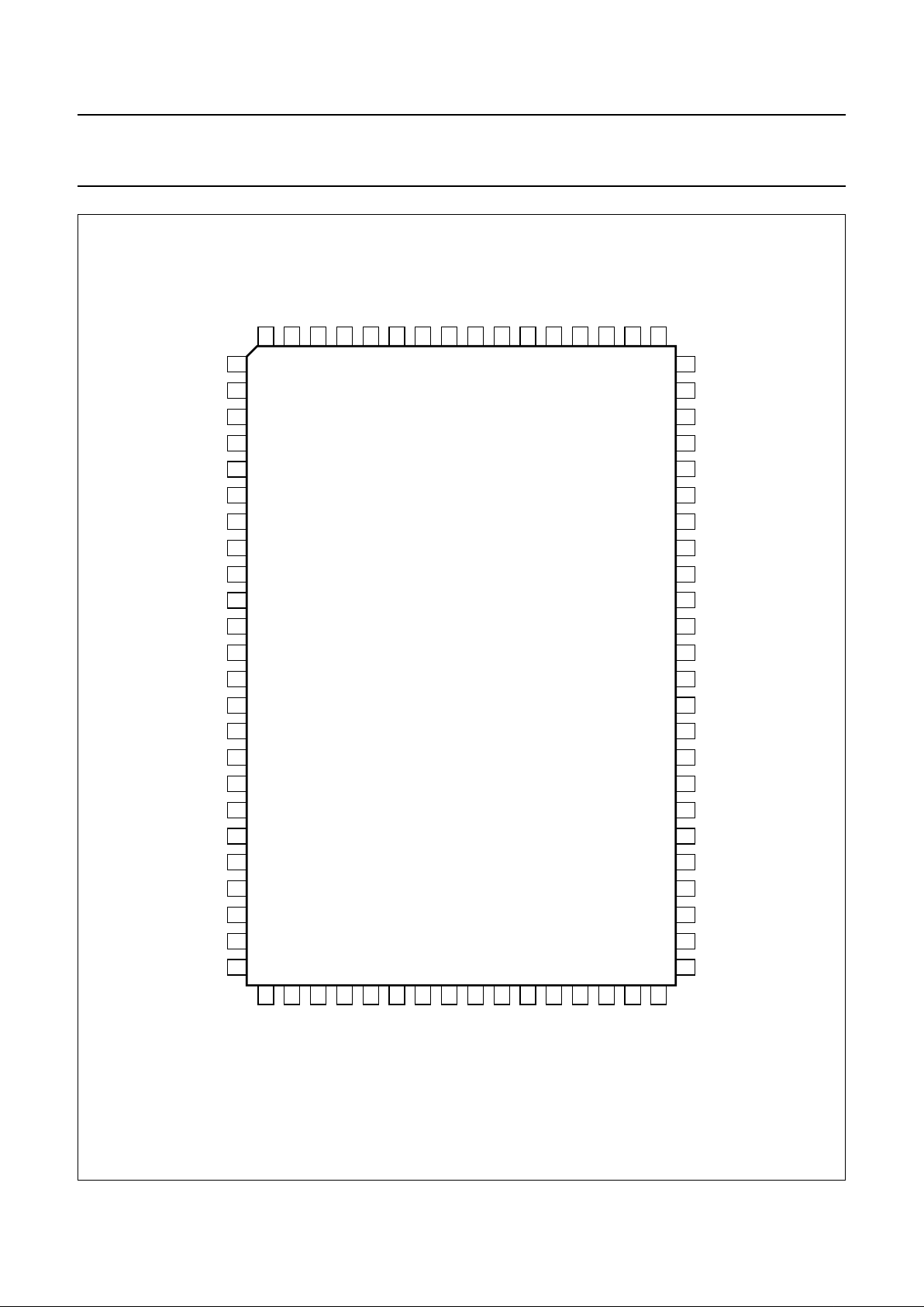
BLOCK DIAGRAM
d
book, full pagewidth
MGE024
REFORMATTER
REFORMATTER
FORMATTER
CONTROL BLOCK
SNCL, SNDA,
SNRST
CK RE, WEVD, HD
FORMATTER
NOISE
REDUCTION
NOISE
REDUCTION
LINE
MEMORY 1
LINE
MEMORY 2
MIXER
LINE
MEMORY 3
MIXER
LINE
MEMORY 1
LINE
MEMORY 2
MEDIAN
FILTER
LINE
MEMORY 3
MIXER
MOVIE
PHASE
DETECTOR
MICROPROCESSOR
INTERFACE
(SNERT)
UV1
UV2
Y1
Y2
4
4
3
RE1
RE2
WE2
12
YUV
D
12
12
12
YUV
A
YUV
B
YUV
C
8
84
8
8
3 2 2
SAA4990H
Fig.1 Block diagram.

1996 Oct 25 4
Philips Semiconductors Preliminary specification
Progressive scan-Zoom and Noise
reduction IC (PROZONIC)
SAA4990H
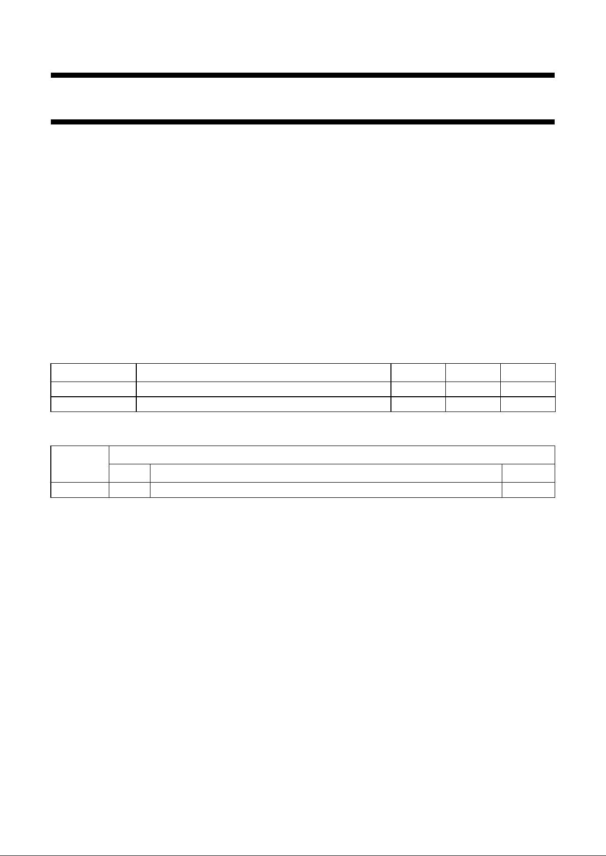
PINNING
SYMBOL PIN TYPE DESCRIPTION
TEST1/AP 1 input action pin for testing, to be connected to V
SS
TEST2/SP 2 input shift pin for testing, to be connected to V
SS
RE1 3 output read enable to FM1
V
SS1
4 ground ground 1
V
DD1
5 supply supply voltage 1
YUV
C7
6 output Y bit 7 to FM2
YUV
C6
7 output Y bit 6 to FM2
YUV
C5
8 output Y bit 5 to FM2
YUV
C4
9 output Y bit 4 to FM2
YUV
C3
10 output Y bit 3 to FM2
V
SS2
11 ground ground 2
V
DD2
12 supply supply voltage 2
YUV
C2
13 output Y bit 2 to FM2
YUV
C1
14 output Y bit 1 to FM2
YUV
C0
15 output Y bit 0 to FM2
YUV
C11
16 output UV bit 3 to FM2
YUV
C10
17 output UV bit 2 to FM2
YUV
C9
18 output UV bit 1 to FM2
YUV
C8
19 output UV bit 0 to FM2
CK 20 input master clock, nominal 27 or 32 MHz
V
SS3
21 ground ground 3
V
DD3
22 supply supply voltage 3
WE2 23 output write enable to FM2
RE2 24 output read enable to FM2
YUV
B8
25 input UV bit 0 from FM2
YUV
B9
26 input UV bit 1 from FM2
YUV
B10
27 input UV bit 2 from FM2
YUV
B11
28 input UV bit 3 from FM2
YUV
B0
29 input Y bit 0 from FM2
YUV
B1
30 input Y bit 1 from FM2
YUV
B2
31 input Y bit 2 from FM2
YUV
B3
32 input Y bit 3 from FM2
V
DD4
33 supply supply voltage 4
V
SS4
34 ground ground 4
YUV
B4
35 input Y bit 4 from FM2
YUV
B5
36 input Y bit 5 from FM2
YUV
B6
37 input Y bit 6 from FM2
YUV
B7
38 input Y bit 7 from FM2
RE 39 input master read enable
VD 40 input field frequent reset, vertical display

1996 Oct 25 5
Philips Semiconductors Preliminary specification
Progressive scan-Zoom and Noise
reduction IC (PROZONIC)
SAA4990H
HD 41 input horizontal reference signal
YUV
D8
42 output UV bit 0
YUV
D9
43 output UV bit 1
YUV
D10
44 output UV bit 2
V
DD5
45 supply supply voltage 5
V
SS5
46 ground ground 5
YUV
D11
47 output UV bit 3
YUV
D0
48 output Y bit 0
YUV
D1
49 output Y bit 1
YUV
D2
50 output Y bit 2
V
DD6
51 supply supply voltage 6
V
SS6
52 ground ground 6
YUV
D3
53 output Y bit 3
YUV
D4
54 output Y bit 4
YUV
D5
55 output Y bit 5
YUV
D6
56 output Y bit 6
YUV
D7
57 output Y bit 7
V
DD7
58 supply supply voltage 7
V
SS7
59 ground ground 7
SNRST 60 input field frequent reset from microcontroller; reset for SNERT interface
SNDA 61 I/O data for SNERT interface
SNCL 62 input clock for SNERT interface
AUX 63 output spare output from line-sequencer
H
O
64 output output hold to e.g. LC display
n.c. 65 − not connected
n.c. 66 − not connected
YUV
A7
67 input Y bit 7 from FM1
YUV
A6
68 input Y bit 6 from FM1
YUV
A5
69 input Y bit 5 from FM1
YUV
A4
70 input Y bit 4 from FM1
YUV
A3
71 input Y bit 3 from FM1
YUV
A2
72 input Y bit 2 from FM1
V
SS8
73 ground ground 8
V
DD8
74 supply supply voltage 8
YUV
A1
75 input Y bit 1 from FM1
YUV
A0
76 input Y bit 0 from FM1
YUV
A11
77 input UV bit 3 from FM1
YUV
A10
78 input UV bit 2 from FM1
YUV
A9
79 input UV bit 1 from FM1
YUV
A8
80 input UV bit 0 from FM1
SYMBOL PIN TYPE DESCRIPTION
1996 Oct 25 6
Philips Semiconductors Preliminary specification
Progressive scan-Zoom and Noise
reduction IC (PROZONIC)
SAA4990H
Fig.2 Pin configuration.
handbook, full pagewidth
SAA4990H
MGE023
1
2
3
4
5
6
7
8
9
10
11
12
13
14
15
16
17
18
19
20
60
59
58
57
56
64
63
62
61
55
54
53
52
51
50
49
48
47
46
45
44
43
42
41
21
22
23
24
TEST1/AP
TEST2/SP
RE1
V
SS1
V
DD1
YUV
C7
YUV
C6
YUV
C5
YUV
C4
YUV
C3
V
SS2
V
DD2
YUV
C2
YUV
C1
YUV
C0
YUV
C11
YUV
C10
YUV
C9
YUV
C8
V
SS3
V
DD3
CK
WE2
RE2
YUVB8YUV
B9
YUV
B10
YUV
B11
YUVB0YUVB1YUVB2YUV
B3
V
DD4
V
SS4
YUVB4YUVB5YUVB6YUV
B7
RE
VD
YUVA8YUVA9YUV
A10
YUV
A11
YUVA0YUVA1V
DD8VSS8
YUVA2YUVA3YUVA4YUVA5YUVA6YUVA7n.c.
n.c.
H
O
AUX
SNCL
SNDA
SNRST
V
SS7
V
DD7
YUV
D7
YUV
D6
YUV
D5
YUV
D4
YUV
D3
V
SS6
V
DD6
YUV
D2
YUV
D1
YUV
D0
YUV
D11
V
SS5
V
DD5
YUV
D10
YUV
D9
YUV
D8
HD
25
26
27
28
29
30
31
32
33
34
35
36
37
38
39
40
80
79
78
77
76
75
74
73
72
71
70
69
68
67
66
65
1996 Oct 25 7
Philips Semiconductors Preliminary specification
Progressive scan-Zoom and Noise
reduction IC (PROZONIC)
SAA4990H
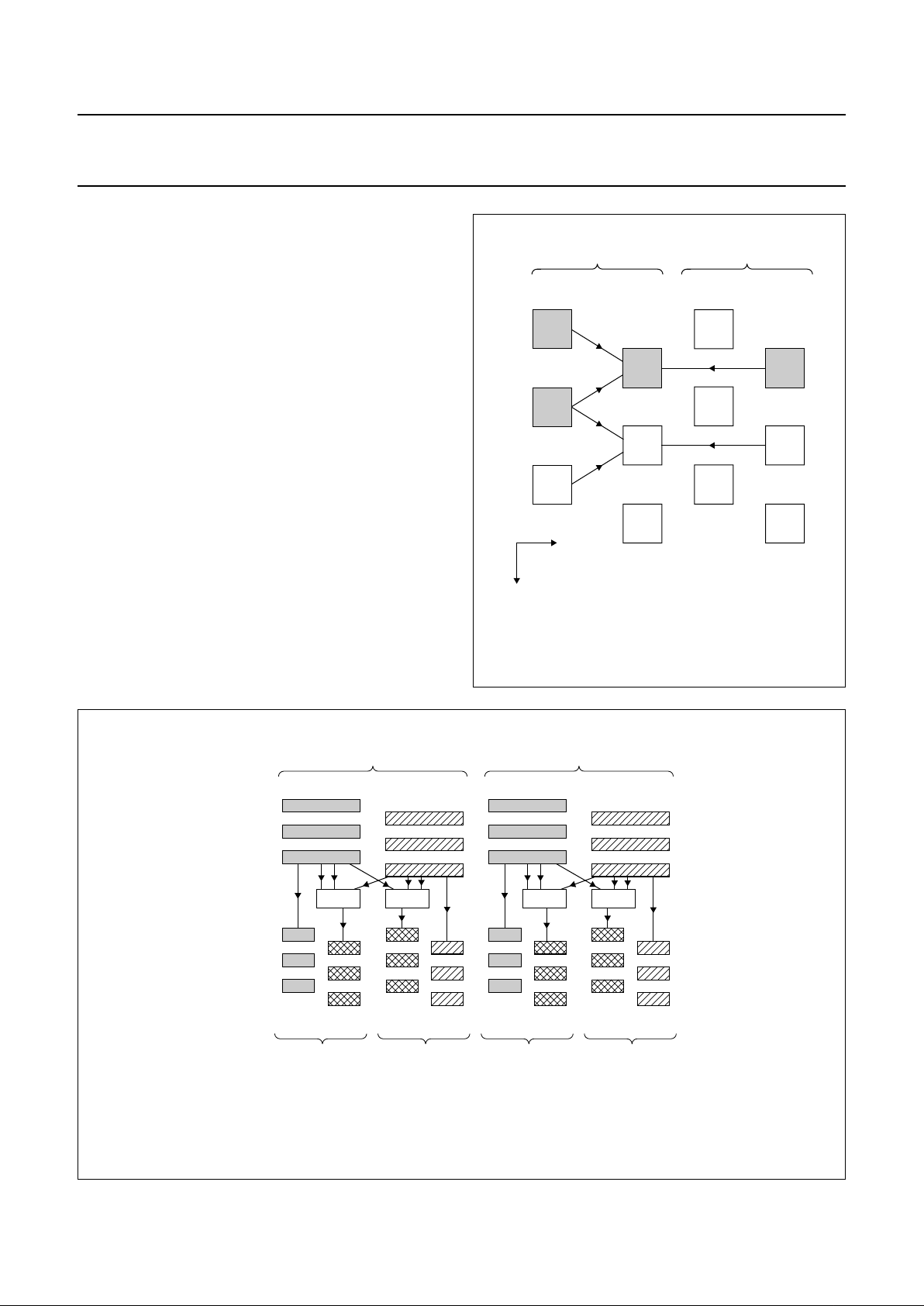
FUNCTIONAL DESCRIPTION
Field rate up-conversion with line flicker reduction
The line flicker reduction in conjunction with field rate
up-conversion is performed by generating a 50 Hz
interlace on the 100 Hz field rate display. Median filtering
supplies the data for the interlaced output fields.
D
EFINITIONS
Framel: l is the number of an input/output frame
temporarily combinating an A and B field.
: x is the field raster where A means an odd field and
B means an even field.
Frame
l, k
: l is the number of an output frame temporarily
combinating an origin/interpolated A and B field;
k indicates the origin input field with
k = 1: odd input field and raster A
k = 2: even input field and raster B within framel.
: n, m = lines of field
n, m
are interpolated by
2 lines of field
n
and 1 line of fieldm using the median filter
(see Fig.3); x is the field raster where A means an odd field
and B means an even field.
Field
n
x
Field
n, m
x
Fig.3 Generation of (median filter).field
n, m
B
handbook, halfpage
MGE026
t
y
frame
l, k = 1
field
A
n
field
B
m
frame
l, k = 2
field
B
n,m
field
A
m,n
Fig.4 Scan rate up-conversion.
handbook, full pagewidth
MGE027
input
1fH, 1f
v
output
2fH, 2f
v
frame
1, 1
frame
1, 2
frame
2, 1
field
A
4, 3
field
B
3, 4
field
A
3
field
A
3
field
B
2
field
B
2
field
A
2, 1
field
B
1, 2
field
A
1
field
A
1
field
B
4
field
B
4
frame
2, 2
frame
1
median
median
frame
2
median
median

1996 Oct 25 8
Philips Semiconductors Preliminary specification
Progressive scan-Zoom and Noise
reduction IC (PROZONIC)
SAA4990H
Progressive scan
Progressive scan conversion produces a double number
of lines per field on the output. The field frequency is not
changed, while the line frequency is doubled.
Processing for progressive scan is different for two
successive output fields, e.g. the first output field has a
median operation on the odd lines, while the second has
the median operation on the even lines.
NON-INTERLACE MODE
With non-interlaced progressive scan output, line flicker is
removed because interlace is removed.
I
NTERLACE MODE
With interlaced progressive scan the output line structure
and line flicker is less visible (projection TV).
P
ROGRESSIVE SCAN CONVERSION
Fig.5 Progressive scan conversion.
handbook, full pagewidth
MGE028
output
1fH, 1f
v
output
2fH, 1f
v
frame
1, 1
frame
1, 2
frame
2, 1
frame
2, 2
frame
1, 1
frame
1, 2
frame
2, 1
frame
2, 2
frame
1
median
a. Non-interlaced output; (625/50/1:1) or (525/60/1:1):
b. Interlaced output; (1250/50/2:1) or (1050/60/2:1):
median
frame
2
frame
1
frame
2
median
median
field
A
1
field
A
3
field
A
5
field
B
2
field
B
4
field
B
4
field
B
3, 4
field
A
3
field
A
2,3
field
B
2
field
B
1, 2
field
A
1
field
A
1,1
field
A
2,1
field
B
1,2
field
B
2,2
field
A
4,5
1996 Oct 25 9
Philips Semiconductors Preliminary specification
Progressive scan-Zoom and Noise
reduction IC (PROZONIC)
SAA4990H
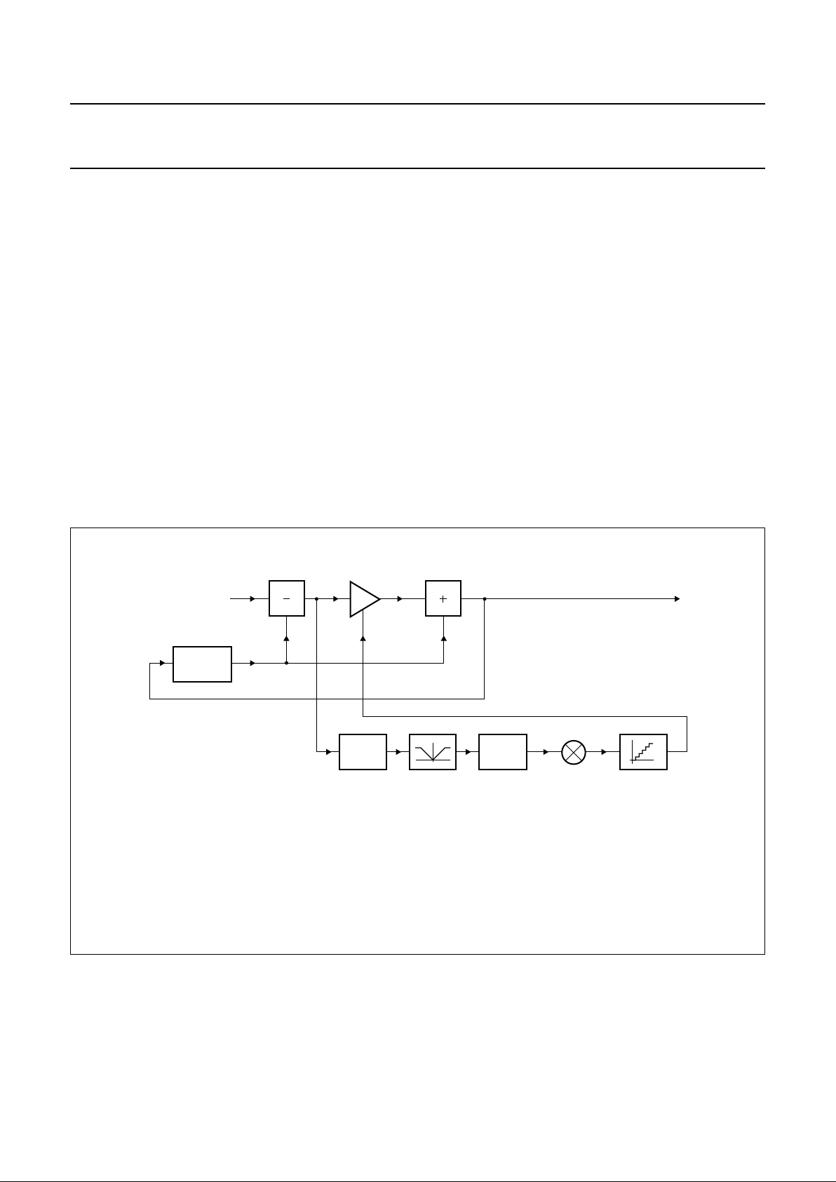
Noise and cross-colour reduction
The noise reduction is field recursive with an average ratio
between fresh and over previous fields averaged
luminance and chrominance.
Two operating modes can be used in principal: the fixed
and the adaptive mode (see Table 6).
In the fixed mode, the averaging produces a constant
linear combination of the inputs. Except for k = 1, the fixed
mode should not be used for normal operation, because of
its smearing effects.
In the adaptive mode, the averaging ratio switches softly
on the basis of absolute differences in luminance among
the inputs. When the absolute difference is low, only a
small part of the fresh data will be added. When the
difference is high, much of the fresh data will be taken.
This occurs in either the situation of movement or where a
significant vertical contrast is seen.
To latter remark, note that recursion is done over a field,
and the pixel positions one field apart always have a
vertical offset of one frame line. So averaging is not only
done in the dimension of time but also in the vertical
direction. Therefore averaging vertically on e.g. a vertical
black to white edge would provide a grey result if this was
not adapted for.
The averaging in chrominance is slaved to the luminance
averaging. This implies that differences in the
chrominance are not taken into account for the k-factor
setting.
The noise reduction scheme effectively decreases both
noise and cross-colour patterns.
The cross-colour pattern does not produce an increase of
the measured luminance difference, therefore this pattern
will be averaged over many fields.
Fig.6 Noise reduction scheme.
(1) Y
out=YA
×k+YB×(1 − k).
(2) see Table 9.
(3) see Fig.11.
handbook, full pagewidth
MGE029
FIELD
MEMORY
TF2TF1
FILTER LIMITER FILTER MULTIPLIER
(2)
k-CURVE
(3)
Y
out
(1)
Y
A
Y
B
k
 Loading...