

Philips SAA4981T, SAA4981 Datasheet
INTEGRATED CIRCUITS
DATA SH EET
SAA4981
Monolithic integrated 16 : 9
compressor
Preliminary specification
Supersedes data of May 1994
File under Integrated Circuits, IC02
1995 Oct 05
Philips Semiconductors Preliminary specification
Monolithic integrated 16 : 9 compressor SAA4981
FEATURES
• Fixed horizontal compression by a factor of4⁄3 for most
video standards
• Three fixed screen positions (left, centre and right)
• 5 MHz bandwidth
• Bypass function
• Inputs for luminance and chrominance of side panels
• Standard video inputs and outputs (Y, (B−Y) and (R−Y))
• Horizontal and vertical sync signals are not processed
• Pre filters and post filters on chip.
The synchronisation input HREF is a line frequency
reference signal. The bandwidth of the IC is up to 5 MHz
and the signal delay is realized with SC Line Memories
(Switched Capacitors Line Memories). The output of the
16 : 9 compressor also has the format Y, (B−Y) and (R−Y)
and provides the following two possibilities:
1. Bypass function (the input signal is not compressed)
2. Compressed video by a factor of
4
⁄3 with three different
fixed screen positions (left, centre and right). The
luminance and chrominance of the side panels are
determined by the external signals YSIDE, BYSIDE
and RYSIDE.
The horizontal compression is a time discrete and
GENERAL DESCRIPTION
The integrated 16 : 9 compressor is an IC which
compresses the active part of a video line by a factor of
from, for example, 52 µsto39µs. This is necessary to
display 4:3 video software on a 16 : 9 tube in the correct
proportion. The capacitively coupled video inputs are Y,
amplitude continuous signal processing. This provides pre
and post filters which are realized on-chip. The internal
clock generation is achieved with a 54 MHz horizontal PLL
4
⁄
3
which is synchronized to the positive edge of the HREF
signal. The function of the IC is controlled by the three
control signals CTRL1, CTRL2 and CTRL3.
(B−Y) and (R−Y).
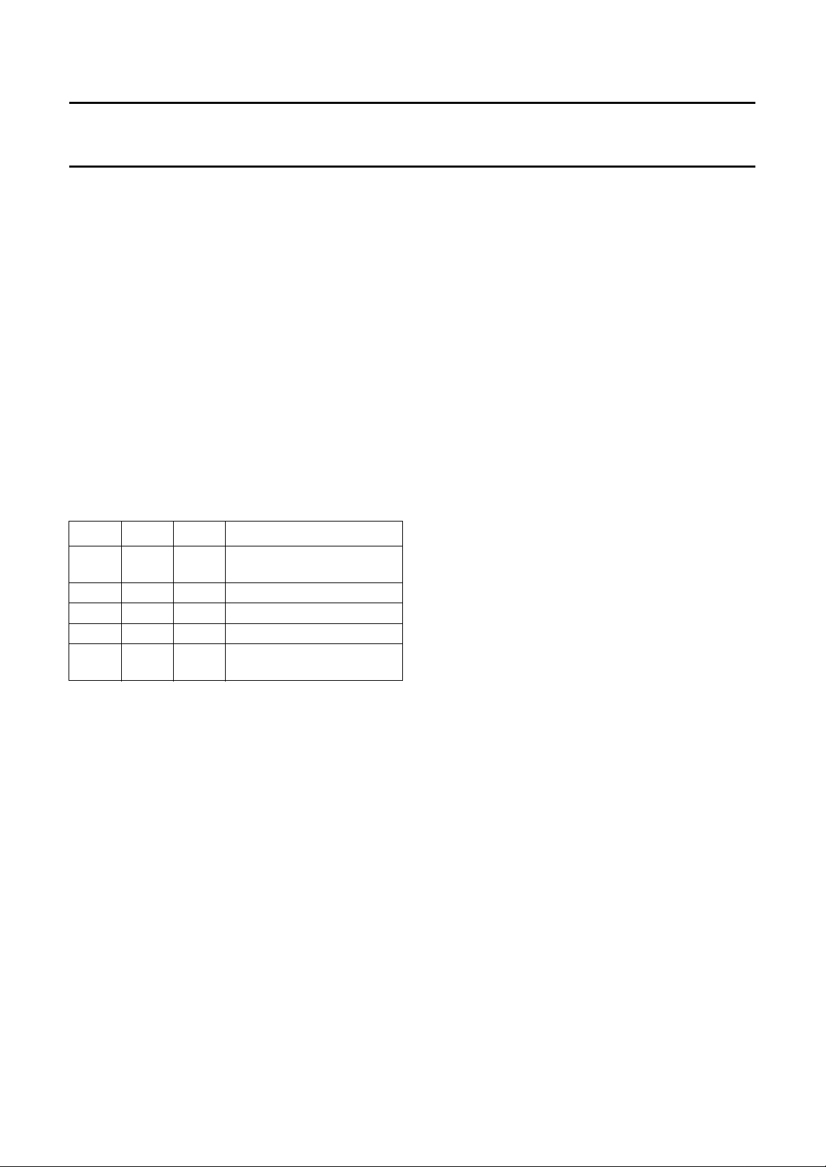
QUICK REFERENCE DATA
Voltages for video signals are peak-to-peak values for 75% colour bars. All voltages are referenced to
V
EEA=VEED
=0V.
SYMBOL PARAMETER MIN. TYP. MAX. UNIT
V
CCA
V
CCD
V
iY(p-p)
V
iU(p-p)
V
iV(p-p)
V
iHREF
V
oY(p-p)
V
oU(p-p)
V
oV(p-p)
analog supply voltage 4.75 5.0 5.5 V
digital supply voltage 4.75 5.0 5.5 V
Y input voltage (peak-to-peak value) − 0.32 0.45 V
(B−Y) input voltage (peak-to-peak value) − 1.33 1.9 V
(R−Y) input voltage (peak-to-peak value) − 1.05 1.5 V
input HREF top pulse 3.0 − 6.5 V
YOUT output voltage (peak-to-peak value) − 0.32 0.5 V
(B−Y)OUT output voltage (peak-to-peak value) − 1.33 2.1 V
(R−Y)OUT output voltage (peak-to-peak value) − 1.05 1.7 V
ORDERING INFORMATION
PACKAGE
TYPE NUMBER
NAME DESCRIPTION VERSION
SAA4981 DIP24 plastic dual in-line package; 24 leads (600 mil) SOT101-1
SAA4981T SO24 plastic small outline package; 24 leads; body width 7.5 mm SOT137-1
1995 Oct 05 2
Philips Semiconductors Preliminary specification
Monolithic integrated 16 : 9 compressor SAA4981
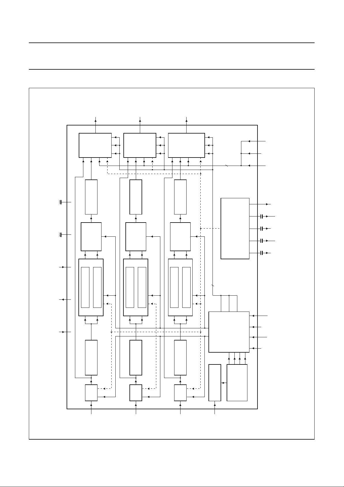
BLOCK DIAGRAM
V
V
SUB
EED
CCD
YOUT
18
MUX Y
6.7 MHz
LOW-PASS FILTER
MUX
SC LINE
MEMORIES
C1 C2 C3
SAA4981
(B-Y)OUT
17
MUX BY
6.7 MHz
LOW-PASS FILTER
MUX
SC LINE
MEMORIES
(R-Y)OUT
16
MUX RY
C1 C2 C3
6.7 MHz
LOW-PASS FILTER
MUX
SC LINE
MEMORIES
C1 C2 C3
3
CLAMP REFERENCE
MHA277
RYSIDE
BYSIDE
YSIDE
CLAOUT
BGREF
LMRY
C
LMBY
C
LMY
C
handbook, full pagewidth
V
V
EEA
CCA
20 19 8 7 4
SC LINE MEMORY
SC LINE MEMORY
5 MHz
LOW-PASS FILTER
CLAMP
23
YIN
SC LINE MEMORY
SC LINE MEMORY
5 MHz
LOW-PASS FILTER
CLAMP
22
(B-Y)IN
1995 Oct 05 3
SC LINE MEMORY
SC LINE MEMORY
5 MHz
LOW-PASS FILTER
CLAMP
21
(R-Y)IN
3
C1
HORIZONTAL
SEPARATION
6
HREF
C2
C3
CONTROLLER
PLL
54 MHz
Fig.1 Block diagram.
11 1 2 3 24 5 15 14 1310912
CTRL1 CTRL3
TEST CTRL2
Philips Semiconductors Preliminary specification
Monolithic integrated 16 : 9 compressor SAA4981
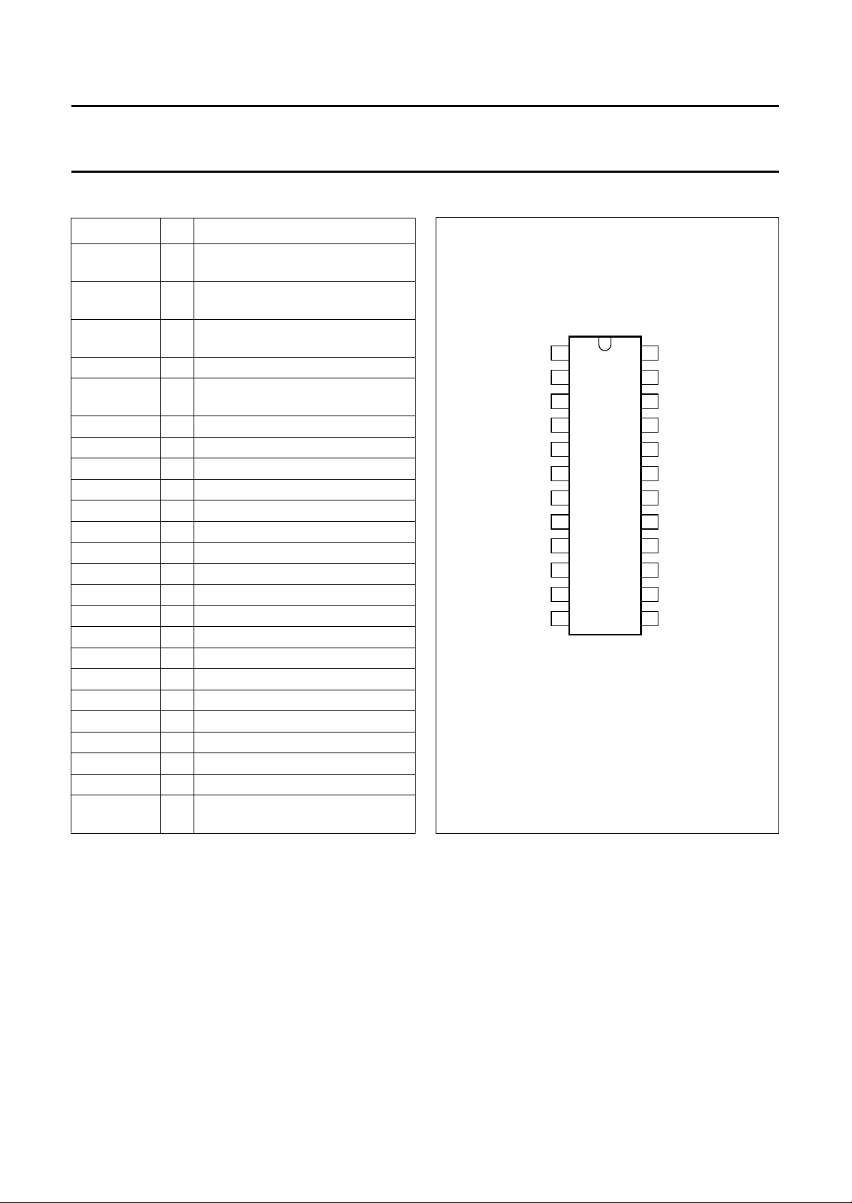
PINNING
SYMBOL PIN DESCRIPTION
C
LMY
C
LMBY
C
LMRY
SUB 4 substrate connection (see Fig.5)
CLAOUT 5 internal clamping reference voltage
HREF 6 horizontal reference input
V
EED
V
CCD
CTRL1 9 control input 1
CTRL2 10 control input 2
CTRL3 11 control input 3
TEST 12 test mode activation
RYSIDE 13 side panel input for RY
BYSIDE 14 side panel input for BY
YSIDE 15 side panel input for Y
(R−Y)OUT 16 output signal for (R−Y)
(B−Y)OUT 17 output signal for (B−Y)
YOUT 18 output signal for Y
V
EEA
V
CCA
(R−Y)IN 21 input signal for (R−Y)
(B−Y)IN 22 input signal for (B−Y)
YIN 23 input signal for Y
BGREF 24 decoupling capacitor for internal
1 decoupling capacitor for Y
reference voltage
2 decoupling capacitor for BY
reference voltage
3 decoupling capacitor for RY
reference voltage
output
7 ground for digital section
8 positive digital supply voltage
19 ground for analog section
20 positive analog supply voltage
reference voltage
handbook, halfpage
1
C
LMY
LMBY
LMRY
SUB
HREF
2
3
4
5
6
C
C
CLAOUT
SAA4981
7
V
EED
8
V
CCD
TEST
9
10
11
12
CTRL1
CTRL2
CTRL3
Fig.2 Pin configuration.
MHA276
24
23
22
21
20
19
18
17
16
15
14
13
BGREF
YIN
(B-Y)IN
(R-Y)IN
V
CCA
V
EEA
YOUT
(B−Y)OUT
(R−Y)OUT
YSIDE
BYSIDE
RYSIDE
1995 Oct 05 4

Philips Semiconductors Preliminary specification
Monolithic integrated 16 : 9 compressor SAA4981
FUNCTIONAL DESCRIPTION
Applicable video standards
The integrated 16 : 9 compressor can be used for the
following video standards; B, C, D, G, H, I, K, K1, L,
M and N. standards D, I, K, K1 and L will show a reduced
video bandwidth above 5 MHz.
Clamping circuit
The clamping circuits clamp the video input signals Y,
(B−Y) and (R−Y) to the DC level of the clamp reference
signal fed from the clamp reference circuit. This is
necessary to ensure that the input signals are in the
correct input voltage range for the 5 MHz low-pass filters
and the SC line memories.
Internal pre filters
Before the signals are sampled in the time discrete and
amplitude continuous area, low-pass filtering is necessary
to avoid any aliasing. Even if the inputs have already been
low-pass filtered further filtering is advantageous for the
electromagnetic compatibility (EMC). The same transfer
function is used for all three low-pass filters because of the
same bandwidth for the luminance and chrominance
signals (up to 5 MHz).
SC line memories
After the low-pass filters the input signals are fed to the SC
line memories. The signals are sampled at a clock
frequency of 13.5 MHz. One video line later the signals are
read with a clock frequency of 18 MHz in the compression
mode. The result of the different clock frequencies is a
4
horizontal compression by a factor of
⁄3. The clocks and
the horizontal starting pulses for the SC line memories are
fed from the controller.
Two line memories are required for each signal path
because in the compression mode, in one video line the
signals are sampled to the SC line memories with
13.5 MHz and one video line later the signals are read with
18 MHz. In the bypass mode, via the SC line memories, in
one video line the signals are sampled with 13.5 MHz and
one video line later the signals are read with 13.5 MHz.
The SC line memories are suitable for signals with a
bandwidth up to 5 MHz. With a multiplexer (MUX) behind
the SC line memories, the sampled video signal is
connected to the internal post filters.
Output multiplexer MUX Y, MUX (B−Y) and MUX (R−Y)
The output multiplexers are controlled via C1 and C2 fed
from the controller. The multiplexers are used to connect
one of the four input signals to the output and, also, enable
fast switching.
The input signals of the multiplexers for one component
[Y, (B−Y) or (R−Y)] are as follows:
• The output signal of the post filter
• The uncompressed signal after the input clamping
• The clamping reference signal
• The signal for the side panel determined by YSIDE,
BYSIDE and RYSIDE.
The horizontal separation circuit
The 54 MHz horizontal PLL is locked to the positive edge
of the digital HREF signal, which is generated in the
horizontal separation circuit. It is also possible to use the
positive edge of the burst key of a sandcastle signal.
54 MHz horizontal PLL
The 13.5 MHz clock frequency for the sampling clock and
the 18 MHz clock frequency for the reading clock are
generated in the 54 MHz horizontal PLL. The 13.5 MHz
clock and the 18 MHz clock are line locked.
Clamp reference
Reference voltages are generated In the clamp reference
block. These DC signals are used in the clamping circuits
as input signals for the output multiplexers and as
reference voltages for the SC line memories.
Four external capacitors at the pins C
LMY
, C
LMBY
, C
LMRY
and BGREF respectively are necessary to provide
smoothing for the reference voltages. A black level
reference signal is available at CLAOUT.
1995 Oct 05 5
Philips Semiconductors Preliminary specification
Monolithic integrated 16 : 9 compressor SAA4981
Controller
The controller generates the clocks and the horizontal start
signals for the SC line memories and, also, the control
signals for the output multiplexers. The timing for the start
reading signal for three different screen positions (left,
centre and right) and the control signals for the
multiplexers (C1 and C2) is fixed. For the uncompressed
signals a bypass via the SC line memories and a bypass
not via the SC line memories is available. When the
signals do not pass the line memories, the frequency
response is not affected by the si-function. The
compression and bypass mode via the line memories is
delayed by one line with respect to the bypass mode not
via the line memory.
The 16 : 9 compressor is controlled via the control signals
CTRL1, CTRL2 and CTRL3 (see Table 1). The test input
must be LOW level.
Table 1 Functions of the control signals
CTRL1 CTRL2 CTRL3 FUNCTION
LOW LOW LOW bypass (through the line
memories)
LOW HIGH LOW compression, left position
HIGH LOW LOW compression, centre position
HIGH HIGH LOW compression, right position
LOW LOW HIGH bypass (not through the line
memories)
Signals for the side panels
The luminance and chrominance of the side panels is
determined by the external signals YSIDE, BYSIDE and
RYSIDE. This external generated side panel signal can be
referenced to the internal black level reference signal via
the output CLAOUT (pin 5).
Horizontal timing (see Fig.3)
The horizontal timing refers to the positive edge of the
input HREF signal.
The following timing parameters are valid for a horizontal
frequency of 15.625 kHz.
Input clamping typically starts at t
= 1.55 µs and ends at
A
tB= 3.78 µs.
Internal post filters
The output signals of the SC line memories have to be
filtered with three 6.7 MHz low-pass filters to eliminate the
high frequencies caused by the time discrete signal
processing. The cut-off frequency of 6.7 MHz is necessary
because, as a result of the
3
⁄4 compression factor, the
frequencies are shifted to a higher frequency band with the
inverse compression factor (e.g. 5 MHz→ compression→
6.67 MHz). Due to the common bandwidth requirements
for all three outputs of the SC line memories the same
transfer function for the filters can be used.
Remark: These filters do not provide an si-correction. This
means that an input signal with a frequency of 5 MHz will
be damped by 2.1 dB at the output if the signal passes an
SC line memory.
1995 Oct 05 6
 Loading...