

Philips saa4977h DATASHEETS
INTEGRATED CIRCUITS
DATA SH EET
SAA4977H
Besic
Preliminary specification
Supersedes data of 1998 Jul 23
File under Integrated Circuits, IC02
2000 May 25

Philips Semiconductors Preliminary specification
Besic SAA4977H
CONTENTS
1 FEATURES
2 GENERAL DESCRIPTION
3 QUICK REFERENCE DATA
4 ORDERING INFORMATION
5 BLOCK DIAGRAM
6 PINNING INFORMATION
6.1 Pinning
6.2 Pin description
7 FUNCTIONAL DESCRIPTION
7.1 Analog-to-digital conversion
7.2 Digital processing at 1fH level
7.3 Digital processing at 2fH level
7.4 Digital-to-analog conversion
7.5 Microprocessor
7.6 Memory controller
7.7 Line locked clock generation
7.8 Clock and sync interfacing
7.9 4:1:1 I/O interfacing
7.10 Test mode operation
7.11 I2C-bus control registers
8 LIMITING VALUES
9 THERMAL CHARACTERISTICS
10 CHARACTERISTICS
11 APPLICATION
12 PACKAGE OUTLINE
13 SOLDERING
13.1 Introduction to soldering surface mount
packages
13.2 Reflow soldering
13.3 Wave soldering
13.4 Manual soldering
13.5 Suitability of surface mount IC packages for
wave and reflow soldering methods
14 DATA SHEET STATUS
15 DEFINITIONS
16 DISCLAIMERS
17 PURCHASE OF PHILIPS I2C COMPONENTS
2000 May 25 2
Philips Semiconductors Preliminary specification
Besic SAA4977H
1 FEATURES
• Internal prefilter
• Clamp circuit
• Analog AGC
• Line locked PLL
• Triple YUV 8-bit Analog-to-Digital Converter (ADC)
• Synchronous No parity Eight bit Reception and
Transmission (SNERT) interface.
• Horizontal compression
• Field rate up-conversion (50 to 100 Hz or 60 to 120 Hz)
• 4:1:1 digital I/O interface
• Digital CTI (DCTI)
• Digital luminance peaking
• Triple 10-bit Digital-to-Analog Converter (DAC)
• Memory controller
• Embedded microprocessor
• 16 kbyte ROM
• 256 byte RAM
2 GENERAL DESCRIPTION
The SAA4977H isa video processing IC providing analog
YUV interfacing, video enhancing features, memory
controllingandanembedded 80C51 microprocessor core.
It is applicable especially for field rate up-conversion
(50 to 100 Hz or 60 to 120 Hz) in cooperation with a
2.9 Mbit field memory. It is designed for applications
together with:
SAA4955/56TJ, TMS4C2972/73 (serial field memories)
SAA4990H (PROZONIC)
SAA4991WP (MELZONIC).
• I2C-bus interface
3 QUICK REFERENCE DATA
SYMBOL PARAMETER MIN. TYP. MAX. UNIT
V
DDA(1,2,3)
V
DDD(1,2,3)
V
DDA(4,5)
V
DDD(4,5,6)
V
DDIO
I
DDA(1,2,3)
I
DDD(1,2,3)
I
DDA(4,5)
I
DDD(4,5,6)
I
DDIO
P
tot
T
amb
analog supply voltage front-end 4.75 5.0 5.25 V
digital supply voltage front-end 4.75 5.0 5.25 V
analog supply voltage back-end 3.15 3.3 3.45 V
digital supply voltage back-end 3.15 3.3 3.45 V
I/O supply voltage back-end 3.15 5.0 5.25 V
analog supply current front-end − 85 100 mA
digital supply current front-end − 65 80 mA
analog supply current back-end − 25 35 mA
digital supply current back-end − 40 55 mA
I/O supply current back-end − 110mA
total power dissipation −−1.3 W
operating ambient temperature −20 − +60 °C
4 ORDERING INFORMATION
PACKAGE
TYPE NUMBER
NAME DESCRIPTION VERSION
SAA4977H QFP80 plastic quad flat package; 80 leads (lead length 1.95 mm);
body 14 × 20 × 2.8 mm
2000 May 25 3
SOT318-2
This text is here in white to force landscape pages to be rotated correctly when browsing through the pdf in the Acrobat reader.This text is here in
n
_white to force landscape pages to be rotated correctly when browsing through the pdf in the Acrobat reader.This text is here inThis text is here in
white to force landscape pages to be rotated correctly when browsing through the pdf in the Acrobat reader. white to force landscape pages to be ...
2000 May 25 4
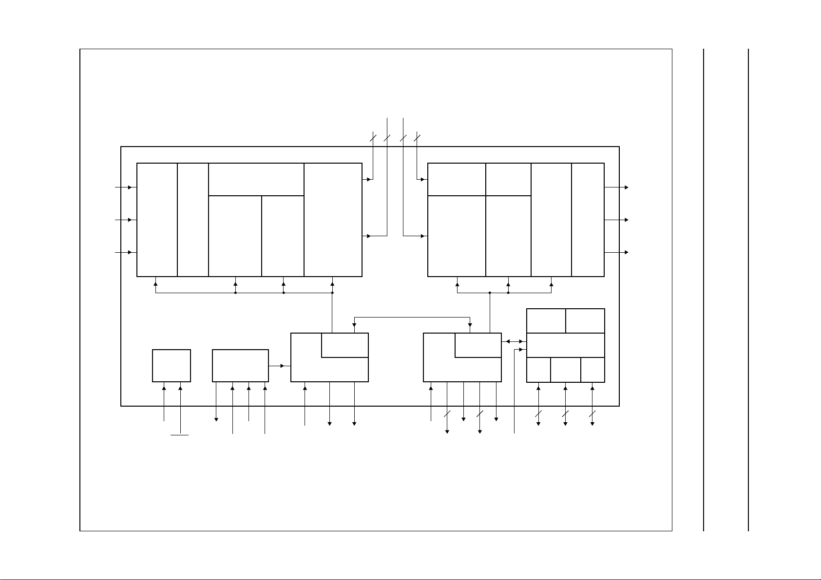
YIN
UIN
VIN
26
28
30
CLAMP
AGC
ANALOG
PREFILTER
TRIPLE
ADC
8 BIT
VARIABLE Y-DELAY
UV
CLAMP
CORRECTION
DOWN
SAMPLING
4 : 4 : 4
TO
4 : 1 : 1
HORIZONTAL
COMPRESSION
FORMATTER
dbook, full pagewidth
UVI7 to UVI4UVO7 to UVO4
YI7 to YI0YO7 to YO0
8 44 8
59
37
to
to
62
34
SAA4977H
51 to 5845 to 38
VARIABLE
Y-DELAY
REFORMATTER
SAMPLING
4 : 1 : 1
4 : 2 : 2
UP
TO
Y-PEAKING
DCTI
UP
SAMPLING
4 : 2 : 2
TO
4 : 4 : 4
BLANKING
SIDE-
PANELS
TRIPLE
DAC
10 BIT
79
76
74
YOUT
UOUT
VOUT
5 BLOCK DIAGRAM
Philips Semiconductors Preliminary specification
Besic SAA4977H
TEST
CONTROL
BLOCK
15
TMS
TRST
SNERT-
BUS
12,
13, 10
3
SNDA,
SNCL,
SNRST
RAM
BUS
SDA,
SCL
I2C-
1, 2
2
MGM592
ROM
(DISPLAY)
70
RE
IE2
CONTROL
INTERFACE
63,
64
66
2
BLND
HDFL
VDFL
71,
72
2
HRD
68 9
RST
MICROPROCESSOR
I/O
PORT
3 to 7
5
P1.5
to
P1.1
CONTROL
INTERFACE
ACQUISITION
PLL
47
33
LLA
22HA17
SELCLK
49
SWC
MEMORY CONTROL
(ACQUISITION)
32
20
RSTW
WE
VA
24
MEMORY CONTROL
LLD
Fig.1 Block diagram.
Philips Semiconductors Preliminary specification
Besic SAA4977H
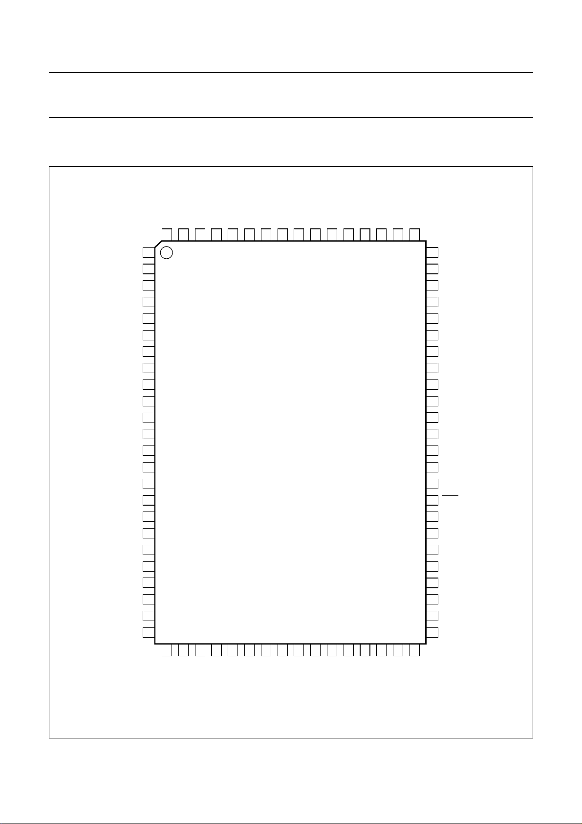
6 PINNING INFORMATION
6.1 Pinning
handbook, full pagewidth
SDA
SCL
P1.5
P1.4
P1.3
P1.2
P1.1
V
DDD5
RST
SNRST
V
DDD6
SNDA
SNCL
V
SSD4
TMS
V
SSD1
SELCLK
V
DDD1
V
DDD2
VA
V
SSA1
HA
V
DDA1
RSTW
DDA5
V
YOUT
80
79
1
2
3
4
5
6
7
8
9
10
11
12
13
14
15
16
17
18
19
20
21
22
23
24
SSA6
V
78
SSA5
V
77
UOUT
76
DDA4
V
75
SSA4
VOUT
V
74
73
SAA4977H
VDFL
72
HDFL
71
LLD
70
DDD4
V
69
HRD
68
DDIO
V
67
BLND
66
SSIO
V
65
IE2
64
RE
63
UVI4
62
UVI5
61
UVI6
60
UVI7
59
YI0
58
YI1
57
YI2
56
YI3
55
YI4
54
YI5
53
YI6
52
YI7
51
V
50
SSD3
TRST
49
V
48
SSD2
SWC
47
V
46
DDD3
YO7
45
YO6
44
YO5
43
YO4
42
YO3
41
25
26
27
28
29
30
31
32
DDA2
V
YIN
SSA2
V
UIN
DDA3
V
VIN
SSA3
V
WE
Fig.2 Pin configuration.
2000 May 25 5
33
LLA
34
UVO4
35
UVO5
36
UVO6
37
UVO7
38
YO0
39
YO1
40
YO2
MGM593

Philips Semiconductors Preliminary specification
Besic SAA4977H
6.2 Pin description Table 1 QFP80 package
SYMBOL PIN DESCRIPTION
2
SDA 1 I
SCL 2 I
P1.5 3 Port 1 data input/output signal 5
P1.4 4 Port 1 data input/output signal 4
P1.3 5 Port 1 data input/output signal 3
P1.2 6 Port 1 data input/output signal 2
P1.1 7 Port 1 data input/output signal 1
V
DDD5
8 digital supply voltage 5 (3.3 V)
RST 9 microprocessor reset input
SNRST 10 SNERT restart (port 1.0)
V
DDD6
11 digital supply voltage 6 (3.3 V)
SNDA 12 SNERT data
SNCL 13 SNERT clock
V
SSD4
14 digital ground 4
TMS 15 test mode select
V
SSD1
16 digital ground 1
SELCLK 17 select acquisition clock input; internal PLL if HIGH, external clock if LOW
V
V
DDD1
DDD2
18 digital supply voltage 1 (5 V)
19 digital supply voltage 2 (5 V)
VA 20 vertical synchronization input, acquisition part
V
SSA1
21 analog ground 1
HA 22 analog/digital horizontal reference input
V
DDA1
23 analog supply voltage 1 (5 V)
RSTW 24 reset write signal output, memory 1
V
DDA2
25 analog supply voltage 2 (5 V)
YIN 26 Y analog input
V
SSA2
27 analog ground 2
UIN 28 U analog input
V
DDA3
29 analog supply voltage 3 (5 V)
VIN 30 V analog input
V
SSA3
31 analog ground 3
WE 32 write enable signal output, memory 1
LLA 33 acquisition clock input
UVO4 34 V digital output bit 0
UVO5 35 V digital output bit 1
UVO6 36 U digital output bit 0
UVO7 37 U digital output bit 1
YO0 38 Y digital output bit 0
C-bus serial data (P1.7)
2
C-bus serial clock (P1.6)
2000 May 25 6
Philips Semiconductors Preliminary specification
Besic SAA4977H
SYMBOL PIN DESCRIPTION
YO1 39 Y digital output bit 1
YO2 40 Y digital output bit 2
YO3 41 Y digital output bit 3
YO4 42 Y digital output bit 4
YO5 43 Y digital output bit 5
YO6 44 Y digital output bit 6
YO7 45 Y digital output bit 7 (MSB)
V
DDD3
SWC 47 serial write clock output
V
SSD2
TRST 49 test reset, active LOW
V
SSD3
YI7 51 Y digital input bit 7 (MSB)
YI6 52 Y digital input bit 6
YI5 53 Y digital input bit 5
YI4 54 Y digital input bit 4
YI3 55 Y digital input bit 3
YI2 56 Y digital input bit 2
YI1 57 Y digital input bit 1
YI0 58 Y digital input bit 0
UVI7 59 U digital input bit 1
UVI6 60 U digital input bit 0
UVI5 61 V digital input bit 1
UVI4 62 V digital input bit 0
RE 63 read enable signal output, memory 1
IE2 64 input enable signal output, memory 2
V
SSIO
BLND 66 horizontal blanking signal output, display part
V
DDIO
HRD 68 horizontal reference signal output, deflection part
V
DDD4
LLD 70 display clock input
HDFL 71 horizontal synchronization signal output, deflection part
VDFL 72 vertical synchronization signal output, deflection part
V
SSA4
VOUT 74 V analog output
V
DDA4
UOUT 76 U analog output
V
SSA5
46 digital supply voltage 3 (5 V)
48 digital ground 2
50 digital ground 3
65 I/O ground
67 I/O supply voltage (5 V)
69 digital supply voltage 4 (3.3 V)
73 analog ground 4
75 analog supply voltage 4 (3.3 V)
77 analog ground 5
2000 May 25 7

Philips Semiconductors Preliminary specification
Besic SAA4977H
SYMBOL PIN DESCRIPTION
V
SSA6
YOUT 79 Y analog output
V
DDA5
78 analog ground 6
80 analog supply voltage 5 (3.3 V)
7 FUNCTIONAL DESCRIPTION
7.1 Analog-to-digital conversion
7.1.1 CLAMP CIRCUIT, CLAMPING Y TO DIGITAL LEVEL 16
AND UV TO 0 (2’S COMPLEMENT)
A clamp circuit is applied for each input channel, to map
the colourless black level in each video line (on the sync
back porch) to level 16 for Y and to the centre level of the
converters for U and V. During the clamp period, an
internally generated clamp pulse is used to switch on the
clamp action. An operational transconductance amplifier
like construction, which references to voltage reference
points in the ladders of the ADCs, will provide a current on
the input of the YUV signals, in order to bring the signals
to the correct DC value. This current is proportional to the
DC error, but is limited to ±100 µA. When the clamping
action is off, the residual clamp current should be very low
in order not to drift away within a video line.
7.1.2 GAIN ELEMENTS FOR AUTOMATIC GAIN CONTROL
A variable amplifier is used to map the possible YUV input
range to the ADC range. A rise of 6 dB up to a drop fall of
6 dB w.r.t. the nominal values can be achieved. The gain
setting within this range is done digitally via control
registers. For this purpose a gain setting DAC is
incorporated. The smallest step in the gain setting should
be hardly visible on the picture, which can be met with
smallest steps of 0.4%/step.
Luminance and chrominance gain settings can be
separately controlled. The reason for this split is that
U and V may be gain adjusted already, whereas
luminance is to be adjusted by the SAA4977H AGC. On
the other hand, for RGB originated sources, Y, U and V
should be adjusted with the same AGC gain.
7.1.3 ANALOG ANTI-ALIASING PREFILTERING
A third order linear phase filter is applied on each of the Y,
U and V channels. It provides a notch on f
(16 MHz) to
CLK
strongly prevent aliasing to low frequencies, which would
be the most disturbing. The bandwidth of the filters is
designed for −3 dB at 5.6 MHz. The filters can be
bypassed if external filtering with other characteristics is
desired.
7.1.4 TRIPLE 8-BIT ANALOG-TO-DIGITAL CONVERSION
Three identical ADCs are used to convert Y, U and V with
16 MHz data rate. A multi-step type ADC is applied here.
7.2 Digital processing at 1fH level
7.2.1 O
VERLOAD DETECTION
The overload detection provides information to make
efficient use of the AGC. The number of overflows per
video field in the luminance channel is accumulated by a
14-bitcounter. The 8 MSBs of this counter can beread out
by the microprocessor respectively via the I2C-bus.
Overflow levels can be programmed as 216, 224,
232 and 240.
7.2.2 D
IGITAL CLAMP CORRECTION FOR UV
During 32 samples within the clamp position the clamp
error is measured and accumulated to make a low-pass
filtered value of the clamp error. Then a vertical recursive
filter is used to further low-pass this error value. This value
can be read by the microprocessor or directly be used to
correct the clamp error. It is also possible to give a fixed
correction value by the microprocessor.
7.2.3 4:4:4TO 4:1:1DOWN-SAMPLING AND UV
CORING
The U and V samples from the ADC are low-pass filtered,
before being subsampled with a factor of 2. Coring is
applied to the subsampled signal to obtain no gain for low
amplitudes which is considered to be noise. Coring levels
can be programmed as 0 (off), ±1⁄2, ±1 and ±2 LSB.
The U and V samples from the 4:2:2data are low-pass
filtered again, before being subsampled a second time
with a factor of 2 and formatted to 4 :1:1 format.
7.2.4 Y-DELAY
The Y samples can be shifted onto 8 positions w.r.t. the
UV samples. This shift is meant to account for a possible
difference in delay previous to the SAA4977H. The zero
delay setting is suitable for the nominal case of aligned
input data according to the interface format standard.
Theothersettingsprovide four samples less delay to three
sample more delay in Y.
2000 May 25 8

Philips Semiconductors Preliminary specification
Besic SAA4977H
7.2.5 HORIZONTAL COMPRESSION
For displaying 4 : 3 sources on 16 : 9 screens a horizontal
signal compression can be done by data interpolation.
Therefore two horizontal compression factors of either
4
⁄3or7⁄6arepossible.ViatheI2C-busthecompressioncan
be switched on or off and the compression mode 16 : 9 or
14 : 9 can be selected. When the compression mode is
active, a reduced number of the interpolated data is stored
in the field memory. To achieve sufficiently high accuracy
in interpolation Variable Phase Delay filters are used
(VPD10 for luminance, a multiplexed VPD06 for UV).
7.3 Digital processing at 2fH level
7.3.1 4:1:1
TO 4:2:2UP-CONVERSION
An up-converter to 4:2:2 is applied with a linear
interpolation filter for creation of the extra samples. These
are combined with the original samples from the 4 :1:1
stream.
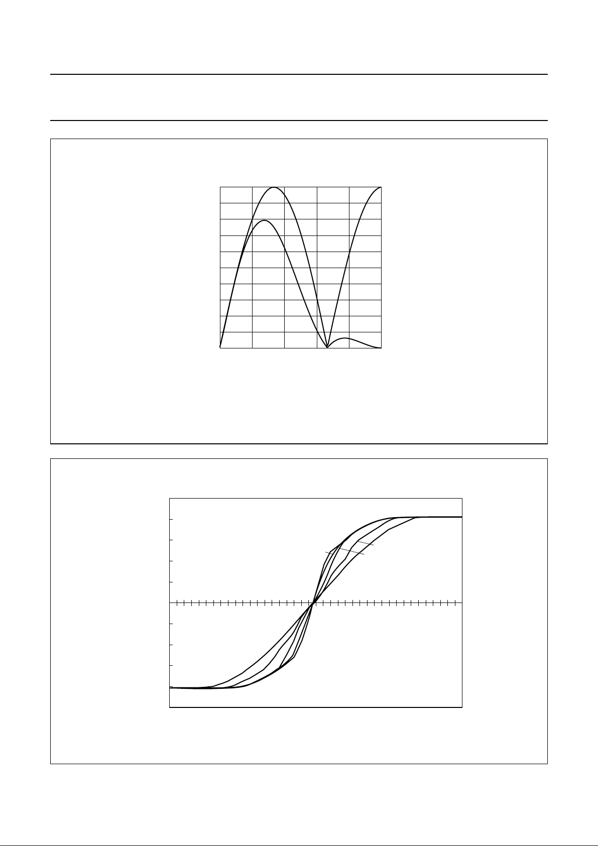
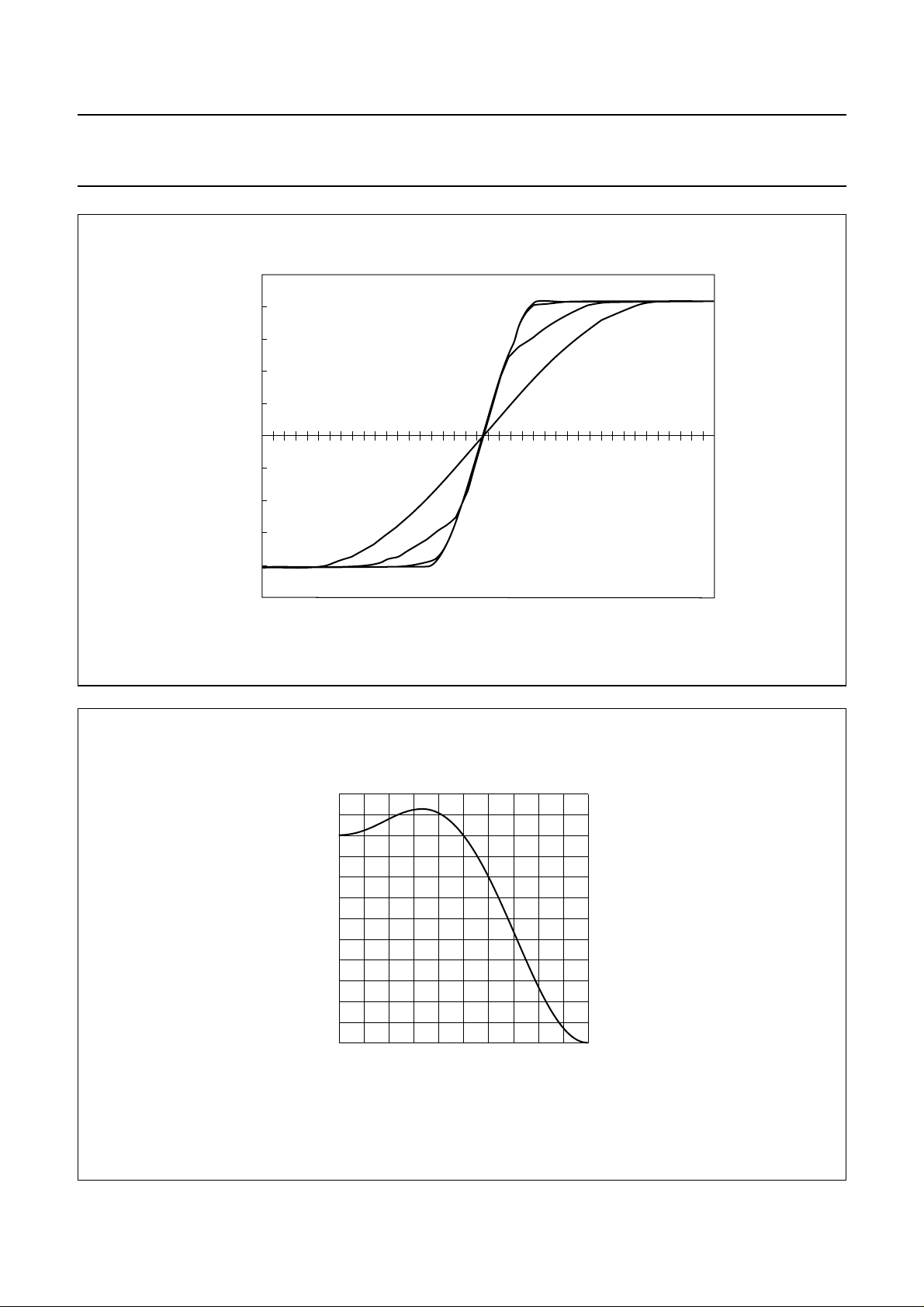
7.3.2 DCTI
The Digital Colour Transient Improvement (DCTI) is
intended for U and V signals originating from a 4 :1:1
source. Horizontal transients are detected and enhanced
without overshoots by differentiating, make absolute and
again differentiating the U and V signals separately.
This results in a 4:4:4 U and V bandwidth. To prevent
third harmonic distortion, typical for this processing, a so
called over the hill protection prevents peak signals
becoming distorted. Via the I2C-bus it is possible to
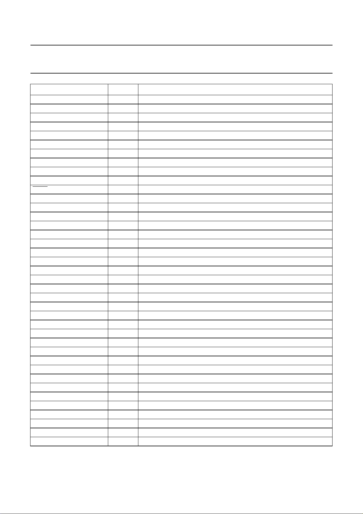
control: gain width (see Fig.4), threshold (i.e. immunity
against noise), selection of simple or improved first
differentiating filter (see Fig.3), limit for pixel shift range
(see Fig.5), common or separate processing of U and V
signals, hill protection mode (i.e. no discolourations in
narrow colour gaps), low-pass filtering for U and V signals
(see Fig.6) and a so called super hill mode, which avoids
discolourations in transients within a colour component.
7.3.3 Y-PEAKING
A linear peaking is applied, which amplifies the luminance
signal in the middle and the upper ranges of the
bandwidth.
The filtering is an addition of:
• The original signal
• The original signal high-passed with maximum gain at
frequency =1⁄2fs (8 MHz)
• The original signal band-passed with centre
frequency =1⁄4fs (4 MHz)
• The original signal band-passed with centre frequency
of 2.38 MHz.
The band-passed and high-passed signals are weighted
1
with factors 0,
⁄16,2⁄16,3⁄16,4⁄16,5⁄16,6⁄16, and8⁄16, resulting
in a maximum gain difference of 2 dB at the centre
frequencies.
Coring is added to obtain no gain for low amplitudes in the
high-pass and band-pass filtered signal, which is
considered to be noise. Coring levels can be programmed
as 0 (off), ±8, ±16, ±24 to ±120 LSB w.r.t. the (signed)
11-bit filtered signal.
In addition the peaking gain can be reduced depending on
the signal amplitude, programming range 0 (no
attenuation),1⁄4,2⁄4, and4⁄4. It is also possible to make
largerundershootsthanovershoots,programmingrange 0
(no attenuation of undershoots),1⁄4,2⁄4, and4⁄4.
7.3.4 Y-DELAY
The Y samples can be shifted onto 8 positions w.r.t. the
UV samples. This shift is meant to account for a possible
difference in delay previous to the SAA4977H. The zero
delay setting is suitable for the nominal case of aligned
input data. The other settings provide one to seven
samples less delay in Y.
7.3.5 SIDEPANELS AND BLANKING
Sidepanels are generated by switching Y and the 4 MSBs
of U and V to certain programmable values. The start and
stop values for the sidepanels w.r.t. the rising edge of the
HRD signal are programmable in a resolution of 4 LLD
clock cycles. In addition, a fine shift of 0 to 3 LLD clock
cycles of both values can be achieved.
Blanking is done by switching Y to value 64 at 10-bit word
and UV to value 0 (in 2’s complement). Blanking is
controlled by a composite signal HVBDA, consisting of a
horizontal part HBDA and a vertical part VBDA. Set and
reset value of the horizontal control signal HBDA are
programmable w.r.t. the rising edge of the HRD signal, set
and reset value of the vertical control signal VBDA are
programmable w.r.t. the rising edge of the VA signal.
The range of the Y output signal can be selected between
9 and 10 bits. In the case of 9 bits for the nominal signal
there is room left for undershoot and overshoot (adding up
to a total of 10 bits). In the case of selecting all 10 bits of
the luminance DAC for the nominal signal any under or
overshoot will be clipped (see Fig.11).
2000 May 25 9
Philips Semiconductors Preliminary specification
Besic SAA4977H
(1) dcti_ddx_sel = 1.
(2) dcti_ddx_sel = 0.
Fig.3 DCTI first differentiating filter; transfer function with variation of control signal dcti_ddx_sel.
signal
amplitude
0.8
0.6
0.4
0.2
1
0
0 0.25
handbook, halfpage
(2)(1)
0.05 0.1 0.15 0.2
MGM689
f/f
s
handbook, full pagewidth
amplitude
(1) input signal.
(2) gain = 1.
(3) gain = 3.
(4) gain = 5.
(5) gain = 7.
digital
signal
500
400
300
200
100
0
−100
−200
−300
−400
−500
Fig.4 DCTI with variation of gain setting (limit = 1).
2000 May 25 10
MGM690
(1)
(4)
(5)
(2)
(3)
samples
Philips Semiconductors Preliminary specification
Besic SAA4977H
handbook, full pagewidth
(1) input signal.
(2) limit = 1.
(3) limit = 2.
(4) limit = 3.
digital
signal
amplitude
500
400
300
200
100
−100
−200
−300
−400
−500
MGM691
(4)
(3)
(2)
(1)
0
samples
Fig.5 DCTI with variation of limit setting (gain = 7).
1.2
handbook, halfpage
signal
amplitude
0.8
0.4
0
0 0.5
0.1 0.2 0.3 0.4
Fig.6 DCTI post-filter transfer function.
2000 May 25 11
MGM692
f/f
s
 Loading...