

Philips SAA4974H Datasheet
INTEGRATED CIRCUITS
DATA SH EET
SAA4974H
Besic without ADC
Product specification
File under Integrated Circuits, IC02
1998 Apr 21

Philips Semiconductors Product specification
Besic without ADC SAA4974H
CONTENTS
1 FEATURES
2 GENERAL DESCRIPTION
3 QUICK REFERENCE DATA
4 ORDERING INFORMATION
5 BLOCK DIAGRAM
6 PINNING INFORMATION
6.1 Pinning
6.2 Pin description
7 FUNCTIONAL DESCRIPTION
7.1 Digital processing at 2fH level
7.1.1 4:1:1 to 4:2:2 up-conversion
7.1.2 DCTI
7.1.3 Y-peaking
7.1.4 Y-delay
7.1.5 Sidepanels and blanking
7.2 Digital-to-analog conversion
7.3 Microprocessor
7.3.1 I2C-bus
7.3.2 SNERT-bus
7.3.3 I/O-ports
7.3.4 Watchdog timer
7.4 Memory controller
7.4.1 WE
7.4.2 RSTW
7.4.3 RE
7.4.4 IE2
7.4.5 HDFL
7.4.6 VDFL
7.4.7 BLND
7.5 Clock and sync interfacing
7.6 4:1:1 digital input interfacing
7.7 Test mode operation
7.8 I2C-bus control registers
8 LIMITING VALUES
9 THERMAL CHARACTERISTICS
10 CHARACTERISTICS
11 APPLICATION
12 PACKAGE OUTLINE
13 SOLDERING
13.1 Introduction
13.2 Reflow soldering
13.3 Wave soldering
13.4 Repairing soldered joints
14 DEFINITIONS
15 LIFE SUPPORT APPLICATIONS
16 PURCHASE OF PHILIPS I2C COMPONENTS
1998 Apr 21 2
Philips Semiconductors Product specification
Besic without ADC SAA4974H
1 FEATURES
• Field rate up-conversion (50 to 100 Hz or 60 to 120 Hz)
• 4:1:1 digital input
• Digital Colour Transient Improvement (DCTI)
• Digital luminance peaking
• Triple 10-bit Digital-to-Analog Converter (DAC)
• Memory controller
• Embedded microprocessor
• 16 kbyte ROM
• 256 byte RAM
2
C-bus interface
• I
• Synchronous No parity Eight bit Reception and
Transmission (SNERT) interface.
2 GENERAL DESCRIPTION
The SAA4974H is a video processing IC providing a digital
YUV 4:1:1 input interface, analog YUV output, video
enhancing features, memory controlling and an embedded
80C51 microprocessor core. It is applicable especially for
field rate up-conversion (50 to 100 Hz or 60 to 120 Hz) in
cooperation with a 2.9 Mbit field memory. It is designed for
applications together with:
SAA7111A, VPC3200 (video decoder)
SAA4955/56TJ, TMS4C2972/73 (serial field memories)
SAA4990H (PROZONIC)
SAA4991WP (MELZONIC).
3 QUICK REFERENCE DATA
SYMBOL PARAMETER MIN. TYP. MAX. UNIT
V
DDA(1,2)
V
DDD(1,2,3)
V
DDIO(1,2,3)
I
DDA(1,2)
I
DDD(1,2,3)
I
DDIO(1,2,3)
P
tot
T
amb
analog supply voltage 3.15 3.3 3.45 V
digital supply voltage 3.0 3.3 3.6 V
I/O supply voltage 4.5 5.0 5.5 V
analog supply current − 25 40 mA
digital supply current − 50 70 mA
I/O supply current − 10 20 mA
total power dissipation −−0.5 W
operating ambient temperature −20 − +70 °C
4 ORDERING INFORMATION
PACKAGE
TYPE NUMBER
NAME DESCRIPTION VERSION
SAA4974H QFP80 plastic quad flat package; 80 leads (lead length 1.95 mm);
body 14 × 20 × 2.8 mm
SOT318-2
1998 Apr 21 3
This text is here in white to force landscape pages to be rotated correctly when browsing through the pdf in the Acrobat reader.This text is here in
o
_white to force landscape pages to be rotated correctly when browsing through the pdf in the Acrobat reader.This text is here inThis text is here in
white to force landscape pages to be rotated correctly when browsing through the pdf in the Acrobat reader. white to force landscape pages to be ...
1998 Apr 21 4
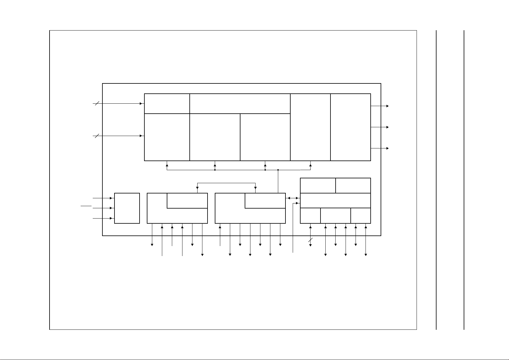
8
YI7 to YI0
51 to 58
VARIABLE
Y-DELAY
ok, full pagewidth
Y-PEAKING
79
BLANKING
YOUT
5 BLOCK DIAGRAM
Besic without ADC SAA4974H
Philips Semiconductors Product specification
UVI7 to UVI4
TMS
TRST
ANATEST
4
59 to 62
15
49
30
SAA4974H
TEST
CONTROL
BLOCK
REFORMATTER
MEMORY CONTROL
(ACQUISITION)
47
33
SWC
LLA
CONTROL
INTERFACE
22HA20
WE
VA
UP-CONVERSION
4 : 1 : 1
TO
4 : 2 : 2
70
24
32
LLD
RSTW
DCTI
UP-CONVERSION
4 : 2 : 2
TO
4 : 4 : 4
CONTROL
INTERFACE
MEMORY CONTROL
(DISPLAY)
71
IE2
BLND
66
HDFL
VDFL
63RE64
72
HRD
68 9
RST
SIDEPANELS
OVERLAY
ROM
MICROPROCESSOR
I/O
PORT
3 to 7
5
P1.5
to
P1.1
SNDA
SNERT-
BUS
13
12
SNCL
TRIPLE
10-BIT DAC
RAM
10 2
SDA
SNRST
I2C-
BUS
1
SCL
76
UOUT
74
VOUT
MGM687
Fig.1 Block diagram.
Philips Semiconductors Product specification
Besic without ADC SAA4974H
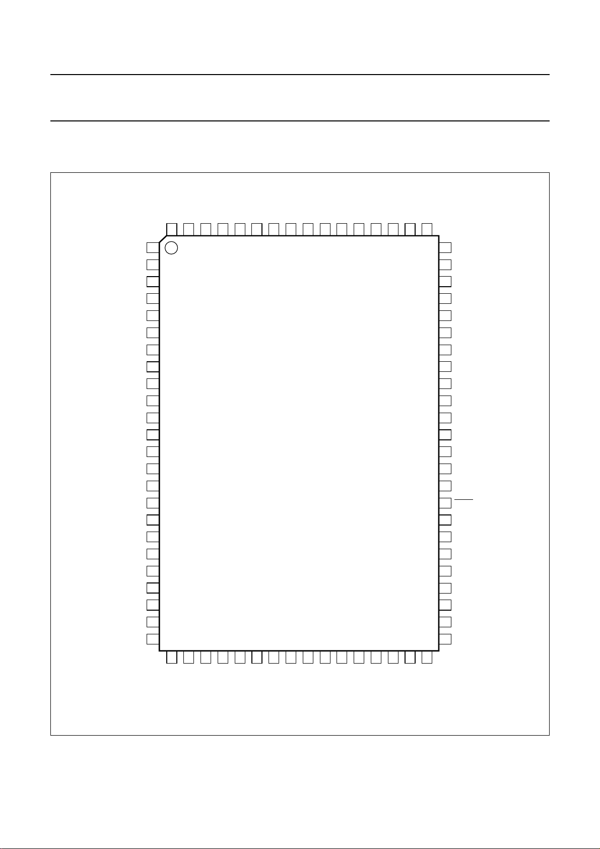
6 PINNING INFORMATION
6.1 Pinning
handbook, full pagewidth
SDA
SCL
P1.5
P1.4
P1.3
P1.2
P1.1
V
DDD1
RST
SNRST
V
DDD2
SNDA
SNCL
V
SSD1
TMS
V
SSIO1
V
DDIO1
V
SSD2
RSTW
n.c.
n.c.
VA
HA
n.c.
DDA2
V
YOUT
80
79
1
2
3
4
5
6
7
8
9
10
11
12
13
14
15
16
17
18
19
20
21
22
23
24
SSA3
V
78
SSA2
V
77
UOUT
76
DDA1
V
75
SSA1
VOUT
V
74
73
SAA4974H
VDFL
72
HDFL
71
LLD
70
DDD3
V
69
HRD
68
DDIO3
V
67
BLND
66
SSIO3
V
65
IE2
64
RE
63
UVI4
62
UVI5
61
UVI6
60
UVI7
59
YI0
58
YI1
57
YI2
56
YI3
55
YI4
54
YI5
53
YI6
52
YI7
51
V
50
SSD3
49
TRST
V
48
SSIO2
SWC
47
V
46
DDIO2
n.c.
45
n.c.
44
n.c.
43
n.c.
42
n.c.
41
25
n.c.
26
n.c.
27
n.c.
28
n.c.
29
n.c.
30
ANATEST
31
n.c.
32
WE
Fig.2 Pin configuration.
1998 Apr 21 5
33
LLA
34
n.c.
35
n.c.
36
n.c.
37
n.c.
38
n.c.
39
n.c.
40
n.c.
MGM688

Philips Semiconductors Product specification
Besic without ADC SAA4974H
6.2 Pin description Table 1 SOT318-2 package
SYMBOL PIN DESCRIPTION
SDA 1 I
SCL 2 I
P1.5 3 Port 1 data input/output signal 5
P1.4 4 Port 1 data input/output signal 4
P1.3 5 Port 1 data input/output signal 3
P1.2 6 Port 1 data input/output signal 2
P1.1 7 Port 1 data input/output signal 1
V
DDD1
8 digital supply voltage 1 (3.3 V)
RST 9 microprocessor reset input
SNRST 10 SNERT restart (port 1.0)
V
DDD2
11 digital supply voltage 2 (3.3 V)
SNDA 12 SNERT data
SNCL 13 SNERT clock
V
SSD1
14 digital ground 1
TMS 15 test mode select
V
SSIO1
16 I/O ground 1
n.c. 17 not connected
V
DDIO1
18 I/O supply voltage 1 (5 V)
n.c. 19 not connected
VA 20 vertical synchronization input, acquisition part
V
SSD2
21 digital ground 2
HA 22 digital horizontal reference input
n.c. 23 not connected
RSTW 24 reset write signal output, memory 1
n.c. 25 not connected
n.c. 26 not connected
n.c. 27 not connected
n.c. 28 not connected
n.c. 29 not connected
ANATEST 30 analog test input
n.c. 31 not connected
WE 32 write enable signal output, memory 1
LLA 33 acquisition clock input
n.c. 34 not connected
n.c. 35 not connected
n.c. 36 not connected
n.c. 37 not connected
n.c. 38 not connected
2
C-bus serial data (P 1.7)
2
C-bus serial clock (P 1.6)
1998 Apr 21 6

Philips Semiconductors Product specification
Besic without ADC SAA4974H
SYMBOL PIN DESCRIPTION
n.c. 39 not connected
n.c. 40 not connected
n.c. 41 not connected
n.c. 42 not connected
n.c. 43 not connected
n.c. 44 not connected
n.c. 45 not connected
V
DDIO2
SWC 47 serial write clock output
V
SSIO2
TRST 49 test reset, LOW active
V
SSD3
YI7 51 Y digital input bit 7 (MSB)
YI6 52 Y digital input bit 6
YI5 53 Y digital input bit 5
YI4 54 Y digital input bit 4
YI3 55 Y digital input bit 3
YI2 56 Y digital input bit 2
YI1 57 Y digital input bit 1
YI0 58 Y digital input bit 0
UVI7 59 U digital input bit 1
UVI6 60 U digital input bit 0
UVI5 61 V digital input bit 1
UVI4 62 V digital input bit 0
RE 63 read enable signal output, memory 1
IE2 64 input enable signal output, memory 2
V
SSIO3
BLND 66 horizontal blanking signal output, display part
V
DDIO3
HRD 68 horizontal reference signal output, deflection part
V
DDD3
LLD 70 display clock input
HDFL 71 horizontal synchronization signal output, deflection part
VDFL 72 vertical synchronization signal output, deflection part
V
SSA1
VOUT 74 V analog output
V
DDA1
UOUT 76 U analog output
V
SSA2
46 I/O supply voltage 2 (5 V)
48 I/O ground 2
50 digital ground 3
65 I/O ground 3
67 I/O supply voltage 3 (5 V)
69 digital supply voltage 3 (3.3 V)
73 analog ground 1
75 analog supply voltage 1 (3.3 V)
77 analog ground 2
1998 Apr 21 7

Philips Semiconductors Product specification
Besic without ADC SAA4974H
SYMBOL PIN DESCRIPTION
V
SSA3
YOUT 79 Y analog output
V
DDA2
7 FUNCTIONAL DESCRIPTION
7.1 Digital processing at 2f
7.1.1 4:1:1
An up-converter to 4:2:2 is applied with a linear
interpolation filter for creation of the extra samples. These
are combined with the original samples from the 4 :1:1
stream.
7.1.2 DCTI
The Digital Colour Transient Improvement (DCTI) is
intended for U and V signals originating from a 4:1:1
source. Horizontal transients are detected and enhanced
without overshoots by differentiating, make absolute and
again differentiating the U and V signals separately. This
results in a 4:4:4 UandV bandwidth. To prevent third
harmonic distortion, typical for this processing, a so called
over the hill protection prevents peak signals to become
distorted.
78 analog ground 3
80 analog supply voltage 2 (3.3 V)
level
H
TO 4:2:2UP-CONVERSION
2
Via I
C-bus it is possible to control: gain width (see Fig.4),
threshold (i.e. immunity against noise), selection of simple
or improved first differentiating filter (see Fig.3), limit for
pixel shift range (see Fig.5), common or separate
processing of U and V signals, hill protection mode (i.e. no
discolourations in narrow colour gaps), low-pass filtering
for U and V signals (see Fig.6) and a so called super hill
mode, which avoids discolourations in transients within a
colour component.
1998 Apr 21 8
Philips Semiconductors Product specification
Besic without ADC SAA4974H
(1) dcti_ddx_sel = 1.
(2) dcti_ddx_sel = 0.
Fig.3 DCTI first differentiating filter; transfer function with variation of control signal dcti_ddx_sel.
signal
amplitude
0.8
0.6
0.4
0.2
1
0
0 0.25
handbook, halfpage
(2)(1)
0.05 0.1 0.15 0.2
MGM689
f/f
s
handbook, full pagewidth
(1) Input signal.
(2) Gain = 1.
(3) Gain = 3.
(4) Gain = 5.
(5) Gain = 7.
digital
signal
amplitude
500
400
300
200
100
−100
−200
−300
−400
−500
MGM690
(1)
(4)
(5)
0
(2)
(3)
samples
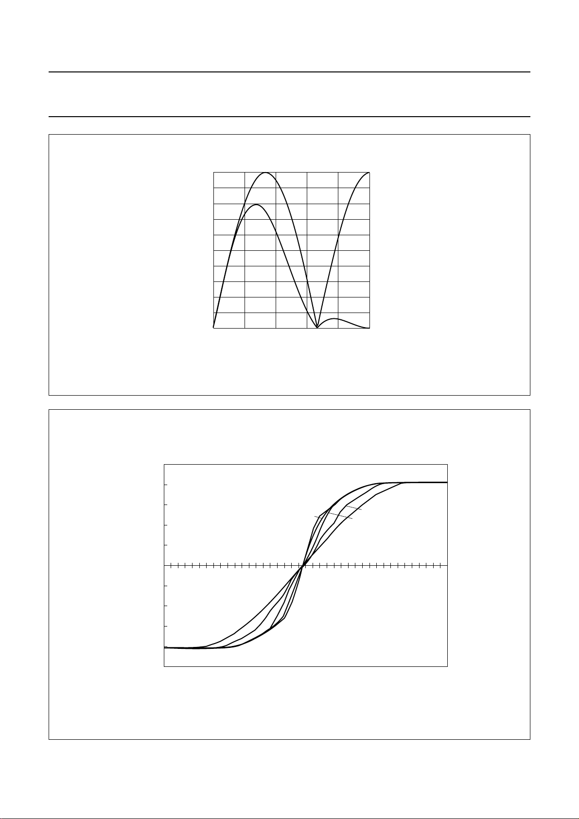
Fig.4 DCTI with variation of gain setting (limit = 1).
1998 Apr 21 9
 Loading...