

Philips saa4970t DATASHEETS

INTEGRATED CIRCUITS
DATA SH EET
SAA4970T
Economical video processing IC
(ECOBENDIC)
Preliminary specification
File under Integrated Circuits, IC02
1996 Oct 25

Philips Semiconductors Preliminary specification
Economical video processing IC
SAA4970T
(ECOBENDIC)
FEATURES
• Digital horizontal PLL
• Digital CTI (DCTI)
• Digital luminance peaking
• Digital phase compensation filter
• D/A conversion
• Simple multi picture processing
• Coloured frame generation
• Memory/sync processing.
QUICK REFERENCE DATA
SYMBOL PARAMETER MIN. MAX. UNIT
V
DD
V
CC
T
amb
digital supply voltage 4.5 5.5 V
analog supply voltage 4.75 5.25 V
operating ambient temperature 0 70 °C
GENERAL DESCRIPTION
The ECOBENDIC is an economical video processing IC
(Economical Back End IC) for double scan conversion.
It consists of sync/memory control, video enhancing
features and D/A conversion. The IC is designed to
cooperate with an 83C654 type of microcontroller,
Texas Instruments TMS4C2970/2971 memories plus a
4:1:1 A/D converter TDA8755/8753A.
ORDERING INFORMATION
TYPE NUMBER
NAME DESCRIPTION VERSION
SAA4970T VSO56 plastic very small outline package; 56 leads SOT190-1
PACKAGE
1996 Oct 25 2
Philips Semiconductors Preliminary specification
Economical video processing IC
(ECOBENDIC)
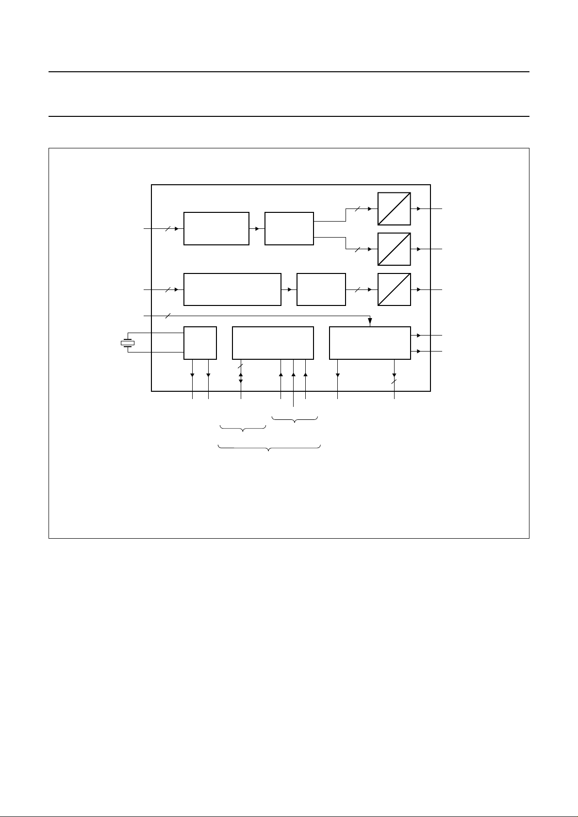
BLOCK DIAGRAM
handbook, full pagewidth
47 to
UVIN3
to UVIN0
YIN7
to YIN0
HA, V
Xtal
Xtal
A
O
I
50
37 to 41,
44 to 46
22, 23
55
56
REFORMATTER
UP-SAMPLING
4
PHASE COMPENSATION
PLL
53
FILTER
51
8
2
CK1 CK2 ALE
SAA4970T
MICROCONTROLLER
INTERFACE
8
29 to 36
parallel bus
AD7 to AD0
address line
microcontroller
DCTI
24 27 28
RDN CLMP IE, WE, REmicrocontroller
WRN
command
PEAKING
8
8
9
SYNC PROCESSING
MEMORY CONTROL
14
D
D
D
3
A
A
A
15 to 17
SAA4970T
3
U
O
5
V
O
7
Y
O
19
H
D
18
V
D
MGE092
microcontroller parallel bits
Fig.1 Block diagram.
1996 Oct 25 3

Philips Semiconductors Preliminary specification
Economical video processing IC
SAA4970T
(ECOBENDIC)
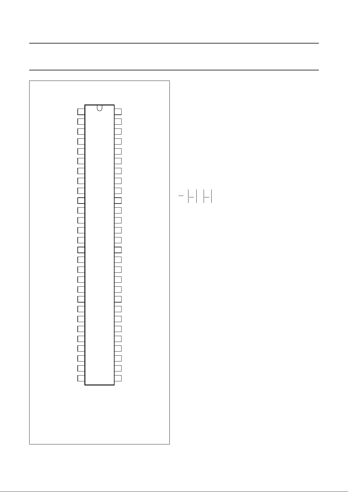
PINNING
SYMBOL PIN TYPE DESCRIPTION
TEST2 1 input test control
P
mirref
U
O
V
SSA
V
O
V
CC
Y
O
V
ref
I
ref
V
refH
R1 11 I/O reset acquisition horizontal counter
R2 12 I/O reset display horizontal counter
PIP 13 input PIP related input 0
CLMP 14 output clamping control
IE 15 output field memory input enable
WE 16 output field memory write enable
RE 17 output field memory read enable
V
D
H
D
RESET 20 output watchdog output (microcontroller reset)
BONE 21 input watchdog input (microcontroller bone)
H
A
V
A
ALE 24 input address latch enable
IT1 25 output acquisition related interrupt
IT2 26 output display related interrupt
WRN 27 input write not pulse
RDN 28 input read not pulse
AD7 29 I/O programmable signal positioner (psp) data bus bit 7 (MSB)
AD6 30 I/O psp data bus bit 6
AD5 31 I/O psp data bus bit 5
AD4 32 I/O psp data bus bit 4
AD3 33 I/O psp data bus bit 3
AD2 34 I/O psp data bus bit 2
AD1 35 I/O psp data bus bit 1
AD0 36 I/O psp data bus bit 0 (LSB)
YIN7 37 input Y input bus bit 7 (MSB)
YIN6 38 input Y input bus bit 6
YIN5 39 input Y input bus bit 5
YIN4 40 input Y input bus bit 4
2 input decoupling P-mirror reference
3 output analog U output
4 ground analog ground (0 V)
5 output analog V output
6 supply analog supply voltage (+5 V)
7 output analog Y output
8 supply analog supply voltage reference D/A ladder HIGH
9 supply reference current
10 supply D/A decoupling capacitor
18 I/O display vertical pulse
19 output display horizontal pulse
22 I/O acquisition horizontal pulse
23 I/O acquisition vertical pulse
1996 Oct 25 4

Philips Semiconductors Preliminary specification
Economical video processing IC
(ECOBENDIC)
SYMBOL PIN TYPE DESCRIPTION
YIN3 41 input Y input bus bit 3
V
DD
V
SS
YIN2 44 input Y input bus bit 2
YIN1 45 input Y input bus bit 1
YIN0 46 input Y input bus bit 0 (LSB)
UVIN3 47 input UV input bus bit 3 (MSB)
UVIN2 48 input UV input bus bit 2
UVIN1 49 input UV input bus bit 1
UVIN0 50 input UV input bus bit 0 (LSB)
CK2 51 I/O display clock
V
SS
CK1 53 I/O acquisition clock
TEST1 54 input test control
Xtal
O
Xtal
I
42 supply digital supply voltage (+5 V)
43 ground digital ground (0 V)
52 ground digital ground (0 V)
55 output external crystal output (12 MHz)
56 input PLL crystal input (12 MHz)
SAA4970T
1996 Oct 25 5
Philips Semiconductors Preliminary specification
Economical video processing IC
(ECOBENDIC)
handbook, halfpage
TEST2
P
mirref
U
V
SSA
V
V
CC
Y
V
ref
I
ref
V
refH
R1
R2
PIP
CLMP
WE
RE
V
H
RESET
BONE
H
V
ALE
IT1
IT2
WRN
RDN
O
O
O
IE
D
D
A
A
1
2
3
4
5
6
7
8
9
10
11
12
13
14
SAA4970T
15
16
17
18
19
20
21
22
23
24
25
26
27
28
MGE091
Xtal
56
I
Xtal
55
O
TEST1
54
CK1
53
V
52
SS
CK2
51
UVIN0
50
UVIN1
49
UVIN2
48
UVIN3
47
YIN0
46
YIN1
45
YIN2
44
V
43
SS
V
42
DD
YIN3
41
YIN4
40
YIN5
39
YIN6
38
YIN7
37
AD0
36
AD1
35
AD2
34
AD3
33
AD4
32
AD5
31
AD6
30
AD7
29
SAA4970T
FUNCTIONAL DESCRIPTION
ECO data path
The data path performs the DCTI, peaking, phase
compensation, framing and blanking functions plus colour
reformatting and variable delay of Y to UV at the input and
output of the data path.
DCTI
DCTI is implemented to get a dynamic interpolation of the
low bandwidth U and V signals. First a 2 : 1 linear
interpolation is done, to go from a 4 :1:1 format to a
4:2:2 format. A second interpolation is done in which the
data path delay is varied on the basis of a function of the
second derivative of the U and V signal (or more precise:
d
dUtddV
+{}
td
td
first half the data path delay is higher than nominal and in
the second half it is lower than nominal. This will make the
edge much steeper. As this second interpolation is done
with the resolution equal to that of the Y samples and also
with a zero DCTI gain a 2 : 1 interpolation is performed, a
4:4:4 format is obtained.
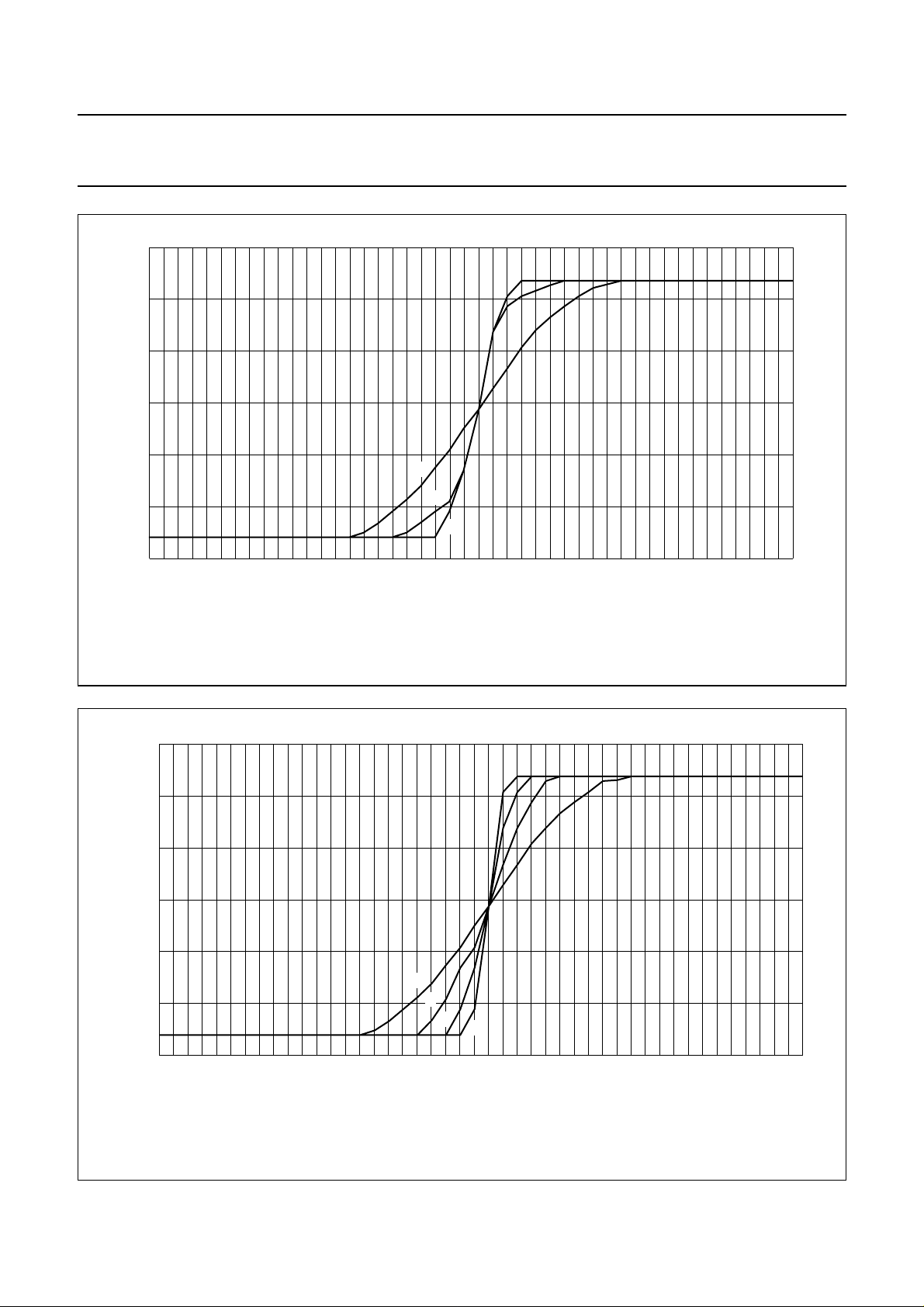
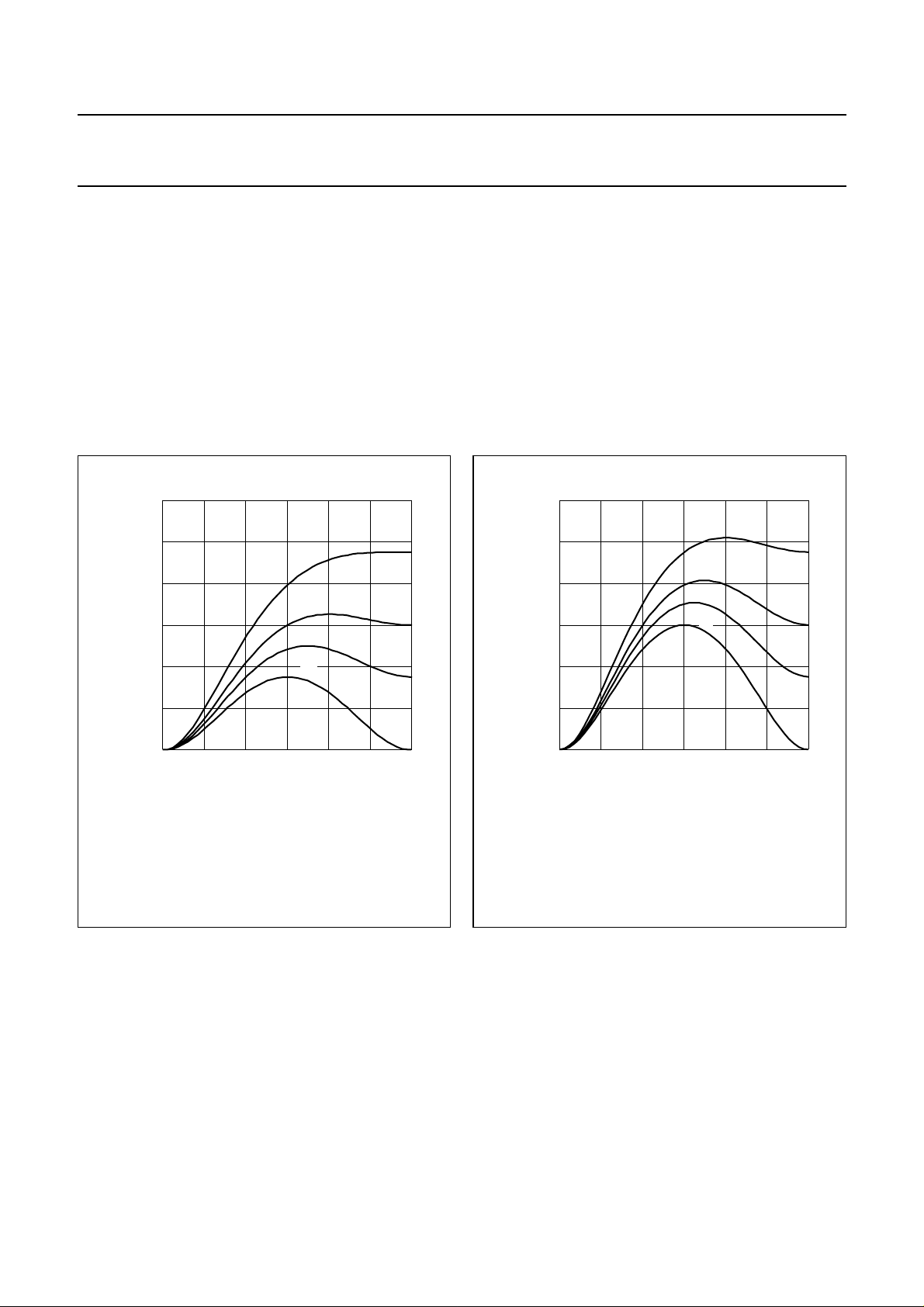
The DCTI function can be controlled by setting the range
to ±12, ±8, ±6 or ±4 pixels (see Fig.3) or by adjusting the
gain to 0,
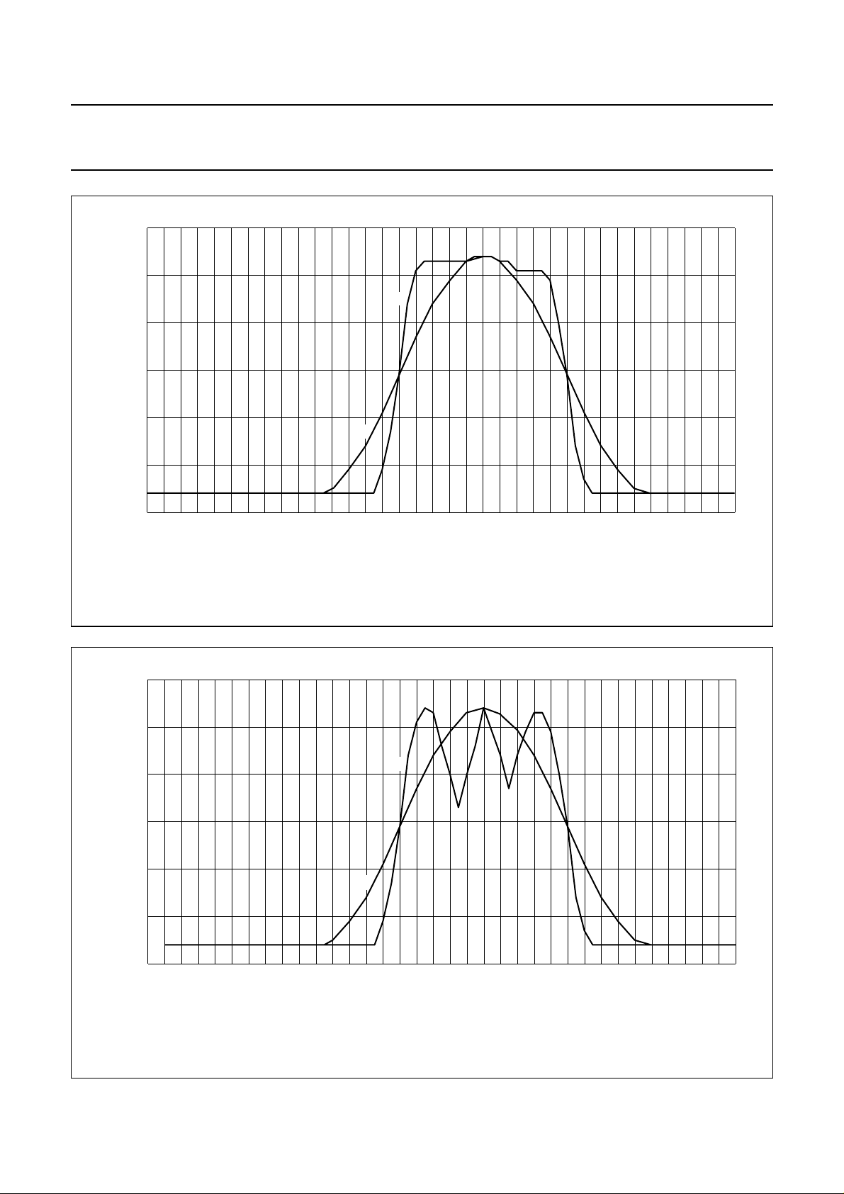
An artefact of this processing exists when two edges are
close together in the video. During the second half of the
first edge a delay is chosen that will collect video data
where the second edge is already active. The same is valid
for the second edge. The result of this processing on a
video pulse, which is looking like a hill, is that of a hill with
one or two bumps in it. To prevent this from happening, the
positions where the first derivatives in U and V change
sign, are marked and used to limit the range of the relative
delay. This function is called ‘over the hill protection’. It can
be turned on and off. Figures 5 and 6 show the effect of
the DCTI function with and without ‘over the hill protection’
when applied to a hill-shaped video pulse.
). The effect at an edge is that during the
1
⁄4,1⁄2 or 1.
Fig.2 Pin configuration.
1996 Oct 25 6
Philips Semiconductors Preliminary specification
Economical video processing IC
(ECOBENDIC)
120
handbook, full pagewidth
digital
signal
amplitude
100
80
60
110
(1) input signal.
(2) range = 4.
(3) range = 12.
(1)
SAA4970T
MGE093
(2)
(3)
20
40 45352515530
samples
Gain =1⁄2.
120
handbook, full pagewidth
digital
signal
amplitude
100
80
60
110
(1) input signal.
(2) gain = 0.25.
Fig.3 DCTI with variation of k range.
(1)
(2)
(3)
(4)
20
(3) gain = 0.5.
(4) gain = 1.
Range = 12.
MGE094
40 45352515530
samples
Fig.4 DCTI with variation of k gain.
1996 Oct 25 7
Philips Semiconductors Preliminary specification
Economical video processing IC
(ECOBENDIC)
120
handbook, full pagewidth
digital
signal
amplitude
100
(1) output.
(2) input.
80
60
20 30 90
(2)
(1)
5040
807060
Gain =1⁄2.
Range = ±12.
Hill protection = on.
SAA4970T
MGE095
samples
120
handbook, full pagewidth
digital
signal
amplitude
100
80
60
20 30 90
(1) output.
(2) input.
Fig.5 DCTI with ‘over the hill protection’.
(1)
(2)
5040
807060
Gain =1⁄2.
Range = ±12.
Hill protection = off.
MGE096
samples
Fig.6 DCTI without ‘over the hill protection’.
1996 Oct 25 8
Philips Semiconductors Preliminary specification
Economical video processing IC
(ECOBENDIC)
PEAKING
Peaking is implemented to obtain a higher gain in the
middle and upper ranges of the luminance bandwidth.
The filtering is an addition of:
• the original signal
• the original signal band-passed with centre
frequency =1⁄4f
• the original signal high-passed with maximum gain at
frequency =1⁄2fs.
12
handbook, halfpage
10
IH_PeakingI
(dB)
s
MGE097
(1)
8
(2)
6
(3)
SAA4970T
The band-passed and high-passed signals are weighted
with factors 0,
becomes [−α, −β, 1 + 2α +2β,−β, −α], where α is the
band-pass weighting factor and β the high-pass weighting
factor.
Coring is added to obtain no gain for low amplitudes in the
(high-pass + band-pass) signal, which is then considered
to be noise. Coring levels can be programmed as 0 (off),
+1/−2, +3/−4 and +7/−8 LSB at 10-bit word.
A limiter brings back the 11-bit range to a 9-bit range with
a clipping function on the lower and upper side.
handbook, halfpage
IH_PeakingI
(dB)
1
⁄8,1⁄4 and1⁄2. The impulse response
12
10
8
6
(1)
(2)
(3)
(4)
MGE098
(1) β =1⁄2.
(2) β =1⁄4.
(3) β =1⁄8.
(4) β =0.
4
2
0
0
1/4f
(4)
s
1/2f
Fig.7 Peaking transfer function with variation of β
(α =1⁄8).
4
2
0
s
(1) β =1⁄2.
(2) β =1⁄4.
(3) β =1⁄8.
(4) β =0.
0
1/4f
s
1/2f
s
Fig.8 Peaking transfer function with variation of β
(α =1⁄4).
1996 Oct 25 9
Philips Semiconductors Preliminary specification
Economical video processing IC
(ECOBENDIC)
MGE099
(1)
(2)
(3)
(4)
handbook, halfpage
IH_PeakingI
(dB)
(1) β =1⁄2.
(2) β =1⁄4.
(3) β =1⁄8.
(4) β =0.
16
14
12
10
8
6
4
2
0
0
1/4f
s
1/2f
SAA4970T
12
handbook, halfpage
10
IH_PeakingI
(dB)
8
6
4
2
0
s
(1) β =1⁄2.
(2) β =1⁄4.
(3) β =1⁄8.
0
1/4f
(1)
(2)
(3)
s
MGE100
1/2f
s
Fig.9 Peaking transfer function with variation of β
(α =1⁄2).
PHASE COMPENSATION
0.375
MGE101
f/f
Φ
nlp
(f/fs)
π
−1/2
− π
(1) λ =0.
(2) λ =1⁄8.
(3) λ =1⁄4.
(4) λ =1⁄2.
0
0 0.125 0.25 0.5
handbook, halfpage
(1)
(2)
(3)
(4)
Fig.11 Phase spectrum of NLP filter transfer
function.
Fig.10 Peaking transfer function with variation of β
(α = 0).
To compensate for a non-linear phase characteristic
before the A/D converter, this filter will compensate such
behaviour with a pulse response of [−λ, 1 + λ]. λ can be
programmed for the values 0,1⁄8,1⁄4 and1⁄2.
An 8-bit word width is re-obtained by means of clipping at
0 and 255.
F
RAMING AND BLANKING
Blanking is done with switching Y to value 16 and UV to
value 0 (in twos complement) on command of the BL
signal.
Framing is done by switching Y and the higher nibble of U
and V to certain programmable values (frame Y and
frame UV) on command of the signal KAD.
If the pixel repetition function is chosen the last values from
s
the video remain repeated instead of the fixed values.
The range of the output signal YO can be selected between
8 and 9 bits. In case of 8 bits for the nominal signal there
is room left for under and overshoot (adding up to a total of
9 bits); in case of selecting all 9 bits of the luminance D/A
converter for the nominal signal any under or overshoot
will be clipped.
1996 Oct 25 10
 Loading...