

Philips SAA2520GP Datasheet

INTEGRATED CIRCUITS
DATA SH EET
SAA2520
Stereo filter and codec for MPEG
layer 1 audio applications
Preliminary specification
File under Integrated Circuits, IC01
August 1993

Philips Semiconductors Preliminary specification
Stereo filter and codec for MPEG layer 1
audio applications
FEATURES
• Stereo filtering and codec functions in a single chip
• MPEG coded interface
• Filtered data interface
• Baseband audio data interface
• LT interface to microcontroller
• Clock generator
• Low operating voltage capability.
ORDERING INFORMATION
EXTENDED TYPE
NUMBER
SAA2520GP
(1)
Note
1. SOT205-1; 1996 August 26.
PINS PIN POSITION MATERIAL CODE
44 QFP plastic SOT205AG
SAA2520
GENERAL DESCRIPTION
The SAA2520 performs the sub-band filtering and audio
frame codec functions to provide efficient audio
compression/decompression for MPEG (11172-3) Layer1
applications. It is capable of functioning as a stand-alone
decoder but requires the addition of an adaptive masking
threshold processor (SAA2521) in order to function as a
highly efficient encoder.
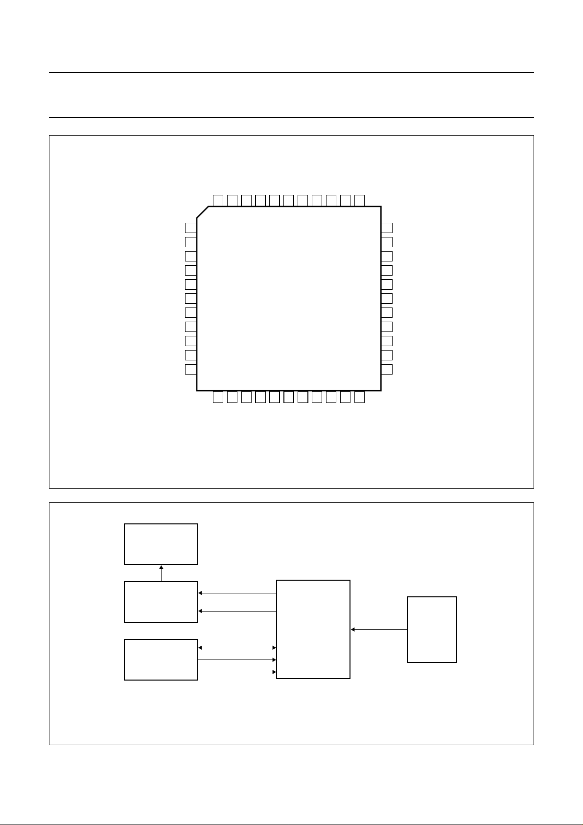
PACKAGE
handbook, full pagewidth
FS256
SBDIR
SBEF
SWS
SCL
SDA
1
7
11
20
19
21
CLK24 X22OUT X24OUT
CLK22 X22IN X24IN
38 39 40 41 42 43 28,44
CLOCK GENERATOR
STEREO
SUB-BAND
FILTER
PROCESSOR
BASEBAND
INTERFACE
5,37
V
SS
SERIAL
FILTERED
DATA
INTERFACE
FDAF
FDAC FSYNC
V
DD
15
FRESET
SAA2520
CODEC
14 13 36 35 34 33 32 22 29 618 17 16
SYNCDAI
FDIR
SUB-BAND
SERIAL
INTERFACE
MICROPROCESSOR
INTERFACE & CONTROL
LTCLK
LTCNT1 LTENA
PWRDWN
LTDATA
RESET
8
SBDA
9
SBCL
10
SBWS
12
SBMCLK
2
MUTEDAC
3
DEEMDAC
4
ATTDAC
MLB125
URDALTCNT0
Fig.1 Block diagram.
August 1993 2
Philips Semiconductors Preliminary specification
Stereo filter and codec for MPEG layer 1
audio applications
DD
X24IN
42
X22IN
X22OUT
41
40
SAA2520
handbook, full pagewidth
FS256
MUTEDAC
DEEMDAC
ATTDAC
V
SS
URDA
SBDIR
SBDA
SBCL
SBWS
SBEF
V
X24OUT
44
43
1
2
3
4
5
6
7
8
9
10
11
CLK24
39
V
CLK22
38
SS
LTCNT1
373635
LTCNT0
LTENAPWRDWN
34
33
32
31
30
29
28
27
26
25
24
23
LTCLK
LTDATA
T0
T1
RESET
V
DD
DSC0
DSC1
DSC2
DSC3
DSC4
SAA2520
handbook, full pagewidth
AUDIO
AMPLIFIER
DAC
MICROCONTROLLER
12
13
14
15
FDIR
SYNCDAI
FRESET
SBMCLK
Fig.2 Pin configuration.
digital audio interface
control
system micro interface
power down
reset
16
17
FDAF
FSYNC
18
19
SCL
FDAC
SAA2520
20
SWS
21
SDA
22
MLB126
MPEG interface
MPEG
source
MLB127
Fig.3 MPEG decoder system data flow diagram.
August 1993 3

Philips Semiconductors Preliminary specification
Stereo filter and codec for MPEG layer 1
SAA2520
audio applications
PINNING
SYMBOL PIN DESCRIPTION TYPE
2
FS256 1 (Filtered)-I
input with pull-down
MUTEDAC 2 DAC control/output expander O
DEEMDAC 3 DAC control/output expander O
ATTDAC 4 DAC control/output expander O
V
SS
5 supply ground (0 V)
URDA 6 unreliable drive processing data; CMOS level I
SBDIR 7 sub-band I
SBDA 8 sub-band I
SBCL 9 sub-band I
SBWS 10 sub-band I
SBEF 11 sub-band I
SBMCLK 12 sub-band I
input with pull-down
SYNCDAI 13 DAI synchronization pulse O
FDIR 14 (Filtered)-I
FRESET 15 reset signal for SAA2521 O
FSYNC 16 Filtered-I
FDAF 17 Filtered-I
pull-down
FDAC 18 Filtered-I
pull-down
SCL 19 I
SWS 20 I
SDA 21 I
2
S bit clock; 4 mA, 3-state output + CMOS input with pull-down I/O
2
S-word select; 4 mA, 3-state output + CMOS input with pull-down I/O
2
S baseband data filter; 4 mA, 3-state output + CMOS input with pull-down I/O
PWRDWN 22 power-down mode; CMOS level I
DSC4 23 test pin
DSC3 24 test pin
DSC2 25 test pin
DSC1 26 test pin
DSC0 27 test pin
V
DD
28 positive supply voltage (+5 V)
RESET 29 system reset; CMOS level with pull-down and hysteresis I
T1 30 test pin; do not connect
T0 31 test pin; do not connect
LTDATA 32 LT interface data; 4 mA, 3-state output + CMOS input with pull-down I/O
LTCLK 33 LT interface bit clock; CMOS level I
S clock; 256 × sample frequency. 12 mA 3-state output + CMOS
2
S direction: (SWBS, SBCL, SBDA); CMOS level I
2
S data; 4 mA, 3-state output + CMOS input with pull-down I/O
2
S bit clock; 4 mA, 3-state output + CMOS input with pull-down I/O
2
S word select; 4 mA, 3-state output + CMOS input with pull-down I/O
2
S byte error flag; CMOS level I
2
S clock, 6.144 MHz locked to FS256; 8 mA, 3-state output + CMOS
2
S direction: (FDAC, FDAF, SDA); O
2
S sync signal for SAA2521 O
2
S sub-band filter data; 4 mA, 3-state output + CMOS input with
2
S sub-band codec data; 4 mA, 3-state output + CMOS input with
I/O
O
I/O
I/O
August 1993 4
Philips Semiconductors Preliminary specification
Stereo filter and codec for MPEG layer 1
SAA2520
audio applications
SYMBOL PIN DESCRIPTION TYPE
LTENA 34 LT interface enable; CMOS level I
LTCNT0 35 LT interface control; CMOS level I
LTCNT1 36 LT interface control; CMOS level I
V
SS
CLK22 38 22.5792 MHz buffered output O
CLK24 39 24.576 MHz buffered output O
X22IN 40 22.5792 MHz crystal input I
X22OUT 41 22.5792 MHz crystal output O
X24IN 42 24.576 MHZ crystal input I
X24OUT 43 24.576 MHz crystal output O
V
DD
37 supply ground (0 V)
44 positive supply voltage (+5 V)
August 1993 5

Philips Semiconductors Preliminary specification
Stereo filter and codec for MPEG layer 1
audio applications
handbook, full pagewidth
ALLOCATION &
SCALE FACTOR
INFORMATION
TABLE
SCALING &
QUANTIZATION
Fig.4 Encoding mode.
base band
samples
from SAA2521
SUB-BAND
FILTER
sub - band
samples
allocation information
and scale factor indices
SYNC AND
CODING
INFORMATION
quantized samples
FORMATTER
MLB128
SAA2520
MPEG
OUTPUT
DATA
handbook, full pagewidth
MPEG
input
data
FORMATTER
DE–
sync/coding
allocation
scale factor
quantized
samples
CONTROL
SCALE
FACTOR
ARRAY
& ALLOCATION
DEQUANTIZATION
Fig.5 Decoding mode.
MULTIPLY
OUTPUT
CONTROL
sub-band
samples
MLB129
SUB-BAND
FILTER
base band
samples
August 1993 6

Philips Semiconductors Preliminary specification
Stereo filter and codec for MPEG layer 1
audio applications
FUNCTIONAL DESCRIPTION
Coding System
MPEG coding achieves highly efficient digital encoding of
audio signals by using an algorithm based on the
characteristics of the human auditory system.
The broad-band audio signal is split into 32 sub-band
signals during encoding. For each of the sub-band signals
the masking threshold is calculated. The samples of the
sub-bands are incorporated in the signal with an accuracy
that is determined by the signal to masking threshold ratio
for that sub-band.
During decoding, the sub-band signals are reconstructed
and combined into a broadband audio signal. The
integrated filter processor performs the splitting (encoding)
and joining (decoding) including the corresponding
formatting functions.
For encoding, a SAA2521 is necessary to calculate the
masking threshold and required accuracy of the sub-band
samples.
SAA2520
After sync and coding information, allocation data and the
scale factors are used to correctly fill the scale factor array.
This is followed by a process of multiplication to provide
de-quantization and de-scaling of the samples.
The decoded sub-band samples, which are represented in
24-bit two's complement notation, are processed by the
sub-band filters and reconstituted into a single digital audio
signal.
RESET
Reset must be active under the following conditions:
1. From system power-up until CLK24 has executed
more than 24 clock cycles.
2. From the falling edge of PWRDWN for a period
equivalent to 24 cycles of CLK24 + oscillator start-up
time. This is typically >1 ms, however, this value is
crystal dependent.
PWRDWN
Encoding (See Fig.4)
An encoding algorithm table is used during the coding
process but, due to the Adaptive Allocation functions of the
SAA2521, this may change with every frame. The table is
therefore calculated for each frame by the SAA2521 and
then transferred to the SAA2520.
A frame contains 2 × 384 samples of Left and Right audio
data. This results in 12 samples per sub-band
(32 sub-bands). The samples of the greatest amplitude are
used to determine the scale factor for a given sub-band.
All samples are then scaled to represent a fraction of the
greatest amplitude.
Once scaled, the samples are quantized to reduce the
number of bits to correspond with the allocation table as
calculated by the SAA2521. Synchronization and coding
information data is then added to result in a fully encoded
MPEG signal.
Decoding (See Fig.5)
All essential information (synchronization, system
information, scale factors and encoded sub-band
samples) are conveyed by incoming data. Decoding is
repeated for every frame.
A HIGH input applied to this pin will halt all internally
generated clock signals. As a result, chip activity will halt
completely with outputs frozen in the state which was
current at the time of PWRDWN activation.
The bi-directional outputs: LTDATA, FDAC, FDAF, SDA,
SBWS, SBCL and SBDA will be 3-stated.
Crystal Oscillators
A 24.576 MHz crystal together with some external
components form the 24.576 MHz oscillator (pins 42 and
43). Similarly a 22.5792 MHz oscillator (pins 40 and 41) is
formed by similar peripheral components together with an
appropriate crystal (see Fig.6).
The component values shown apply only to crystals from
the Philips 4322 156 series which exhibit an equivalent
series resistance of ≤ 40 Ω.
August 1993 7
Philips Semiconductors Preliminary specification
Stereo filter and codec for MPEG layer 1
audio applications
handbook, full pagewidth
Component values apply only to crystals from the Philips 4322 156 series.
C2 33 pF
C1 33 pF
C3 33 pF
C4 33 pF
22.5792
MHz
X1
24.576
MHz
X2
R1
1 MΩ
R2 1 kΩ
R4
1 MΩ
R3 1 kΩ
X22OUT
X24OUT
Fig.6 Crystal oscillator components.
X22IN
X24IN
SAA2520
40
41
42
43
SAA2520
MLB130
channel
SWS
SCL
SDA
bit :
left 32 bits
1
MSB LSB
18 bits
4
0001716151
210
13 bits
Fig.7 Transfer of SDA data (Standard I2S default format).
1716151
MSB
right
4
MLA923 - 2
August 1993 8

Philips Semiconductors Preliminary specification
Stereo filter and codec for MPEG layer 1
audio applications
channel
SWS
SCL
SDA
bit :
18 bits
1
3
4
MSB LSB
Fig.8 Transfer of SDA data (alternative format).
left 32 bits
0001716151
210
14 bits
1716151
MSB
SAA2520
right
4
MLA924 - 2
channel
SWS
SCL
FDAC/
FDAF
bit :
left 32 bits
1
2322212
MSB LSB
02010
0
Fig.9 Transfer of FDAF and FDAC (filtered) data.
right
7 bits
0
2322212
MSB
0
MLA925 - 2
August 1993 9
Philips Semiconductors Preliminary specification
Stereo filter and codec for MPEG layer 1
audio applications
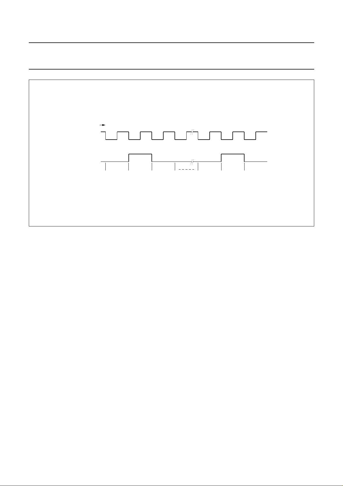
channel
SWS
FSYNC
sub-band
LRLLLLLLRRRRRR
31 0 1 31 0 1
Fig.10 SWS related to phase of FSYNC.
SAA2520
MBC148 - 1
Baseband Interface Signals
The interface between the SAA2520 and the baseband input/output circuitry consists of the following signals:
SWS bi-directional word (channel) select FS
SCL bi-directional bit clock 64FS
SDA bi-directional baseband data
FDIR output decoding mode (direction control)
The SWS signal indicates the channel of the sample signal
(either LEFT or RIGHT) and is equal to the sampling
frequency FS.
Operating at a frequency of 64 times that is used for
sampling, the bit clock dictates that each SWS period
contains 64 SDA data bits. Of these, a maximum of 36 are
used to transfer data (samples may have a length up to
18-bits). Samples are transferred most significant bit first.
Both SWS and SDA change state at the negative edge of
SCL.
This baseband data is transferred between the SAA2520
and the input/output using either Standard I2S (default) or
the alternative format shown in Fig.8.
August 1993 10

Philips Semiconductors Preliminary specification
Stereo filter and codec for MPEG layer 1
audio applications
Interface between SAA2520 and SAA2521 consists of the following signals:
ILTERED-I
F
SWS bi-directional word select (common to I2S) FS
SCL bi-directional bit clock (common to I
FDAC bi-directional codec data
FDAF bi-directional filter data
FSYNC output synchronization FS/32
Filtered data is transferred between SAA2520 filter/codec
functions and the SAA2521 using the format shown in
Fig.9.
The frequency of the SWS signal is equal to the sample
frequency FS and the bit clock SCL is 64 times the sample
frequency. Each period of SWS contains 64 data-bits, 48
of which are used to transfer data. The half period in which
SWS is LOW is used to transfer the information of the
LEFT channel while the following half period during which
SWS is HIGH carries the data of the RIGHT channel.
The 24-bit samples are transferred most significant bit first.
This bit is transferred in the bit clock period with a 1-bit
delay following the change in SWS. Both SWS and
FDAF/FDAC change state at the negative edge of SCL.
The SAA2521 may be synchronized to the sub-band
codec using the FSYNC signal, which defines the SWS
period in which the samples of sub-band 0 (containing the
lowest frequency components) are transferred
(see Fig.10).
SAA2521
The operation of SAA2521 and the input/output circuitry is
controlled by three signals shown in Table 1.
2
S INTERFACE
AND INPUT/OUTPUT MODE CONTROL
2
S) 64FS
MPEG C
The interface that carries the MPEG coded signal uses
the following signals:
The MPEG I
SBWS bi-directional word selection
SBCL bi-directional bit clock
SBDA bi-directional sub-band coded data
SBEF input error signal
Operation is further controlled by:
SBDIR input direction of data flow
URDA input unreliable encoded data signal
The SBMCLK signal is the main frequency from which
other clock signals are derived. In encode mode this
division is performed internally. In decode mode the
external source should provide SBWS and SBCL.
The frequency of the signal is equal to 1/32nd of the bit
rate. The frequency of the bit clock SBCL is twice that of
the bit rate. Some examples of the frequencies are given
in Table 2.
ODED INTERFACE
2
S interface
SAA2520
FRESET and SYNCDAI are given whenever:
− FS256, SCL and SWS outputs switch between
high and low impedance
− FS256 frequency is changed
(12.288/11.2896/8.192 MHz)
− FDIR is switching
− bit rate is changing
− system reset is active
August 1993 11
 Loading...