

Philips saa2502 DATASHEETS

INTEGRATED CIRCUITS
DATA SH EET
SAA2502
ISO/MPEG Audio Source Decoder
Preliminary specification
Supersedes data of 1997 Apr 18
File under Integrated Circuits, IC01
1997 Nov 17

Philips Semiconductors Preliminary specification
ISO/MPEG Audio Source Decoder SAA2502
CONTENTS
1 FEATURES
2 APPLICATIONS
3 GENERAL DESCRIPTION
4 ORDERING INFORMATION
5 BLOCK DIAGRAM
6 PINNING
7 FUNCTIONAL DESCRIPTION
7.1 Basic functionality
7.2 Clock generator module
7.2.1 External sample clock
7.2.2 Free running internal sample clock
7.2.3 Locked internal sample clock
7.2.4 Limited sampling frequency support for internal
sampling clocks
7.3 Input interface module
7.3.1 Master input mode
7.3.2 Slave input mode
7.3.3 Buffer controlled input mode
7.4 Decoder core
7.4.1 Frame synchronization to input data streams
7.4.2 Master input mode bit rate generation
7.4.3 Sample clock generation
7.4.4 Decoder precision
7.4.5 Scale factor CRC protection
7.4.6 Handling of errors in the coded input data
7.4.7 Dynamic range compression
7.4.8 Baseband audio processing
7.4.9 Decoder latency time
7.5 Output interface module
7.5.1 I2S output
7.5.2 SPIDF output
7.5.3 Bit serial analog output
7.6 Control interface module
7.6.1 Resetting
7.6.2 Interrupts
7.6.3 Microcontroller interface
7.6.4 Initialization
7.6.5 Transfer protocols
7.6.6 Local registers
8 APPENDIX
8.1 L3 interface specification
8.1.1 Introduction
8.1.2 Example of a data transfer
8.1.3 Timing requirements
8.1.4 Timing
9 LIMITING VALUES
10 DC CHARACTERISTICS
11 AC CHARACTERISTICS
11.1 Host interface: CDATA, CCLK and CMODE
12 APPLICATION INFORMATION
13 PACKAGE OUTLINE
14 SOLDERING
14.1 Introduction
14.2 Reflow soldering
14.3 Wave soldering
14.4 Repairing soldered joints
15 DEFINITIONS
16 LIFE SUPPORT APPLICATIONS
1997 Nov 17 2

Philips Semiconductors Preliminary specification
ISO/MPEG Audio Source Decoder SAA2502
1 FEATURES
• Low sampling frequency decoding possibilities (24 kHz,
22.05 kHz and 16 kHz) of MPEG2 are supported
• A variety of output formats are supported: I2S, SPDIF
and 256 or more times oversampled bit serial analog
stereo
• Automatic internal dynamic range compression
algorithm using programmable compression
parameters
• Non byte-aligned coded input data is handled
• Built-in provisions to generate high quality sampling
clocks for all six supported sampling frequencies; these
sampling clocks may locked to an external PLL to
support an extensive list of input data reference clock
frequencies
• Bit-rate and sampling-rate settings may be overruled by
the microcontroller while the SAA2502 is trying to
establish frame synchronization
• Input interface mode which requests data based on
input buffer content, enables the handling of variable
bit-rate input streams and input data offered in (fixed
length) bursts
• An interrupt output pin which can generate interrupt
requests at the occurrence of various events;
consequently polling by the microcontroller is not
needed in most situations
2
• L3 and the I
are supported
• The control interface is always fully operational (also
while STOP is asserted)
• CRC protection of scale factors is provided for all
supported sample frequencies.
C-bus microcontroller interface protocols
2 APPLICATIONS
• Astra Digital Radio (ADR)
• Digital Audio Broadcast (DAB)
• Digital Versatile Disc (DVD)
• Digital Video Broadcast (DVB)
• General purpose MPEG2 audio decoding.
3 GENERAL DESCRIPTION
The SAA2502 is a second generation ISO/MPEG audio
source decoder. The device specification has been
enhanced with respect to the SAA2500 and SAA2501 ICs
and therefore it offers in principle all features of its
predecessors.
It supports layer I and II of MPEG1 and the MPEG2
requirements for a stereo decoder.
4 ORDERING INFORMATION
PACKAGE
TYPE NUMBER
NAME DESCRIPTION VERSION
SAA2502H QFP44 plastic quad flat package; 44 leads (lead length 1.3 mm);
body 10 × 10 × 1.75 mm
1997 Nov 17 3
SOT307-2
Philips Semiconductors Preliminary specification
ISO/MPEG Audio Source Decoder SAA2502
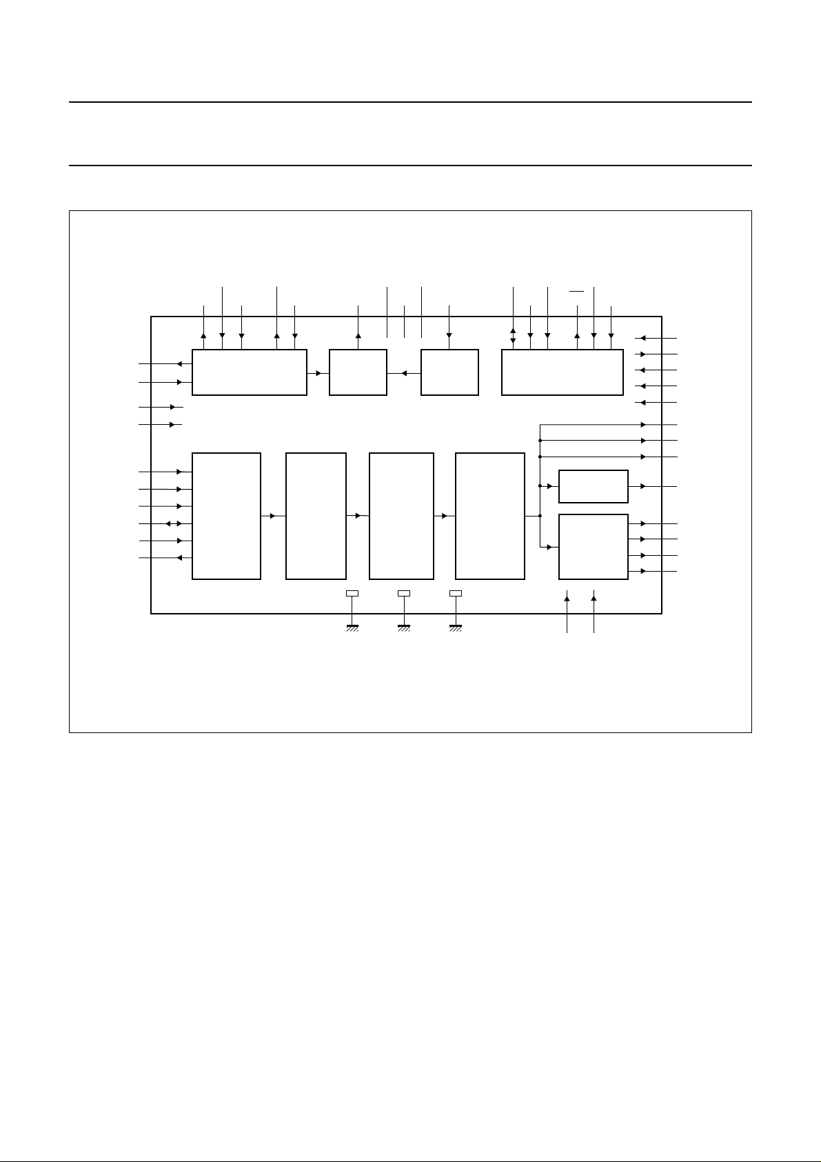
5 BLOCK DIAGRAM
handbook, full pagewidth
FSCLK
FSCLKIN
TC0
TC1
CD
CDEF
CDSY
CDCL
CDVAL
CDRQ
MCLKOUT
1
25
40
43
15
17
19
14
20
13
MCLKIN
31
CLOCK GENERATOR
INPUT
INTERFACE
MCLK24
X22OUT
X22IN
DEMULTI-
PLEXER
CMODE
CCLK
7
8222326272932
DECODING
CONTROL
PHDIF
PHASE
COMPA-
RATOR
VDD1
VDD2
18 30 44
VDD3
CDATA
REFCLK
DIVIDER
SAA2502
DEQUANTI-
ZATION
AND
SCALING
16 28 42 37 36
GND1
GND2
SYNTHESIS
SUB-BAND
GND3
FILTER
REFP
STOP
INT
RESET
SPDIF
ENCODER
DIGITAL-TO-
ANALOG
CONVERTER
REFN
1112109
33
41
24
21
39
38
34
35
MGE469
5
3
2
4
6
TDI
TDO
TCK
TMS
TRST
SD
SCK
WS
SPDIF
LFTPOS
LFTNEG
RGTPOS
RGTNEG
Fig.1 Block diagram.
1997 Nov 17 4
Philips Semiconductors Preliminary specification
ISO/MPEG Audio Source Decoder SAA2502
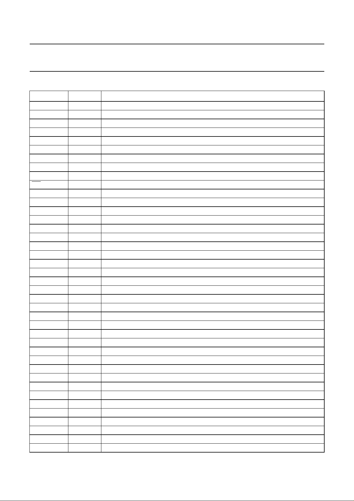
6 PINNING
SYMBOL PIN DESCRIPTION
FSCLK 1 sample rate clock output; buffered signal
SCK 2 baseband audio data I2S clock output
SD 3 baseband audio I
WS 4 baseband audio data I
TRST 5 boundary scan test reset input
SPDIF 6 SPDIF baseband audio output
CCLK 7 L3 clock/I
CDATA 8 L3 data/I
2
2
C-bus serial data input/output; note 1
CMODE 9 L3 mode (address/data select input)
INT 10 interrupt request output; active LOW; note 1
RESET 11 master reset input
STOP 12 soft reset/stop decoding input
CDRQ 13 coded data request output
CDCL 14 coded data bit clock input/output; note 2
CD 15 MPEG coded data input
GND1 16 ground 1
CDEF 17 coded data error flag input
V
DD1
18 supply voltage 1
CDSY 19 coded data byte or frame sync input
CDVAL 20 coded data valid flag input
TMS 21 boundary scan test mode select input
REFCLK 22 PLL reference clock input
PHDIF 23 PLL phase comparator output; note 2
TCK 24 boundary scan test clock input
FSCLKIN 25 sample rate clock input
X22IN 26 22.579 MHz clock oscillator input or signal input
X22OUT 27 22.579 MHz clock oscillator output
GND2 28 ground 2
MCLK24 29 master clock frequency indication input
V
DD2
30 supply voltage 2
MCLKOUT 31 master clock oscillator output
MCLKIN 32 master clock oscillator input or signal input
TDI 33 boundary scan test data input
RGTPOS 34 analog right channel positive output
RGTNEG 35 analog right channel negative output
REFN 36 low reference voltage input for analog outputs
REFP 37 high reference voltage input for analog outputs
LFTNEG 38 analog left channel negative output
LFTPOS 39 analog left channel positive output
TC0 40 factory test scan chain control 0 input
2
S data output
2
S word select output
C-bus bit clock input
1997 Nov 17 5
Philips Semiconductors Preliminary specification
ISO/MPEG Audio Source Decoder SAA2502
SYMBOL PIN DESCRIPTION
TDO 41 boundary scan test data output
GND3 42 ground 3
TC1 43 factory test scan chain control 1 input
V
DD3
Notes
1. Output type is: open-drain.
2. Output type is: 3-state.
44 supply voltage 3
DD3
V
44
TC1
43
GND3
42
TDO
41
TC0
40
LFTNEG
LFTPOS
39
38
REFP
37
REFN
36
RGTPOS
RGTNEG
35
34
FSCLK
SCK
SD
WS
TRST
SPDIF
CCLK
CDATA
CMODE
INT
RESET
22
REFCLK
33
32
31
30
29
28
27
26
25
24
23
MGE468
TDI
MCLKIN
MCLKOUT
V
DD2
MCLK24
GND2
X22OUT
X22IN
FSCLKIN
TCK
PHDIF
1
2
3
4
5
6
7
8
9
10
11
12
13
STOP
CDRQ
14
CDCL
SAA2502
15
16
CD
GND1
17
CDEF
18
DD1
V
19
CDSY
21
20
TMS
CDVAL
Fig.2 Pin configuration.
1997 Nov 17 6
Philips Semiconductors Preliminary specification
ISO/MPEG Audio Source Decoder SAA2502
7 FUNCTIONAL DESCRIPTION
7.1 Basic functionality
From a functional point of view, several blocks can be
distinguished in the SAA2502. A clock generator section
derives the internally and externally required clock signals
from its clock inputs. The input interface section receives
or requests coded input data in one of the supported input
interface modes. The demultiplexer processor handles
frame synchronization, parsing, demultiplexing and error
concealment of the input data stream The de-quantization
and scaling processor performs the transformation and
scaling operations on the (demultiplexed) coded sample
representations in the input bitstream to yield sub-band
domain samples.
The sub-band samples are transferred to the synthesis
sub-band filter bank processor which reconstructs the
baseband audio samples. The output interface block
transforms the audio samples to the output formats
required by the different output ports.
The decoding control block houses the I
microcontroller interface, and handles the response to
external control signals. This section enables the
application to configure the SAA2502, to read its decoding
status, to read ancillary data and so on.
2
C-bus/L3
7.2 Clock generator module
The SAA2502 clock interfacing is designed for application
versatility. It consists of 9 signals (see Table 1).
The clock generator provides the following clock signals:
• Internal sample clocks
• External buffered sample clock FSCLK
• Processor master clock
• Coded input data bit clock
• Coded input data request clock
The module can be configured to operate in 3 different
modes of operation:
• External sample clock mode
• Free running internal sample clock mode
• Locked internal sample clock mode.
Clock generator operation mode must be stationary while
the device is in normal operation. Changing mode should
always be followed by a (soft) reset.
input bitrate
f
=
----------------------------------32
Several pins are reserved for boundary scan test (5 pins)
and factory test scan chain control (2 pins).
Table 1 Clock interfacing signals
SIGNAL DIRECTION FUNCTION
MCLKIN input master clock oscillator input or signal input
MCLKOUT output master clock oscillator output
MCLK24 input master clock frequency indication
X22IN input 22.5792 MHz clock oscillator input or signal input
X22OUT output 22.5792 MHz clock oscillator output
FSCLKIN input external sample rate clock signal input
FSCLK output sample rate clock signal output
REFCLK input coded input data rate reference clock
PHDIF output phase difference indication output between reference clock and sample clock
1997 Nov 17 7
Philips Semiconductors Preliminary specification
ISO/MPEG Audio Source Decoder SAA2502
7.2.1 EXTERNAL SAMPLE CLOCK
In applications where a 256 × fs sample clock is available,
the use of external crystals may be avoided by putting the
SAA2502 clock generator module in ‘external sample
clock mode’. Such mode setting may be realized by setting
control flag FSCINP of the control interface. In this event
the sample clock has to be provided to the FSCLKIN clock
input. If sample rate switching should be supported,
required clock frequency changes are the responsibility of
the application. After such a clock frequency change,
enforcement of a soft reset is advised.
In external sample clock mode (and only in that mode) the
clock generator module is able to accept a 384 × f
sample
s
clock input. If that mode of operation is desired the control
flag FSC384 should be set.
The FSCLK output is normally disabled in this mode.
If enabled (by setting control flag FSCENA) FSCLK will
produce a buffered copy of FSCLKIN.
X22IN, X22OUT, REFCLK and PHDIF are not used in this
mode. X22IN and REFCLK should be connected to GND
or VDD.
MCLKIN is used to provide the (free running) master clock.
This may either be achieved by applying a correct clock
signal to MCLKIN or by connecting a crystal between
MCLKIN and MCLKOUT. In external sample clock mode
(and only in that mode) the master clock may deviate from
24.576 MHz. The master clock frequency value required
depends on the state of pin MCLK24 (see Table 2).
Table 2 Master clock frequency setting by MCLK24
FREQUENCY
MCLK24
MINIMUM MAXIMUM
GND 256 × f
s
12.288 MHz
(256 × 48 kHz)
V
DD
512 × f
s
24.576 MHz
(512 × 48 kHz)
7.2.2 FREE RUNNING INTERNAL SAMPLE CLOCK
This is the default mode of operation: 256 × fs for all six
supported sample rates is generated internally from the
clock frequencies supplied to MCLKIN (24.576 MHz) and
X22IN (22.5792 MHz) as shown in Table 3.
Table 3 Internal sample clock (default mode)
SAMPLE
FREQUENCY
256 × 48 kHz 12.288
256 × 44.1 kHz 11.2896
256 × 32 kHz 8.192
256 × 24 kHz 6.144
256 × 22.05 kHz 5.6448
256 × 16 kHz 4.096
RESULTANT FREQUENCIES
(MHz)
24.576
----------------- 2
22.5792
--------------------2
24.576
----------------- 3
24.576
----------------- 4
22.5792
--------------------4
24.576
----------------- 6
(1)
Note
1. Asymmetrical FSCLK.
The main advantage of this mode is that the SAA2502
determines automatically which sampling rate is active
from the sampling rate setting of the input data bit stream,
and then selects either MCLKIN or X22IN divided by the
correct number as the sample clock source.
Therefore this mode is particularly suited in applications
supporting dynamically varying sampling rates.
The required clocks may either be applied to MCLKIN
(respectively to X22IN) or be generated by connecting a
crystal between MCLKIN and MCLKOUT (respectively
between X22IN and X22OUT).
The recommended crystal oscillator configuration is
shown in Fig.3. The specified component values only
apply to crystals with a low equivalent series resistance
of <40 Ω.
FSCLKIN, REFCLK and PHDIF are not used in this mode
(FSCLKIN and REFCLK should be connected to V
SS
or
VDD). MCLK24 has to be connected to VDD, while the
control flags FSCINP and FSC384 should be left in their
default (cleared) states. If the FSCLK output is enabled (by
setting control flag FSCENA) FSCLK will produce a
buffered version of 256 × fs.
1997 Nov 17 8
Philips Semiconductors Preliminary specification
ISO/MPEG Audio Source Decoder SAA2502
in such a way that SIG and 256 × fs will stem from the
handbook, halfpage
C1 = C2 = C3 = C4 = 10 pF;
R1 = R4 = 100 kΩ;
R2=R3=1kΩ;
X1 = 22.5792 MHz;
X2 = 24.5760 MHz.
C2
C1
C3
C4
X1
X2
26
R1
R2
27
32
R4
R3
31
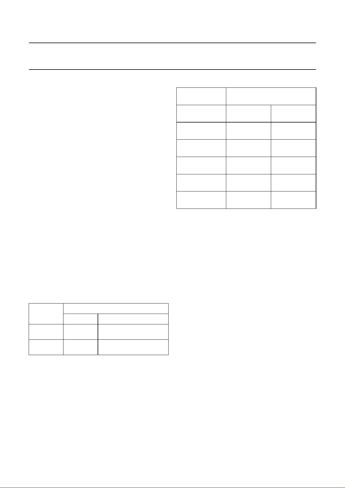
Fig.3 Crystal oscillator components.
7.2.3 LOCKED INTERNAL SAMPLE CLOCK
SAA2502
MGE470
same source. The divisor N1 is programmable with
(1 to 16) × 8 as possible values.
REF on the other hand is derived from the REFCLK input.
Two programmable dividers in series are used here. N
2
may adopt one of 4 possible values: 5, 25, 125 or 625
while N3 can be programmed to be 1 to 32. Because both
inputs of the phase comparator have to operate at identical
frequencies the next equation has to be obeyed:
REFCLK
------------------------- -
×
N
2N3
REFCLK
156.6 kHz
=
--------------------------N
153.6 kHz N
=
----------------------------------------------------- -
or, written differently:
1
× N3×
N
1
2
For a list of supported REFCLK frequency values
see Chapter 8.
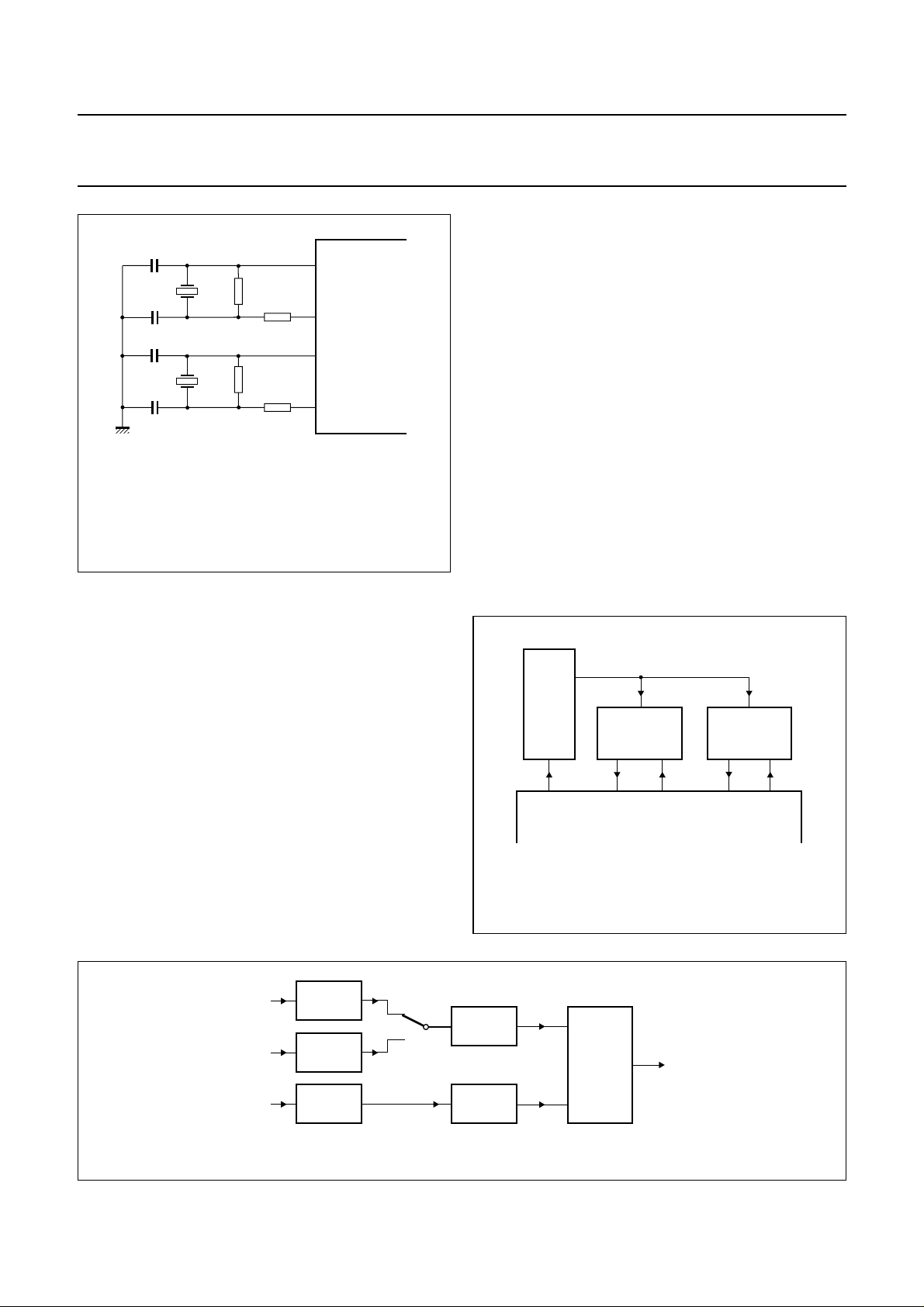
The mode of operation of the phase comparator in Fig.5 is
programmable via the control flag PHSMOD:
This mode differs from the previous one in just a single
aspect: the REFCLK and PHDIF pins are used to realize a
Phase-Locked Loop (PLL) which locks the 256 × fs sample
clock to the REFCLK reference clock. Because the real
goal is locking sample clock and bit rate, a reference clock
should be used which has a fixed relation to the input bit
rate. An example of such a PLL realization is shown in
Fig.4.
The phase comparator output PHDIF generates a signal
with a DC component proportional to the phase difference
between the internal signals SIG and REF (see Fig.5).
The 22.5792 MHz signal X22IN is divided by 147 and the
24.576 MHz signal MCLKIN is divided by 160. This results
in the same frequency (153.6 kHz) in both events.
One of the two signals is selected as input for the
programmable divide by N
handbook, full pagewidth
unit. The selector is controlled
1
X22IN
MCLKIN
REFCLK
DIVIDE BY
147
DIVIDE BY
160
DIVIDE BY
N
2
153.6 kHz
Fig.5 SAA2502 phase comparator.
handbook, halfpage
DIVIDE BY
N
1
DIVIDE BY
N
3
LOWPASS
FILTER
PHDIF MCLKIN MCLKOUT X22IN X22OUT
24.576 MHz
VCXO
22.5792 MHZ
VCXO
SAA2502
MGE471
Fig.4 External PLL components.
SIG
PHASE
COMPA-
RATOR
REF
MGE472
PHDIF
1997 Nov 17 9
Philips Semiconductors Preliminary specification
ISO/MPEG Audio Source Decoder SAA2502
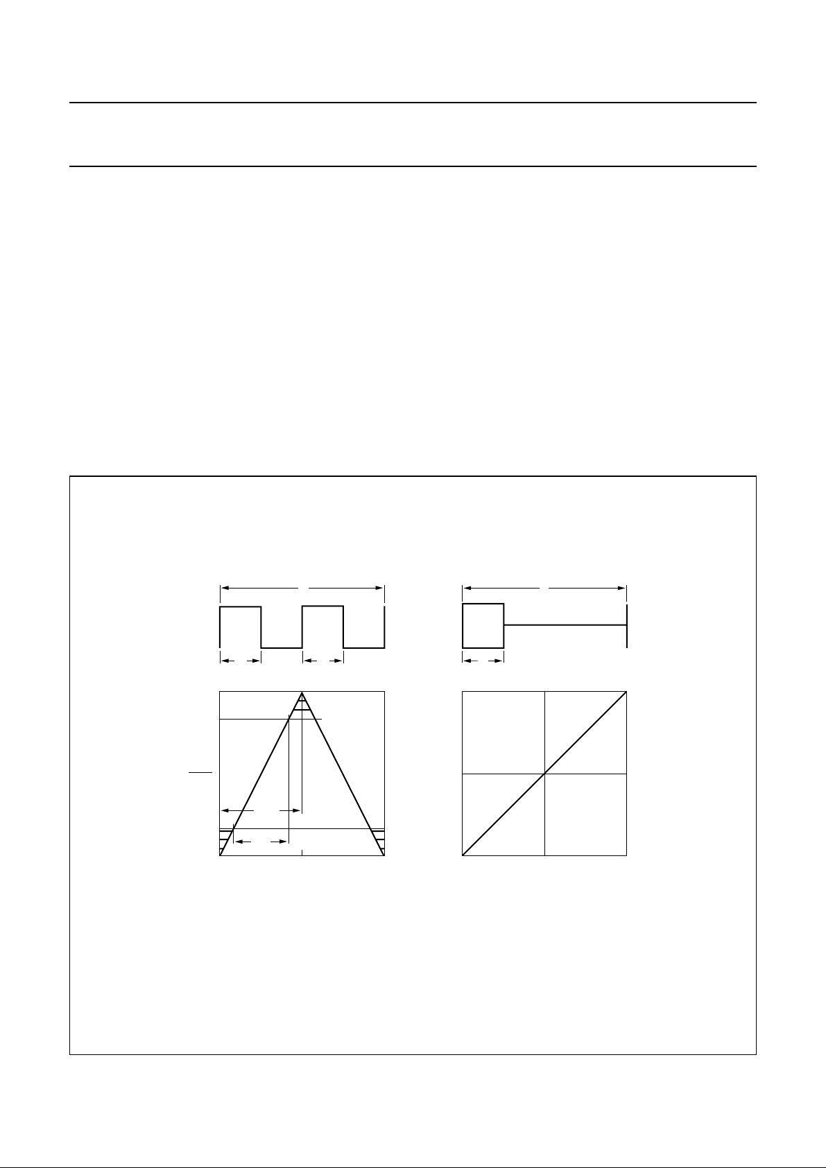
7.2.3.1 XOR mode
PHDIF is the XOR function of SIG and REF. The frequency
is twice the frequency of SIG and REF. The PHDIF output
carries a signal, switching between GND and VDD, with an
average value V
which is a function of the phase
avg
difference between SIG and REF (see left part of Fig.6).
The locking range in this mode of operation is maximum
for even values of N3 (180 degrees phase difference) but
less for odd values of N3. It is minimum for N3=3
(120 degrees phase difference).
7.2.3.2 Edge triggered mode
PHDIF is only influenced by the rising edges of SIG and
REF. Consequently its frequency is equal to the SIG and
REF frequency.
handbook, full pagewidth
T
The electrical behaviour of the PHDIF output pin in this
mode is special:
PHDIF is HIGH from the rising edge of REF to the rising
edge of SIG and 3-stated elsewhere if REF is leading and
PHDIF is low from rising edge of SIG to rising edge of REF
and 3-stated elsewhere if REF is trailing. Therefore PHDIF
is NOT 3-stated during a portion t
acts as a pull-up device or during a portion t
of each cycle when it
up
of each
down
cycle when it acts as a pull-down device (see right part of
Fig.6).
As a result the locking range is always 360 degrees phase
difference. The output behaviour as function of phase
difference is non-symmetrical with reference to the vertical
axis, but a reversed mode is also available (by setting the
control flag PHSRVS).
T
PHDIF
t
1
t
2
t
3-stated
XOR mode edge triggered mode
1
5/6
V
avg
V
DD
max
1/6
0
min
o
0
REF to SIG phase difference
180
o
360
o
100%
t
up
t
down
100%
0%
o
−180
REF to SIG phase difference
o
0
+180
MGE473
o
Fig.6 PHDIF output behaviour.
1997 Nov 17 10

Philips Semiconductors Preliminary specification
ISO/MPEG Audio Source Decoder SAA2502
7.2.4 LIMITED SAMPLING FREQUENCY SUPPORT FOR
INTERNAL SAMPLING CLOCKS
7.2.4.1 When sampling frequency is limited to
44.1 and/or 22.05 kHz:
In this event MCLKIN is only required to generate the
master clock frequency. Consequently the remarks on
MCLKIN frequency also apply in this special case.
7.2.4.2 When sampling frequency is limited to
48, 32, 24 and/or 16 kHz:
In this event X22IN is not required. Therefore X22IN
should be connected to VSS or VDD, but it is more efficient
to apply any available clock signal to X22IN. Because
44.1 kHz is the default initial sampling frequency it may
also be advisable to over-rule the sampling frequency after
a hard reset.
7.3 Input interface module
The input interface module handles the reception of the
coded input data stream.
The module can be configured to operate in 3 distinct
modes of operation:
• The master input mode
• The slave input mode
• The buffer controlled input mode.
Input interface mode must be stationary while the device is
in normal operation. Changing mode will result in an
(automatically generated) internal soft reset.
CDRQ changes at the falling edge of CDCL.
CDVAL = logic 0 indicates that CD and CDEF should be
ignored while CDVAL = logic 1 indicates that CD is a valid
coded input stream data bit (CDEF is then its error
attribute).
CDEF = logic 0 means that the value of CD may be
assumed to be reliable while CDEF = logic 1 means that
the value of CD is flagged as insecure (e.g. due to erratic
non-correctable channel behaviour). The value of CDEF
may be different for each data bit, but is combined by the
SAA2502 for every group of 8 (byte aligned) valid coded
input bits.
CDSY will only have effect when the SYMOD control flags
are set to 10 or 11. When SYMOD = 10 the valid input bit
at a rising edge of CDSY marks the start of a new byte
(when SYMOD = 11 it marks the start of a new MPEG
audio frame). Note that just the rising edge of CDSY is
important, the falling edge has no meaning.
If CDSY is used with SYMOD = 10 leading edges must be
frequent enough to assure fast byte alignment, if used with
SYMOD = 11 a leading edge must be present every frame.
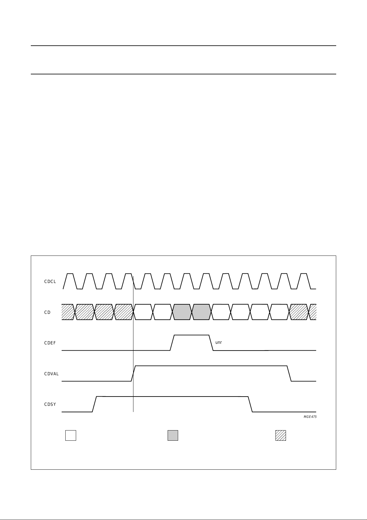
Leading edges of CDSY may occur while CDVAL is
(implicitly) high. Alternatively, a situation as shown in Fig.8
is also allowed, where CDSY has a rising edge while
CDVAL is low, i.e. during invalid data. The first valid CD bit
after the rising edge of CDVAL is then interpreted as the
first byte or frame bit.
The output pin CDRQ is used to request new coded input
data.
The inputs CD, CDVAL, CDEF and CDSY are all clocked
at the rising edge of the CDCL bit clock.
Table 4 Signals of coded data input interface
SIGNAL DIRECTION FUNCTION
CD input coded data input bit
CDVAL input coded data bit valid flag
CDEF input coded data bit error flag
CDSY input coded data sync (start of byte/frame) indication
CDCL input/output coded data bit clock
CDRQ output coded data request
1997 Nov 17 11
Philips Semiconductors Preliminary specification
,,
ISO/MPEG Audio Source Decoder SAA2502
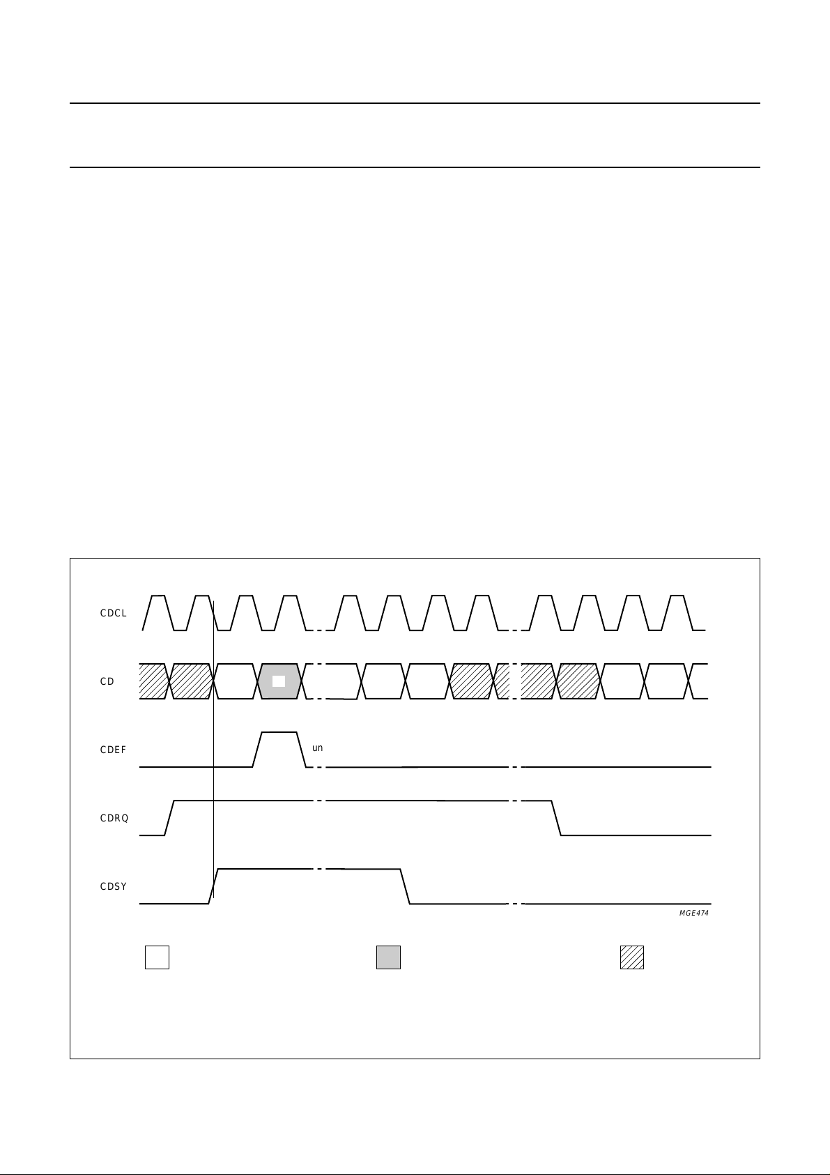
7.3.1 MASTER INPUT MODE
Master input mode is the default mode of operation. This
mode may also be enforced by setting the INMOD control
flags to 00. Which means that the SAA2502 will generate
requests for input data at regular intervals. CDVAL is not
used in this mode (it should be connected to VSS or VDD).
CDVAL is implicitly assumed to be logic 1 during the 2nd
up to (and including) the 17th bit slot after a rising or a
falling edge of CDRQ (see Fig.7). Thus signal CD should
carry the coded data in bursts of 16 valid bits.
In this mode the CDRQ frequency is locked to (i.e. derived
from) the 256 × f
clock. Its average value equals the bit
s
rate divided by 32.
The bit clock CDCL is output, its frequency is fixed:
MCLK
----------------- -
MCLK
----------------- -
handbook, full pagewidth
when MCLK24 = logic 1
32
when MCLK24 = logic 0.
16
CDCL
MPEG free format bit rate is NOT allowed in this mode.
Assume N is the number of CDCL periods between two
transitions of CDRQ, and R is the number of CDCL periods
to obtain the effective bit rate E (in kbits/s) at a CDCL
frequency of 768 kHz, i.e. .
R
16 768×
=
---------------------E
The SAA2502 keeps the average value of N exactly at R,
but individual values of N may vary between
N = round (R) −2 and N = round (R) +2.
7.3.2 S
LAVE INPUT MODE
Slave input mode is activated by setting the INMOD control
flags to 0 1. Which means that the SAA2502 will accept
input data as presented by the application. In this mode it
is the responsibility of the application to maintain locking
between the 256 × fs sample clock and the average bit
rate.
CD
CDEF
CDRQ
CDSY
start of byte or frame
valid data
1 1 22
15
14
unreliable data bit (example)
16
valid but unreliable data
Fig.7 Master mode input data format.
MGE474
invalid data
1997 Nov 17 12
Philips Semiconductors Preliminary specification
ISO/MPEG Audio Source Decoder SAA2502
The bit clock CDCL is input, its frequency is determined by
the application, however certain minimum and maximum
values have to be obeyed.
MPEG free format bit rate is allowed in this mode.
CDVAL = logic 1 indicates valid data. In this way, burst
input data is supported.
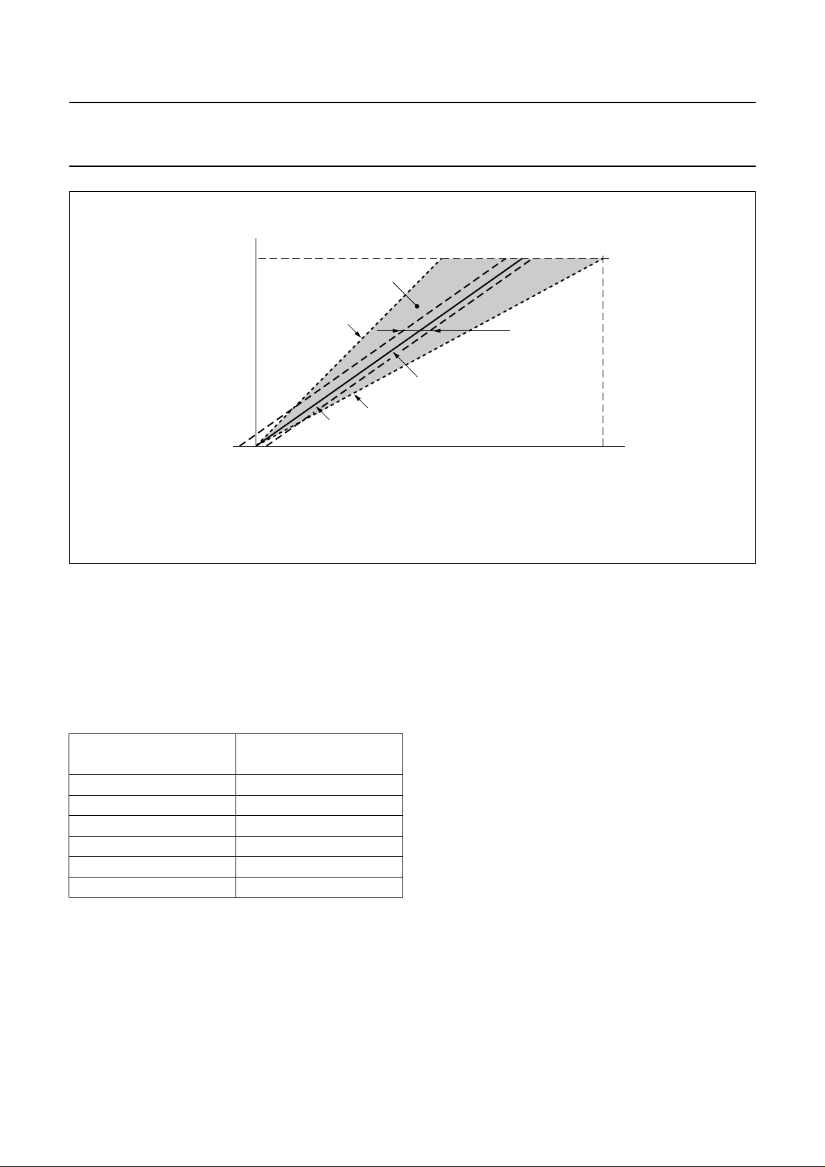
The speed at which data may be transferred to the input
interface is restricted. Transfer of an MPEG frame is
illustrated in Fig.9. It shows the transfer of all Nf bits of one
frame between time 0 and Tf, where Tf corresponds to
384 sample periods (MPEG layer I input data) or
1152 sample periods (MPEG layer II input data). In the
figure, an example of an actual transfer characteristic is
drawn. Input data may be transferred at a speed higher
than bit rate (i.e. CDCL may have a frequency higher than
bit rate).
Ideally the data transfer of the first frame is in a single
burst. In practice multiple bursts are allowed, provided that
the data transfer is always within ±128 CDCL cycles of the
ideal data transfer.
Subsequent frames may also have multiple bursts, but the
data transfer must always be within ±128 CDCL cycles of
both the first frame data transfer and the ideal single burst
transfer characteristics. All frames must start within the
first four bytes of a data burst.
The transfer characteristic has a slope equal to CDCL
frequency during the bursts (when CDVAL is high) and is
horizontal outside the bursts (when CDVAL is low; no bits
are transferred). The frequency of CDCL has to be
constant (except when CDVAL is low) in normal operation;
any change of CDCL frequency should be followed by a
(soft) reset.
For DAB applications there is an exception to the rule that
data transfer is always within ±128 CDCL cycles of the
ideal single burst characteristic.
When the sampling frequency is 24 kHz and the CDCL
frequency is 384 kbits/s, it is allowed to send an input
frame in two bursts of equal length. The first bit of a frame
must be the first bit of a burst, while the last bit of a frame
must be the last bit of a burst.
handbook, full pagewidth
CDCL
CD
CDEF
CDVAL
CDSY
valid data
start of byte or frame
unreliable data bits (example)
valid but unreliable data
MGE475
invalid data
Fig.8 Slave mode input data format.
1997 Nov 17 13
Philips Semiconductors Preliminary specification
ISO/MPEG Audio Source Decoder SAA2502
handbook, full pagewidth
Nf
(1)
transferred
input bits
0
(1) Ideal frame transfer characteristics are restricted to this area.
(2) Ideal frame transfer characteristic (example).
slope = maximum
CDCL frequency
0
slope = input bit rate
(2)
Fig.9 Slave input data transferring speed.
The shaded area in Fig.9 represents the restrictions to the
transfer characteristic of a frame. The characteristic may
not cross the shown upper limit of the shaded area in order
to prevent input buffer underflow and/or overflow.
The slope of the upper limit is determined by the sample
frequency as shown in Table 5.
jitter limits
slope = CDCL frequency
time
MGE476
Tf
Table 5 Slope of the upper limit determined by sampling
frequency
SAMPLE FREQUENCY
(kHz)
MAXIMUM CDCL
FREQUENCY (kbits/s)
48 768
44.1 705.6
32 512
24 384
22.05 352.8
16 256
1997 Nov 17 14
Philips Semiconductors Preliminary specification
ISO/MPEG Audio Source Decoder SAA2502
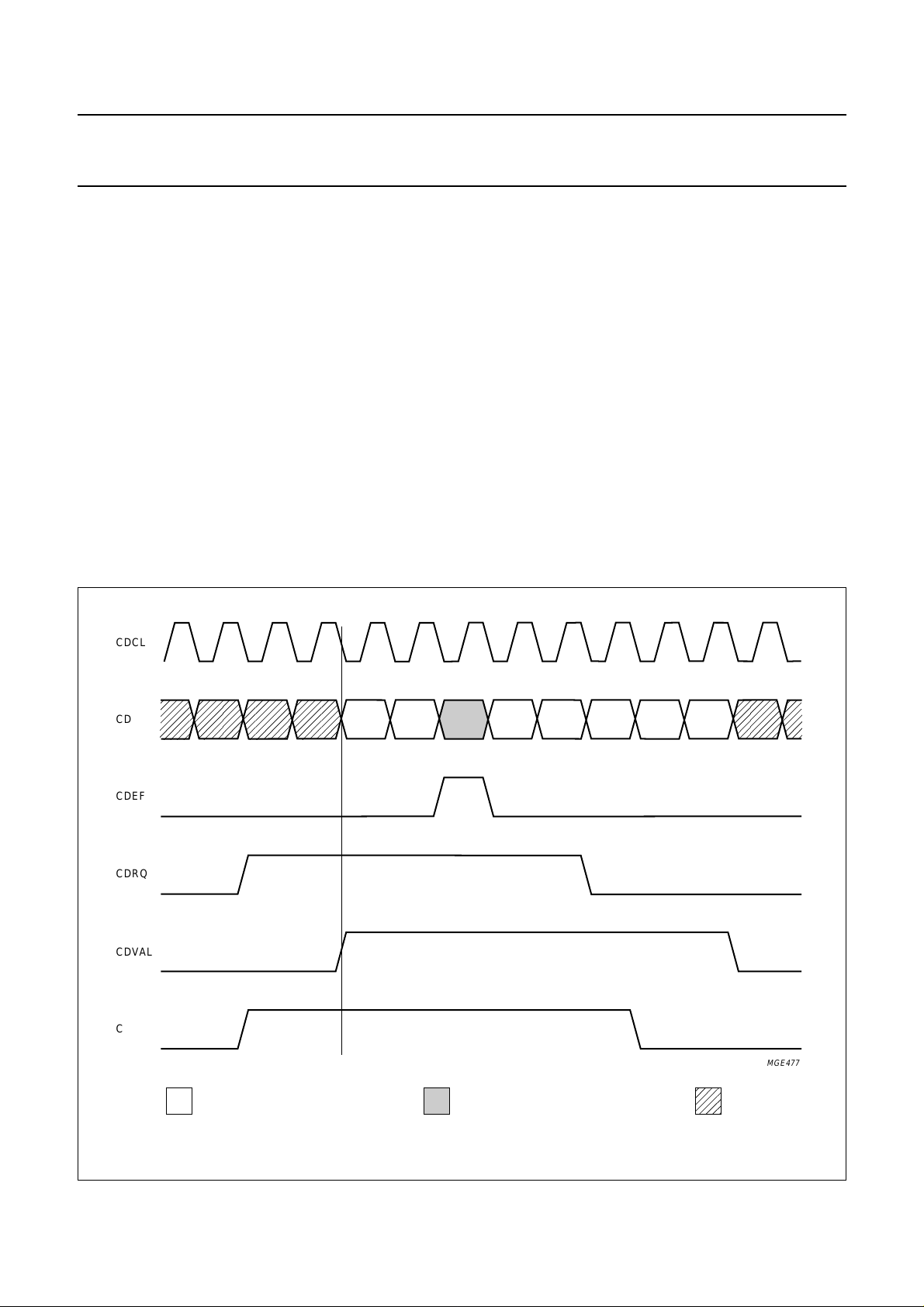
7.3.3 BUFFER CONTROLLED INPUT MODE (see Fig.10)
Buffer controlled input mode is activated by setting the
INMOD control flags to 1X, which means that the SAA2502
will request data based on the amount of input bytes
currently residing in the input buffer.
The bit clock CDCL is output, its frequency is fixed:
MCLK
----------------- -
MCLK
----------------- -
when MCLK24 = logic 1
32
when MCLK24 = logic 0.
16
In this mode CDRQ = logic 1 is an indication that new input
data is required. CDVAL = logic 1 indicates the delivery of
valid data. The application should react to the event of an
input data request as follows:
• One byte of input data should be delivered within
16 CDCL cycles. If CDRQ remains high the next byte
handbook, full pagewidth
CDCL
should be delivered and so on until CDRQ is dropped.
Delivery of subsequent bytes while CDRQ remains
HIGH should be uninterrupted (CDVAL should stay
HIGH)
• There is also an option for the application to deliver part
of the input data later. Despite violating the conditions in
the previous paragraph, this is allowed, but with
consequences for the input buffer latency time.
MPEG free format bit rate is allowed in this mode.
Dynamically varying bit rate may be supported in this
mode. Whether such support is desired or not is indicated
by the following input mode bits:
• INPMOD = 10 means bit rate is assumed to be (quasi)
static
• INPMOD = 11 means bit rate is assumed to be dynamic.
CD
CDEF
CDRQ
CDVAL
CDSY
valid data
unreliable data bit (example)
start of byte or frame
valid but unreliable data
Fig.10 Buffer controlled mode input data format.
MGE477
invalid data
1997 Nov 17 15

Philips Semiconductors Preliminary specification
ISO/MPEG Audio Source Decoder SAA2502
7.4 Decoder core
The SAA2502 fully complies with MPEG1 (layer I and II)
and MPEG2 (layer I and II, L0 and R0 channels). Also
some DAB specific features are supported. Free format bit
rate is not supported in master input mode. Several
aspects of the decoding process and audio
post-processing features are offered.
7.4.1 F
The SAA2502 has to localize the start of a frame before
decoding may begin. The process of locating the start of a
frame is called frame synchronization. There are
4 different modes of frame synchronization available.
These modes are in order of decreasing speed of frame
synchronization.
RAME SYNCHRONIZATION TO INPUT DATA STREAMS
7.4.1.1 Frame sync pulse mode
In this mode the start of each frame is marked by a rising
edge of the CDSY input pin. It is the fastest and most
reliable method of frame synchronization. It is activated by
loading 11 into the SYMOD control flags.
7.4.1.2 Byte aligned mode
This default mode may also be enforced by loading 10 into
the SYMOD control flags. The start of a frame is located by
detection of the 14-bit sync pattern 111111111111X1.
The probability of correct sync detection is enhanced by
the fact that a rising edge of the CDSY input pin marks a
location which is byte aligned with frame bounds. A rising
edge of CDSY is not required at every byte edge but
should occur at regular intervals for reliable frame
synchronization.
7.4.1.3 Layer II non-byte aligned mode
This mode may be entered by loading 01 into the SYMOD
control flags. Frame start is found by detection of the 15-bit
sync pattern 111111111111X10.
As this pattern is slightly longer than the previous one and
also contains at least one 1-to-0 transition, it may be used
to obtain frame synchronization in the absence of any
external alignment indication (CDSY is ignored and
therefore may be left floating).
7.4.1.4 General non-byte aligned mode
This mode may be entered by loading 00 into the SYMOD
control flags. Frame start is detected by alternating
searches for a 15-bit sync pattern 111111111111X10
(identical to the layer II mode search pattern) and a15-bit
sync pattern 0111111111111X1.
Because valid MPEG streams exist that do not contain the
first pattern while other valid MPEG streams do not contain
the second pattern a time-out counter will always be active
in this mode. Time-out length is set to slightly more then
72 ms which is the length of the longest audio frame.
The second pattern operates for layer I and layer II, but
successful synchronization is only guaranteed when the
last bit of the previous frame equals logic 0. Consequently
this mode synchronizes to layer I input bit streams only if
frames at least sometimes end with a logic 0 bit. Both
patterns contain the 1-to-0 or 0-to-1 transition required for
a reliable start-of-frame detection in the absence of
external alignment information.
If the SAA2502 starts at a random place in the bit stream,
it may take up to one frame before a sync pattern or sync
pulse is encountered. Because sync patterns may be
emulated by frame content, detection of a sync is always
followed by a verification period to check whether the sync
is located at the start of a frame. The length of the
verification period depends on the presence of CRC
protection and/or a free format bit rate index. During sync
search and verification the baseband audio outputs are
muted. If verification fails the synchronization process is
restarted.
Table 6 Frame sync verification
INPUT DATA FORMAT
FREE FORMAT BIT RATE NON-FREE FORMAT BIT RATE
MPEG; no CRC 2 frame bit rate 1 frame
MPEG with CRC 1 frame 0 frame
1997 Nov 17 16
LENGTH OF VERIFICATION PERIOD
Philips Semiconductors Preliminary specification
ISO/MPEG Audio Source Decoder SAA2502
7.4.2 MASTER INPUT MODE BIT RATE GENERATION
When master input mode is used, the SAA2502 fetches
input data at the effective bit rate. However after a hard
reset the input requests input data at the default bit rate
until synchronization has been established as shown in
Table 7.
When the clock generator mode is ‘free running internal
sample clock’ or ‘locked internal sample clock’ the default
input bit rate is always 384 kbits/s. When the mode is
‘external sample clock’ the SAA2502 derives the selected
bit rate from the signal FSCLKIN. But initially it has no
indication of the current sampling rate corresponding to
FSCLKIN. Therefore the bit rate of 384 kbits/s is
generated at an assumed sampling frequency of 44.1 kHz.
For different sample rates, the bit rate changes
proportionally.
The consequence is that while the SAA2502 is
synchronizing after a hard reset, the application should be
able to supply input data at the given default bit rate until
synchronization is established. Alternatively there is also
the possibility to overrule default bit rate setting and
sample rate setting using the control interface while
synchronization has not been established.
The speed at which input data is requested by the input in
master mode is changed in one of the following events:
• When input synchronization is established at the end of
the verification phase and the bit rate index of the
decoded bit stream indicates a bit rate different from the
one currently selected. In this event, the bit rate is
adapted to the new index.
• When the signal STOP is raised while the STOPRQ
control flag = logic 1, input requesting is halted.
Requesting resumes at the last selected input bit rate
when the STOP signal is dropped.
In all other events (including when the SAA2502 loses
synchronization), the last selected input bit rate is
maintained.
Whenever the selected bit rate changes while dynamic bit
rate is not enabled, the SAA2502 will generate internally a
soft reset resulting in a soft mute of the output interfaces
and a decoder restart in order to re-initialize internal buffer
settings.
Table 7 Establishment of default bit rate
CLOCK GENERATOR MODE FSCLKIN (kHz) DEFAULT BIT RATE (kbits/s)
Free running internal clock don’t care 384
Locked internal clock don’t care 384
External sample clock 256 or 384 × 48 417.96
256 or 384 × 44.1 384
256 or 384 × 32 278.64
256 or 384 × 24 208.98
256 or 384 × 22.05 192
256 or 384 × 16 139.32
1997 Nov 17 17
Philips Semiconductors Preliminary specification
ISO/MPEG Audio Source Decoder SAA2502
7.4.3 SAMPLE CLOCK GENERATION
When the ‘external sample clock’ mode of the clock
generator is used, the application must know the sample
rate. FSCLKIN has to be applied, with a frequency which
is a multiple of the sample rate. The (sample rate
dependent) output interface timing signals will be
generated from FSCLKIN. This mode will normally be
used in applications with a fixed sample rate. Should the
sample rate change, then a soft reset is strongly advised.
When one of the remaining clock generator modes is used,
the SAA2502 selects the active sample rate automatically,
and generates the required sample rate related timing
signals from its MCLKIN and X22IN clock inputs. Soft
resets at sample rate changes are generated
automatically. After a hard reset, a sample rate of 44.1 kHz
by default is selected. Such default setting may be
overruled using the control interface.
SCK, WS and SPDIF will show frequency changes in any
of the following 3 situations:
• When the SAA2502 establishes synchronization to the
coded data input bit stream at a sample rate different
from the one previously selected
• When the current (default) sample rate is overruled by
the control interface
• When the clock generator mode is changed, resulting in
a switch from or to the ‘external sample clock mode.
7.4.4 DECODER PRECISION
During decoding several multiply operations are carried
out on coded samples. The results of these operations
have to be rounded in order to keep the word length
required for internal number representation within
reasonable limits. Accumulation of these rounding errors is
kept at a very low level in order to assure precise audio
output samples. SAA2502 precision is specified using the
output of the MPEG reference decoder based on double
precision floating point calculations as a reference.
Differences between that reference decoder and SAA2502
output manifest themselves as white noise.
Two contributions to this noise may be identified:
• Noise resulting from internal rounding on intermediate
results
• Noise resulting from rounding of final output samples
to 16, 18, 20 or 22 bits (depending on selected output
accuracy).
Table 8 shows the effective noise level figures. (unit is
1 LSB of 22-bit accuracy output). Except for 22-bit
accuracy, output rounding is by far the dominant effect.
Consequently the SAA2502 may be considered a
professional level high precision decoder.
In all those situation the phase of WS and the data content
of SPDIF will be continuous.
In all other events SCK, WS and SPDIF remain operating
without phase or frequency changes and the sample rate
selection remains unchanged.
Table 8 Effective noise level figures
OUTPUT ACCURACY
(BITS)
22 0.6 0.3 0.7
20 0.6 1.2 1.3
18 0.6 4.6 4.7
16 0.6 18.5 18.5
Note
1. The output rounding part of this precision is valid only for I2S and SPDIF outputs.
INTERMEDIATE
ROUNDING
OUTPUT ROUNDING
(1)
TOTAL NOISE LEVEL
1997 Nov 17 18

Philips Semiconductors Preliminary specification
ISO/MPEG Audio Source Decoder SAA2502
7.4.5 SCALE FACTOR CRC PROTECTION
MPEG specifies an optional 16 bit CRC that may be used
to verify whether an important part of each audio frame is
received correctly. The following data items is protected by
this CRC:
• Bytes 3 and 4 of the first 4 bytes of each frame,
containing most of the frame header information
• Allocation information
• Scale factor select information (layer II only).
The scale factors are not protected by this scheme.
The DAB specification includes CRC protection for scale
factors. The 32 sub-bands are divided into the following
4 blocks:
Block 0 = sub-bands 0 to 3
Block 1 = sub-bands 4 to 7
Block 2 = sub-bands 8 to 15
Block 3 = sub-bands 16 to 31.
Each block is protected by an 8-bit CRC if that block of
sub-bands is (partly) inside the current sub-band limit.
The required scale factor CRCs are stored in the last bytes
of the previous audio frame:
• The last two bytes of each frame are reserved for
ancillary data; DAB specification calls this Fixed
Program Associated Data (FPAD)
• Minimum 2 and maximum 4 bytes before FPAD are
reserved for scale factor CRCs. The number of CRC
bytes present is be derived from the sub-band limit of the
following audio frame
• Bytes before the CRCs are available for more ancillary
data; DAB specification calls this extended Program
Associated Data (XPAD), as far as not occupied by
MPEG coded input data.
7.4.6 HANDLING OF ERRORS IN THE CODED INPUT DATA
The SAA2502 is able to handle certain types of errors in
the input data. Three error categories will be handled:
• Errors flagged by the coded input data error flag CDEF
• CRC failures (if MPEG and/or scale factor error
protection is active)
• MPEG audio frame syntax errors.
Error flags in the input data will effect the decoding process
if the corrupted data is inside the header, bit allocation or
scale factor select information part of a frame (then the
SAA2502 will ‘soft’ mute that frame) or inside the scale
factor field (then the most recent valid scale factor of the
same sub-band will be copied).
Error flags in other data fields will be ignored. If MPEG
and/or scale factor CRCs are active the CRC result has
priority over CDEF flags inside the protected fields. In
applications where the MPEG CRC is always present, the
protection bit (which is not CRC protected) in the MPEG
header may be overruled by setting control flag CRCACT.
Thus the SAA2502 is robust for data errors in the
protection bit.
The DAB type of scale factor CRC protection, extended to
all valid sample frequency plus bit rate combinations of
MPEG1 and MPEG2, and to layer I, is fully supported by
the SAA2502. (DAB is restricted to MPEG1 layer II, to
48 kHz sample frequency and does not support free
format bit rate). Requirements for scale factor CRC
handling is indicated by the SFCRC control flag.
1997 Nov 17 19
Philips Semiconductors Preliminary specification
ISO/MPEG Audio Source Decoder SAA2502
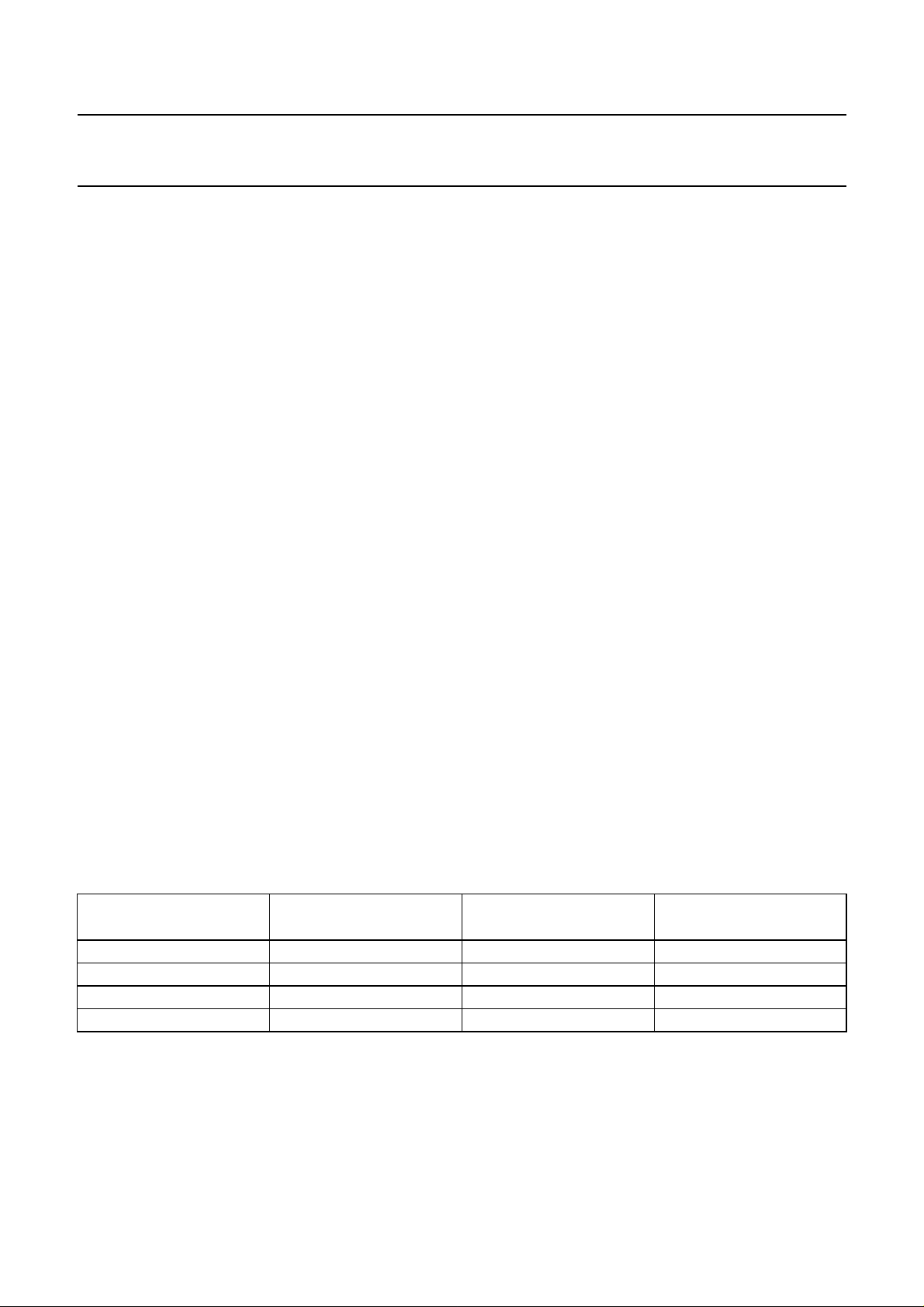
7.4.7 DYNAMIC RANGE COMPRESSION
The baseband audio output resulting from MPEG
decoding has a high dynamic range (theoretically
>200 dB, practically up to 120 dB for the 22-bit output
mode).This feature is very attractive from the high quality
audio standpoint of view, but such high dynamic range is
undesirable when there is a relatively high level of
background noise (e.g. for car radio). For those
applications the SAA2502 offers the possibility of built in
dynamic range compression:
• Internal dynamic range compression is offered. Thus
any standard MPEG encoded bit stream may be
compressed i.e. no added compression information is
required.
• The dynamic range compression algorithm is fully
parameterised. All major characteristics are
programmable through the control interface:
– Level of compression
– Maximum compression
– Compression offset
– Compression release rate (compression attack rate
has to be fixed).
The dynamic range compression algorithm is based on a
(in time varying) amplification factor, which is equally
applied to all audio output samples. The value of the
amplification factor is calculated on basis of the current
audio output power level for each (sub)frame of 384 output
samples. The applied power to amplification curve is
shown in Fig.11. All characteristics of the curve are
programmable:
• Compression slope minimum = 0, maximum = 0.996
• Maximum amplification minimum = 0 dB,
maximum = 23.81 dB
• Offset minimum = 0 dB, maximum = 47.81 dB.
Offset values close to 0 dB may result in clipped output
signals. This is especially true for signals with a high
amplitude-to-power ratio (an extreme example of such a
signal is a maximum amplitude unit impulse).
The occurrence of this effect can be avoided by selecting
an offset value close to or greater than 15 dB.
In the context of dynamic range compression definition,
the 0 dB power reference level is defined as a sine wave
shaped output signal with maximum amplitude in just one
(right or left) channel.
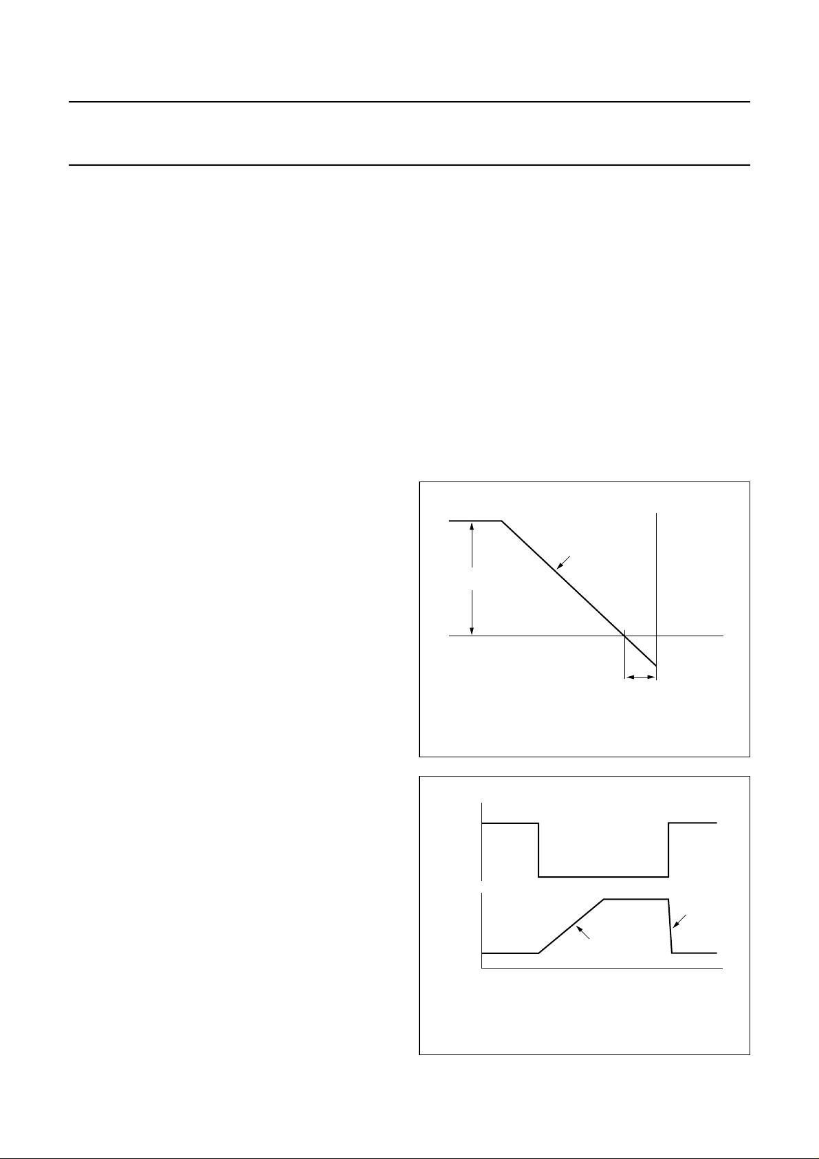
The calculation will result in an new amplification factor
every 384 samples (i.e. from 8 ms at 48 kHz to 24 ms at
16 kHz sample rate). Subsequent amplification factors
may vary considerably.
An example showing two large step type discontinuation is
shown in Fig.12. It is undesirable to apply large increasing
amplification steps immediately. Consequently increasing
the amplification factor is limited to the ‘release rate’ which
is also programmable:
• Minimum release rate =
0.0117 dB
---------------------------------384 samples
(1.46 dB/s at 48 kHz; 0.488 dB/s at 16 kHz)
• Maximum release rate =
0.375 dB
---------------------------------384 samples
(46.87 dB/s at 48 kHz; 15.625 dB/s at 16 kHz).
Decreasing amplification factors, must be applied almost
immediately to avoid overflow when the audio power
increases rapidly; thus attack rate is non-programmable
and fast.
handbook, halfpage
maximum
amplification
compression
slope
offset
amplification
(dB)
0 dB
power (dB)
MGE478
Fig.11 Dynamic range compression characteristic.
handbook, halfpage
audio
signal
power
amplifi-
cation
release
rate
MGE479
attack
rate
time
Fig.12 Amplification change rates.
1997 Nov 17 20
 Loading...