

Philips SAA2501H Datasheet

INTEGRATED CIRCUITS
DATA SH EET
SAA2501
Digital Audio Broadcast (DAB)
decoder
Preliminary specification
File under Integrated Circuits, IC01
Philips Semiconductors
January 1995

Philips Semiconductors Preliminary specification
Digital Audio Broadcast (DAB) decoder SAA2501
CONTENTS
FEATURES
2 APPLICATION
3 GENERAL DESCRIPTION
4 ORDERING INFORMATION
5 BLOCK DIAGRAM
6 PINNING
7 FUNCTIONAL DESCRIPTION
7.1 Coding system
7.2 Basic functionality
7.3 SAA2501 clocks
7.4 Crystal oscillator
7.5 Clock frequencies when using the slave input
7.6 Clock frequencies when using the master input
7.7 Target applications; applying the SAA2501 with
2 ISO/MPEG sources
7.8 Buffered clock outputs
7.9 Functionality issues
7.10 Synchronization to input data bitstreams
7.11 Master input bit rate selection
7.12 Sample rate selection
7.13 Handling of errors in the coded input data
7.14 sub-band filter signals
7.15 Baseband audio processing
7.16 Decoding control signals
7.17 Coded data interfaces
7.17.1 The coded data master input interface
7.17.2 The coded data slave input interface
7.17.3 Slave input transfer speed of first frame
7.17.4 Slave input transfer speed of subsequent
frames
7.18 The sub-band filter interface
7.19 The baseband output interface
7.20 The L3 control interface
7.20.1 L3 signals
7.20.2 L3 transfer types
7.20.3 L3 interface initialization at an SAA2501 device
reset
7.20.4 L3 interface control
7.20.5 SAA2501 status
7.20.6 Data items
7.20.6.1 General data items
7.20.7 SAA2501 settings item
7.20.8 Input data frame header items
7.20.9 Error report item
7.20.10 Audio service synchronized data item
7.20.11 Ancillary Data/XPAD item
7.20.12 APU coefficients item
7.20.13 Speed limitations of the L3 interface
7.20.14 Default item data values after reset
8 APPENDIX
8.1 Preliminary specification 3-line ‘L3’ interface
8.1.1 Introduction
8.1.1.1 Addressing mode
8.1.1.2 Special function operational address
8.1.1.3 Data mode
8.1.1.4 Halt mode
8.1.2 Device interface reset
8.1.3 Extended addressing
8.1.3.1 Operational address declaration
8.1.3.2 Operational address invalidation
8.1.4 Example of a data transfer
8.1.5 Timing requirements
8.1.5.1 Addressing mode
8.1.5.2 Data mode
8.1.5.3 Halt mode
8.2 SAA2501 L3 protocol enhancement options
8.2.1 Testing L3RDY by polling L3DATA
8.2.2 Options to increase the timing accuracy of the
APU coefficient writing
9 LIMITING VALUES
10 DC CHARACTERISTICS
11 AC CHARACTERISTICS
12 APPLICATION INFORMATION
13 PACKAGE OUTLINE
14 SOLDERING
14.1 Plastic quad flat-packs
14.1.1 By wave
14.1.2 By solder paste reflow
14.1.3 Repairing soldered joints (by hand-held
soldering iron or pulse-heated solder tool)
15 DEFINITIONS
16 LIFE SUPPORT APPLICATIONS
January 1995 2

Philips Semiconductors Preliminary specification
Digital Audio Broadcast (DAB) decoder SAA2501
1 FEATURES
• Advanced error protection
• Integrated audio post processing for control of signal
level and inter-channel crosstalk
• Demultiplexing of Program Associated Data (PAD) in
the input bitstream
• Automatic digital de-emphasis of the decoded
audio signal
• Separate master and slave inputs
• Automatic sample frequency and bit-rate switching in
master input mode
• Automatic synchronization of input and output interface
clocks in master input mode
• Selectable audio output precision; 16, 18, 20 or 22 bit
• Low power consumption
• Decoded sub-band signal and error flag outputs for error
concealment.
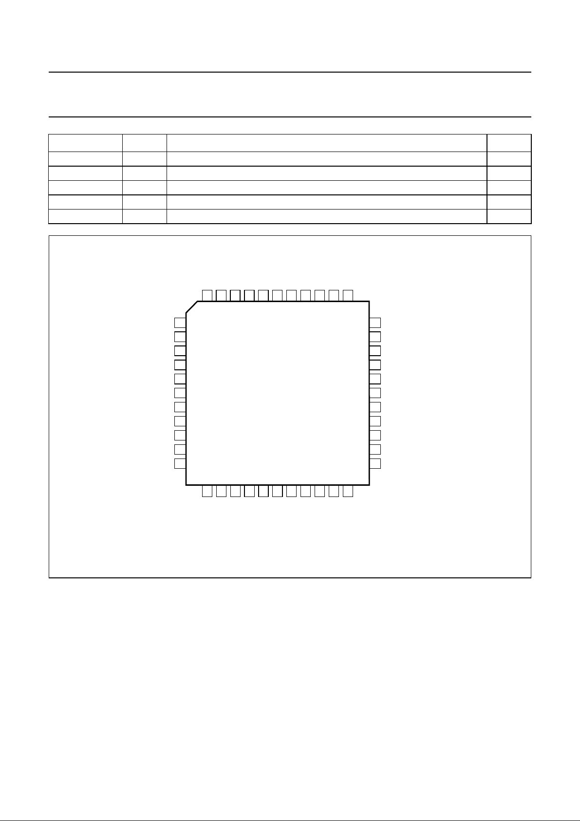
4 ORDERING INFORMATION
TYPE NUMBER
SAA2501H QFP44
NAME DESCRIPTION VERSION
(1)
plastic quad flat package; 44 leads (lead length 1.3 mm);
body 10 × 10 × 1.75 mm
2 APPLICATION
• Digital Audio Broadcast systems as defined in
“Eureka 147”
3 GENERAL DESCRIPTION
The SAA2501 audio source decoder supports ISO/IEC
MPEG layers I and II and all DAB specific features as
described in
PACKAGE
.
“Eureka 147 draft specification (EU147)”
SOT307-2
.
Note
1. When using IR reflow soldering it is recommended that the Drypack instructions in the
(order number 9398 510 63011) are followed.
Supply of this
right under any patent, or any Industrial or Intellectual Property Right, to use this IC in any ready-to-use
electronic product.
“ISO/IEC 11172-3”
audio standard Layer I or layer II compatible IC does not convey a licence nor imply a
“Quality Reference Handbook”
January 1995 3
Philips Semiconductors Preliminary specification
Digital Audio Broadcast (DAB) decoder SAA2501
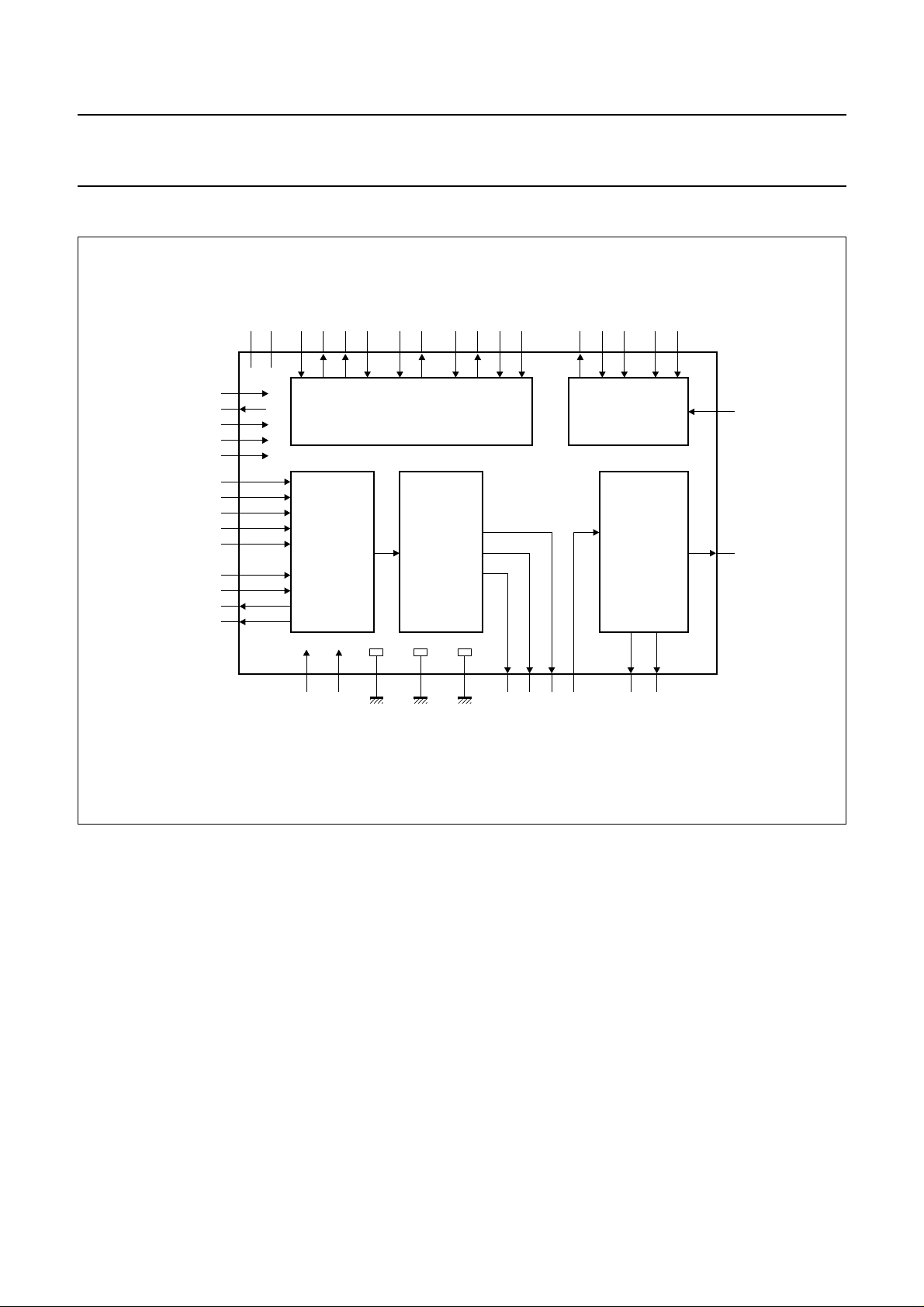
5 BLOCK DIAGRAM
handbook, full pagewidth
CDSEF
CDSCL
CDSWA
CDSSY
CDMEF
CDMCL
CDMWS
TDI
TDO
TCK
TMS
TRST
CDS
CDM
DD1
V
534
41
37
39
40
38
19
20
18
21
22
15
14
16
13
DD2
V
PROCESSOR
TC0 TC1
MCLK
MCLKIN
MCLKOUT
7444 10 9 3242 43 24 25 23 11 12
8
X22IN
MCLK24
CLOCK
GENERATOR
X22OUT
FSCLK
FSCLKIN
FSCLKM
FSCLK384
L3DATA
L3MODE
DECODING
CONTROL
L3CLK
SAA2501
SYNTHESYS
SUBBAND
FILTER
BANK
AND
OUTPUT
PROCESSING
SCK WS
FDAI
INPUT
36 35
PROCESSOR
17
GND2
DEQUANTI-
ZATION
AND
SCALING
GND3
6
GND1
FDEF
FDAO
FDFSY
URDA
STOP
1
RESET
26
SD
29 303231332728
MBE112
Fig.1 Functional block diagram.
January 1995 4

Philips Semiconductors Preliminary specification
Digital Audio Broadcast (DAB) decoder SAA2501
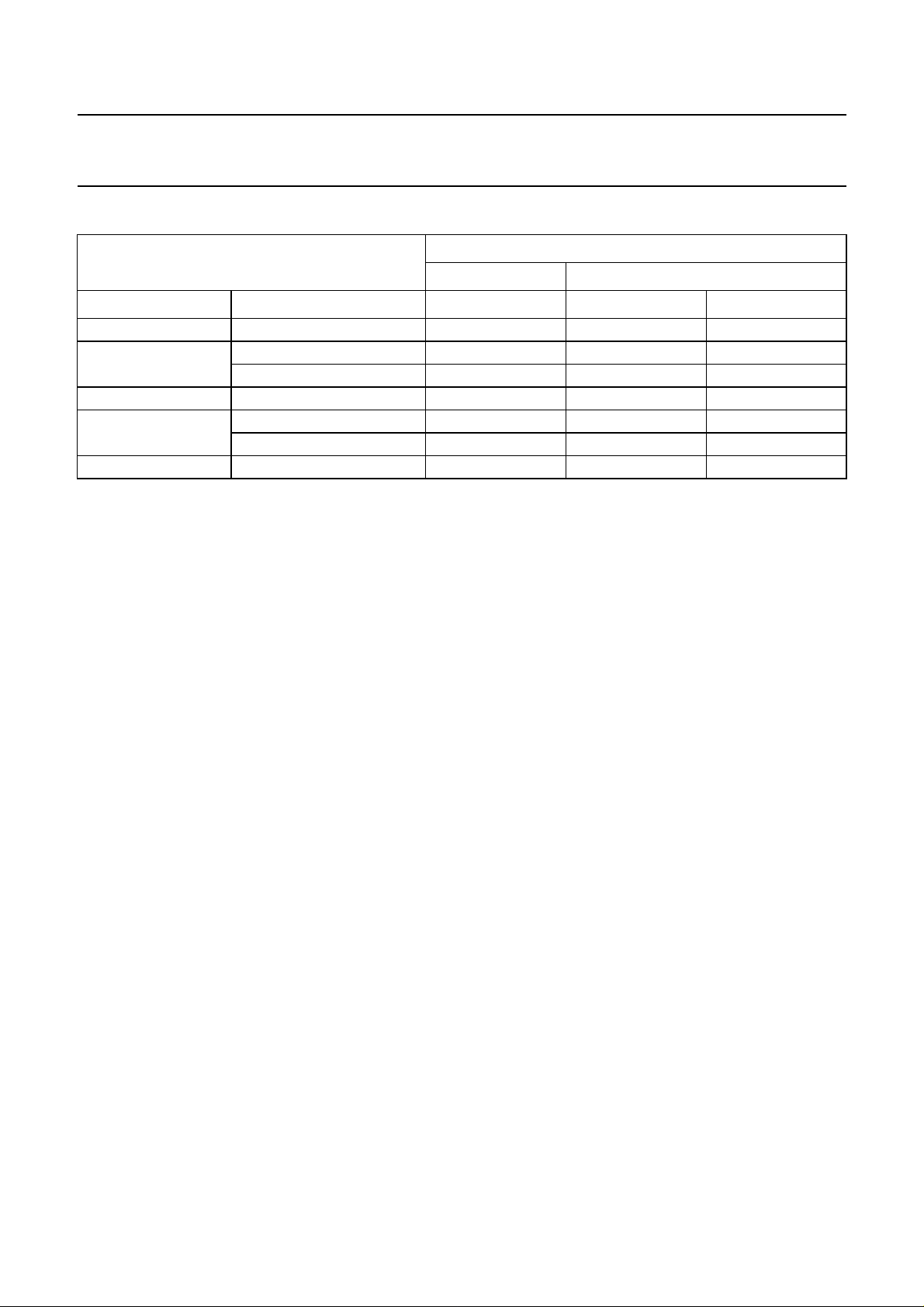
6 PINNING
SYMBOL PIN DESCRIPTION TYPE
RESET 1 master reset input I
FSCLK 2 sample rate clock output; buffered signal O
FSCLKIN 3 sample rate clock signal input (see Table 1) I
MCLK 4 master clock output; buffered signal O
V
DD1
GND1 6 ground 1 −
MCLKOUT 7 master clock oscillator output O
MCLKIN 8 master clock oscillator input or signal input I
X22OUT 9 22.579 MHz clock oscillator output O
X22IN 10 22.579 MHz clock oscillator input or signal input I
STOP 11 stop decoding input I
URDA 12 unreliable data input; interrupt decoding I
CDMWS 13 coded data (master input) word select output O
CDMEF 14 coded data (master input) error flag input I
CDM 15 ISO/MPEG coded data (master input) I
CDMCL 16 coded data (master input) bit clock output O
GND2 17 ground 2 −
CDSCL 18 coded data (slave input) bit clock I
CDS 19 ISO/MPEG or EU147 (see Table 8) coded data (slave input) I
CDSEF 20 coded data (slave input) error flag I
CDSWA 21 coded data (slave input) burst window signal I
CDSSY 22 coded data (slave input) frame sync I
L3CLK 23 L3 interface bit clock input I
L3DATA 24 L3 interface serial data input/output I/O
L3MODE 25 L3 interface address/data select input I
SD 26 baseband audio I
FDEF 27 filter data error flag output O
GND3 28 ground 3 −
SCK 29 baseband audio data I
WS 30 baseband audio data I
FDAO 31 filter data output O
FDAI 32 filter data input I
FDFSY 33 filter data output frame sync O
V
DD2
TC1 35 do not connect; factory test control 1 input, with integrated pull-down resistor I
TC0 36 do not connect; factory test control 0 input, with integrated pull-down resistor I
TDO 37 boundary scan test data output O
TRST 38 boundary scan test reset input; this pin should be connected to ground for
TCK 39 boundary scan test clock input I
5 supply voltage 1 −
2
S data output O
2
S clock output O
2
S word select output O
34 supply voltage 2 −
normal operation
I
January 1995 5
Philips Semiconductors Preliminary specification
Digital Audio Broadcast (DAB) decoder SAA2501
SYMBOL PIN DESCRIPTION TYPE
TMS 40 boundary scan test mode select input I
TDI 41 boundary scan test data input I
FSCLK384 42 sample rate clock frequency indication input I
FSCLKM 43 sample rate clock source selection for the master input I
MCLK24 44 master clock frequency indication input I
book, full pagewidth
RESET
FSCLK
FSCLKIN
MCLK
V
DD1
GND1
MCLKOUT
MCLKIN
X22OUT
X22IN
STOP
MCLK24
FSCLKM
FSCLK384
TDI
TMS
TCK
TRST
TDO
TC0
42
14
CDMEF
CDMWS
41
40
SAA2501
15
16
CDM
CDMCL
39
17
GND2
38
37
18
19
CDS
CDSCL
36
20
CDSEF
44
43
1
2
3
4
5
6
7
8
9
10
11
12
13
URDA
DD2
TC1
V
35
34
21
22
CDSSY
CDSWA
33
32
31
30
29
28
27
26
25
24
23
FDFSY
FDAI
FDAO
WS
SCK
GND3
FDEF
SD
L3MODE
L3DATA
L3CLK
MBE113
Fig.2 Pin configuration (QFP44).
7 FUNCTIONAL DESCRIPTION
7.1 Coding system
The perceptual audio encoding/decoding scheme defined
within the “
ISO/IEC 11172-3 MPEG Standard”
allows for a
high reduction in the amount of data needed for digital
audio whilst maintaining a high perceived sound quality.
The coding is based upon a psycho-acoustic model of the
human auditory system. The coding scheme exploits the
fact that the human ear does not perceive weak spectral
components that are in the proximity (both in time and
frequency) of loud components. This phenomenon is
called masking.
January 1995 6
For layers I and II of ISO/MPEG the broadband audio
signal spectrum is split into 32 sub-bands of equal
bandwidth. For each sub-band signal a masking threshold
is calculated. The sub-band samples are then
re-quantized to such an accuracy that the spectral
distribution of the re-quantization noise does not exceed
the masking threshold. It is this reduction of representation
accuracy which yields the data reduction. The
re-quantized sub-band signals are multiplexed, together
with ancillary information regarding the actual
re-quantization, into a MPEG audio bitstream.
Philips Semiconductors Preliminary specification
Digital Audio Broadcast (DAB) decoder SAA2501
During decoding, the SAA2501 de-multiplexes the MPEG
audio bitstream, and with knowledge of the ancillary
information, reconstructs and combines the sub-band
signals into a broadband audio output signal.
7.2 Basic functionality
From a functional point of view, several blocks can be
distinguished in the SAA2501. A clock generator section
derives the internally and externally required clock signals
from its clock inputs. The SAA2501 can switch between a
master and a slave input interface to receive the coded
input data. The input processor parses and de-multiplexes
the input data stream. The de-quantization and scaling
processor performs the transformation and scaling
operations on the sample representations in the input
bitstream to yield sub-band domain samples.
The sub-band samples are transferred via an external
detour to the synthesis sub-band filter bank processor.
The detour can be used to process the decoded audio in
the sub-band domain. The baseband audio samples,
reconstructed by the sub-band filter bank, can be
processed before being output.
The decoding control block houses the L3 control
interface, and handles the response to external control
signals. The L3 control interface enables the application to
configure the SAA2501, to read its decoding status, to
read Program Associated Data, and so on.
Several pins are reserved for Boundary Scan Test and
Scan Test purposes.
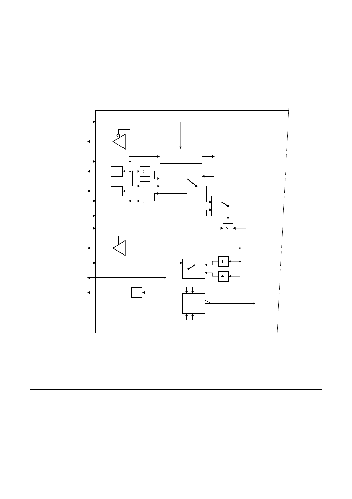
7.3 SAA2501 clocks
The SAA2501 clock interfacing is designed for application
versatility. It consists of 10 signals (see Table 1).
From a functional point of view, the clock generator inside
the device can be represented as shown in Fig.3.
As described above, the SAA2501 incorporates a master
input interface on which it requests for coded input data
itself, as well as a slave input interface for an imposed
coded data input bitstream. The input interface is selected
with flags MSEL0 and MSEL1, controlled via the L3
microcontroller interface.
Depending on the selected input interface, only a limited
number of the three possible input clocks (MCLKIN, X22IN
and FSCLKIN) is actually required. The various clock
options are selected with the 3 external control signals
MCLK24, FSCLKM and FSCLK384. These control signals
must be stationary while the device reset signal at
pin RESET is de-activated; changing any of these
3 signals without simultaneously resetting the SAA2501
can result in malfunctioning.
Table 1 Clock interfacing signals
SIGNAL DIRECTION FUNCTION
MCLKIN input master clock oscillator input or signal input
MCLKOUT output master clock oscillator output
MCLK output master clock output; buffered signal
MCLK24 input master clock frequency indication input:
MCLK24 = 0; MCLKIN frequency is 12.288 MHz (256 × 48 kHz)
MCLK24 = 1; MCLKIN frequency is 24.576 MHz (512 × 48 kHz)
X22IN input 22.5792 MHz (512 × 44.1 kHz) clock oscillator input or signal input
X22OUT output 22.5792 MHz (512 × 44.1 kHz) clock oscillator output
FSCLKIN input sample rate clock signal input
FSCLK output sample rate clock signal input; buffered signal
FSCLK384 input sample rate clock signal frequency indication input:
FSCLK384 = 0; FSCLKIN frequency is 256f
FSCLK384 = 1; FSCLKIN frequency is 384f
s
s
FSCLKM input sample rate clock source selection when using the master input:
FSCLKM = 0; use MCLKIN or X22IN as source
FSCLKM = 1; use FSCLKIN as source
January 1995 7
Philips Semiconductors Preliminary specification
Digital Audio Broadcast (DAB) decoder SAA2501
handbook, full pagewidth
MCLKOUT
FSCLKIN
FSCLK384
MCLK24
MCLK
MCLKIN
X22OUT
X22IN
FSCLKM
FSCLK
SCK
WS
control
12.288 or
24.576 MHz
OSC
OSC
22.5792 MHz
256f or 384f
s
control
control
64f
s
f
s
MCKDIS (L3)
s
FCKENA (L3)
64
in out
2
C = 48 kHz
C = 32 kHz
3
C = 44.1 kHz
2
CONTROL
DIVIDER
256f or 384f
s
C
internal master clocks
C
C = 0
C = 1
00
A
A=B
B
decoded sample rate index
256f
s
C = 0
C = 1
C
1
s
4
6
0: use master input
1: use slave input
to input
interfaces
MSEL1 MSEL0 (L3)
MGB491
Italics: internal signal designation.
Fig.3 SAA2501 clock generator.
7.4 Crystal oscillator
The recommended crystal oscillator configuration is shown in Fig.4. The specified component values only apply to
crystals with a low equivalent series resistance of <40 Ω.
January 1995 8
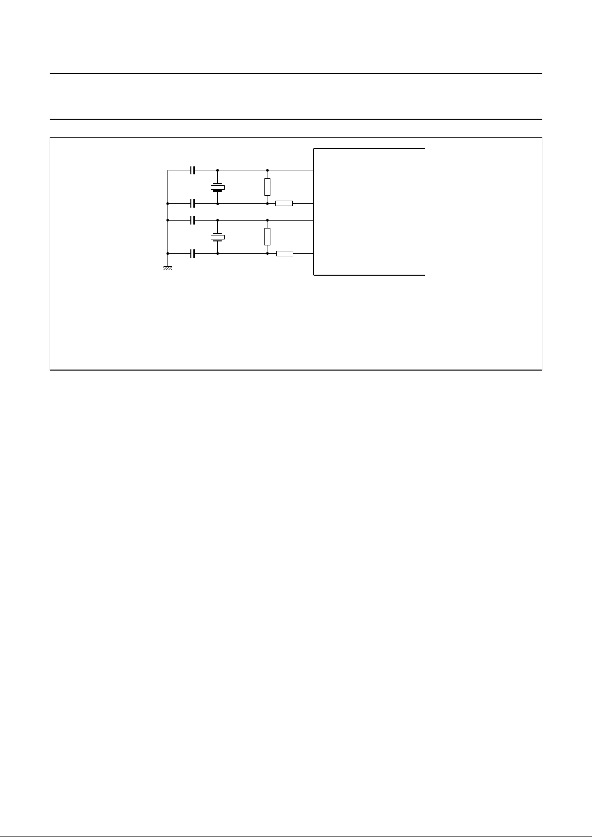
Philips Semiconductors Preliminary specification
Digital Audio Broadcast (DAB) decoder SAA2501
handbook, full pagewidth
C1 =C2 =33 pF;
R1=R4=1MΩ;
R2=R3=1kΩ;
X1 = 22.5792 MHz;
X2 = 24.5760 MHzor 12.2880MHz
The specified component values only apply to crystals with a low equivalent series resistance of <40 Ω.
C2
C1
C3
C4
X1
X2
R1
R4
R2
R3
10
9
8
7
Fig.4 Crystal oscillator components.
7.5 Clock frequencies when using the slave input
If the slave input is used (MSEL1 and MSEL0 = 10 or 11),
the SAA2501 clock sources are MCLKIN and FSCLKIN
and X22IN is not used. The I2S clocks SCK and WS are
generated by the SAA2501 from FSCLKIN. FSCLKIN may
be designated to have a frequency of 256 times (indicated
by FSCLK384 = 0) or 384 times (indicated by
FSCLK384 = 1) the sample frequency of the coded input
data. Master clock signal MCLKIN may be chosen to have
a frequency of 12.288 MHz (indicated by MCLK24 = 0) or
24.576 MHz (indicated by MCLK24 = 1). MCLKIN and
FSCLKIN do not have to be phase or frequency locked. If
the application is based on a sample frequency of 48 kHz
or 32 kHz, and a sample rate related clock of 12.288 MHz
(256 × 48 kHz; 384 × 32 kHz) is available, this can be
taken advantage of by using this signal for both MCLKIN
and FSCLKIN.
The main advantage of this configuration is that the
SAA2501 determines automatically which sample rate
is active from the sampling rate setting of the input
data bitstream, and then selects either MCLKIN or
X22IN as the clock source for the I
WS. This configuration is therefore particularly suited
in applications with more than one possible sample
rate setting.
2. If FSCLKM = 1, the configuration is comparable to the
configuration when using the slave input
(see Section 7.5). MCLKIN and FSCLKIN are used as
the clock sources, and X22IN is not required. MCLKIN
may again have a frequency of 12.288 MHz (indicated
by MCLK24 = 0) or 24.576 MHz (indicated by
MCLK24 = 1), and FSCLKIN may have a frequency of
256 times (indicated by FSCLK384 = 0) or 384 times
(indicated by FSCLK384 = 1) the sample frequency of
the input data. MCLKIN and FSCLKIN do not have to
7.6 Clock frequencies when using the master input
be phase or frequency locked.
SAA2501
MBE114
2
S clocks SCK and
If the master input is used (MSEL1 and MSEL0 = 00), one
out of two configurations is selected with signal FSCLKM
with respect to the clock sources:
1. If FSCLKM = 0, MCLKIN and X22IN are the clock
sources. FSCLKIN is not used in this configuration.
FSCLK384 must be set to logic 0 for reasons of
internal connections in the clock generator circuitry.
MCLKIN may have only frequency 24.576 MHz (so
mandatory accompanied by MCLK24 = 1), and X22IN
must have a frequency of 22.5792 MHz. MCLKIN and
X22IN do not have to be phase or frequency locked.
January 1995 9
7.7 T arget applications; applying the SAA2501 with 2 ISO/MPEG sources
In Table 2 the three target applications of the SAA2501 are
summarised. The slave input application is labelled S, and
the master input applications are labelled M0 and M1.
Philips Semiconductors Preliminary specification
Digital Audio Broadcast (DAB) decoder SAA2501
Table 2 Target applications
ATTRIBUTE CONDITIONS
APPLICATION
SLAVE INPUT MASTER INPUT
INPUT INTERFACE CONDITIONS S
(1)
M0
(2)
M1
FSCLKM X 0 1
MCLKIN MCLK24 = 1 24.576 MHz 24.576 MHz 24.576 MHz
MCLK24 = 0 12.288 MHz illegal 12.288 MHz
X22IN note 3 22.579 MHz note 3
FSCLKIN FSCLK384 = 1 384f
FSCLK384 = 0 256f
s
s
FSCLK FCKENA = 1 (L3) copy of FSCLKIN 256f
illegal 384f
note 3 256f
s
copy of FSCLKIN
s
s
Notes
1. FSCLKIN must be locked to input data clock CDSCL; see Section 7.17.2.
2. FSCLKIN is not used, but FSCLK384 must be LOW.
3. Must be electrically defined; e.g. LOW.
Sections 7.5 and 7.6 explain which clock sources are
activated by the SAA2501 depending on the selected input
interface. This automatic clock source selection makes it
decoding process, as well as the audio post-processing
features, offered by the SAA2501, are described in more
detail in Section 7.10.
easy to apply the SAA2501 in systems with two
ISO/MPEG coded data sources (one connected to the
master input, an one to the slave input), even if these data
sources use different clocks.
7.8 Buffered clock outputs
The SAA2501 provides a signal MCLK which is a buffered
version of MCLKIN. MCLK can be set to 3-state by setting
the L3 control interface flag MCKDIS to 1 in applications
where MCLK is not needed.
Signal FSCLK is copied from the FSCLKIN input for
application types S and M1 or generated with a frequency
of 256f
by the SAA2501 for application type M0. After a
s
device reset, FSCLK must be enabled explicitly by setting
L3 flag FCKENA, or can alternatively be left 3-stated in
applications where it is not needed.
After a device reset, MCLK is enabled; FSCLK is disabled
(i.e. both MCKDIS and FCKENA are set to logic 0).
7.9 Functionality issues
The SAA2501 fully complies with ISO/MPEG layer I and II
and EU147 with the slave input. With the master input, the
SAA2501 complies with ISO/MPEG layer I and II,
7.10 Synchronization to input data bitstreams
After a reset, the SAA2501 mutes both sub-band and
baseband audio data. After data inputting has started, the
SAA2501 searches either for a sync pattern or a sync
pulse. The speed at which input data is read by the master
input to search for synchronization is described below. If
the application is such that the SAA2501 starts at a
random moment in time compared to the bitstream,
maximal one frame is skipped before a synchronization
pattern or pulse is encountered.
When the SAA2501 has detected the first synchronization
word or pulse, a number of frames are decoded in order to
verify synchronization; the input data for these frames is
read and decoded, but meanwhile the audio output is
muted. The number of muted frames depends on the input
data format (ISO/MPEG or EU147), whether the
ISO/MPEG Cyclic Redundancy Check (CRC) is active,
and whether the bit rate is free format. If the
synchronization is found to be false, the SAA2501
resumes the initial synchronization as described above. If
the detected pulse/pattern is concluded to be a real
synchronization pulse/pattern, Table 3 indicates the
number of muted frames.
excluding the free format bit rate. Several aspects of the
January 1995 10
Philips Semiconductors Preliminary specification
Digital Audio Broadcast (DAB) decoder SAA2501
Table 3 Muted frames
MINIMUM NUMBER OF MUTED FRAMES
CRC
No CRC 2 1
CRC 1 0
Table 4 Defaults master input bit rate
FSCLKM FSCLK384 FSCLKIN
00 X
1 0 256 × 32 kHz 278.64
DURING SYNCHRONIZATION
FREE FORMA T BIT
RA TE
NON-FREE-FORMA T
BIT RATE
1 384 × 32 kHz
0 256 × 44.1 kHz 384
1 384 × 44.1 kHz
0 256 × 48 kHz 417.96
1 384 × 48 kHz
7.11 Master input bit rate selection
As explained in Section 7.10, the SAA2501 can be used to
alternate between two applications: one with the slave
input, and one with the master input. When using the
master input, the SAA2501 should fetch data with the
effective bit rate, but cannot know what the bit rate of the
input data is until it has established synchronization. To
overcome this paradox, the input requesting is done at the
last selected bit rate.
After a device reset, the master input bit rate selection
defaults to the value indicated in Table 4.
DEFAULT MASTER INPUT
BIT RATE (kbits/s)
(1)
384
Note
1. X = don’t care.
When FSCLKM = 0, the default master input bit rate is
384 kbits/s. When FSCLKM = 1, the SAA2501 uses signal
FSCLKIN to derive the selected bit rate, but it has no
indication concerning the sample rate corresponding to
FSCLKIN. Therefore, a bit rate of 384 kbits/s is selected at
an assumed sample rate of 44.1 kHz; with other sample
rates, the bit rate changes proportionally.
The consequence is that while the SAA2501 synchronises
(e.g. after a device reset), the application must at least be
able to supply at the given default bit rate the required
number of frames plus one additional frame (because of
the random decoding start point in the input bitstream).
Buffers in the application must thus be chosen sufficiently
large to prevent under or overflows.
The speed with which input data is requested by the
master input is changed by the SAA2501 in each of the
following cases:
1. When input synchronization is established after
checking a number of frames and the bit rate index of
the newly decoded bitstream indicates a different bit
rate than that currently selected. In this event, the bit
rate is adapted to the newly decoded index.
2. When the active input interface is changed from the
master to the slave input, or the signal STOP is
activated; in these events input requesting stops.
3. When the active input interface is changed from the
slave to the master input, or the signal STOP is
deactivated; the bit rate is set to the last selected
master input bit rate (the last selected master input bit
rate is memorised while using the slave input).
In all other events (e.g. when the SAA2501 goes and stays
out of synchronization), the data requesting speed of the
master input is maintained.
7.12 Sample rate selection
When using the slave input, or when using the master
input with FSCLKM = 1, the application must know the
sample rate: FSCLKIN must be applied, which has a
frequency which is a multiple of the sample rate; the
(sample rate dependent) I
are generated from FSCLKIN. These configurations will
normally be used in applications with a fixed sample rate.
Should the sample rate change, then the SAA2501 must
be reset.
2
S timing signals SCK and WS
January 1995 11

Philips Semiconductors Preliminary specification
Digital Audio Broadcast (DAB) decoder SAA2501
When using the master input with FSCLKM = 0, the
SAA2501 selects the active sample rate autonomously,
and generates the signals SCK and WS from its crystal
clocks. After a device reset, the SAA2501 selects a sample
rate of 44.1 kHz by default.
SCK and WS may, and will only, show phase or frequency
changes in any of the following 3 situations:
1. When the SAA2501 establishes synchronization with
the coded data input bitstream.
2. When the active input interface is changed from the
master input with FSCLKM = 0 to the slave input (i.e.
the timing source for the generation of SCK and WS is
switched from the crystal clocks to FSCLKIN).
3. When the active input interface is changed from the
slave input to the master input with FSCLKM = 0 (i.e.
the timing source for the generation of SCK and WS is
switched from FSCLKIN to the crystal clocks); the
sample rate is set to the last selected sample rate that
was used with the master input (the last selected
sample rate is memorized while using the slave input).
In all other cases, SCK and WS keep on running without
phase or frequency changes, and the sample rate
selection remains unchanged.
7.13 Handling of errors in the coded input data
The SAA2501 can handle errors in the input data. Errors
are assumed to be present in 3 events:
1. If errors are indicated with the coded input data error
flag CDSEF and/or CDMEF.
2. On CRC failure if ISO/MPEG error protection is active.
3. If input bitstream syntax errors are detected.
Errors in the input data have an effect on the decoding
process if the corrupted data is inside the header, bit
allocation or scale factor select information field in a frame
(then the SAA2501 will mute) or inside the scale factor field
(then the previous scale factor will be copied). Errors in
other data fields are not handled explicitly. If the
ISO/MPEG CRC is active, only the CRC result is
interpreted: CDSEF/CDMEF un-reliability indications for
bit allocation and scale factor select information are
neglected.
In applications where the ISO/MPEG CRC is always
present, the protection bit (which itself is not protected) in
the ISO/MPEG header may be overruled by making L3
settings flag CRCACT HIGH. In this manner, the SAA2501
is made robust for data errors on the protection bit.
7.14 Sub-band filter signals
The decoded sub-band signals are output, together with
an error indication so that concealment can be applied
externally. The optionally concealed sub-band signals are
put back into the SAA2501 for synthesis filtering.
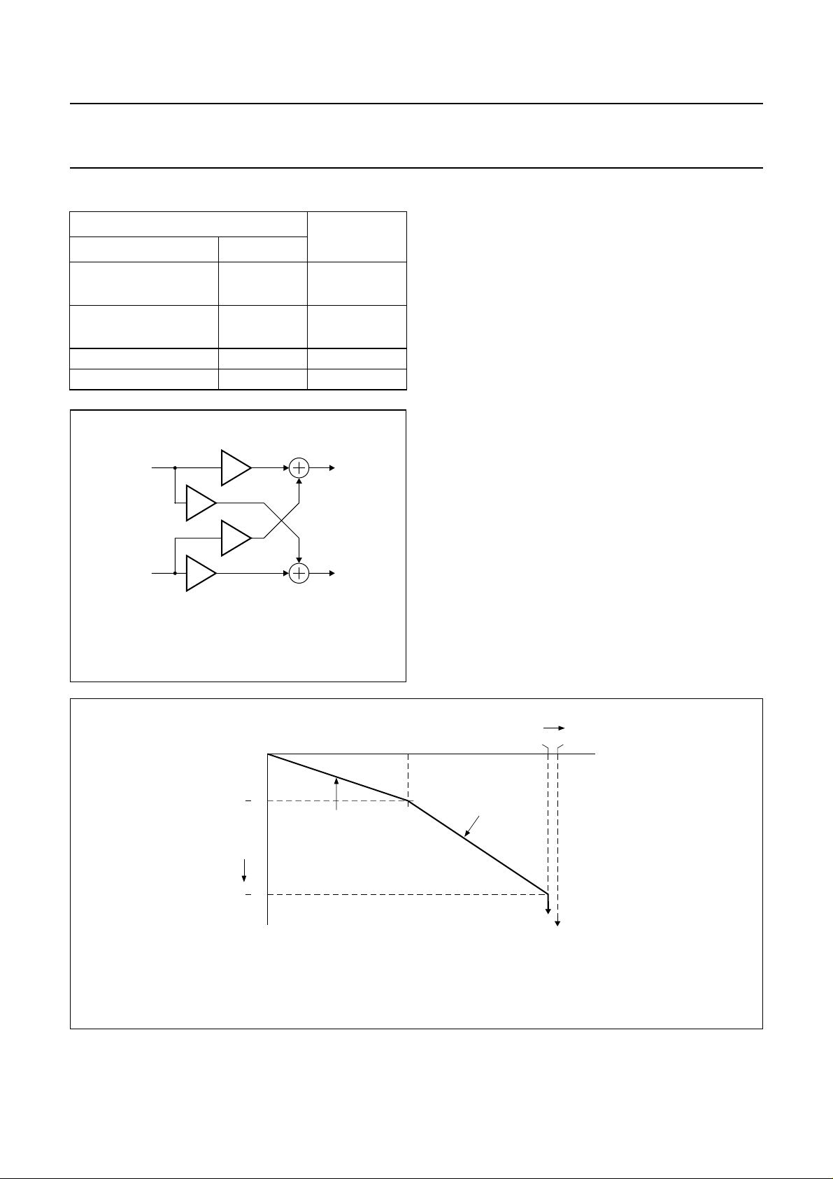
7.15 Baseband audio processing
The baseband audio de-emphasis as indicated in the
ISO/MPEG input data is performed digitally inside the
SAA2501. The incorporated ‘Audio Processing Unit’ (APU)
(see Fig.5) can be used to apply inter-channel crosstalk or
independent volume control per channel. The APU
attenuation coefficients LL, LR, RL and RR may be
changed dynamically by the host microcontroller, writing
their 8-bit indices to the SAA2501 over the L3 control bus.
The coefficient changes become effective within one
sample period after the coefficient index writing.
To avoid clicks at coefficient changes, the transition from
the current attenuation to the next is smoothed. The
relation between the APU coefficient index and the actual
coefficient (i.e. the gain) is given in Table 5.
January 1995 12
Philips Semiconductors Preliminary specification
Digital Audio Broadcast (DAB) decoder SAA2501
Table 5 APU coefficient index and actual coefficient
APU COEFFICIENT INDEX C
BINARY DECIMAL
00000000 to 00111111 0 to 63
01000000 to 01111110 64 to 126
APU
COEFFICIENT
C
–
-----12
2
C32–
–
---------------- 6
2
01111111 127 0
1XXXXXXX 128 to 255 reserved
left decoded
andbook, halfpage
audio
samples
right decoded
audio
samples
LL
LR
RL
RR
MGB493
left output
audio
samples
right output
audio
samples
From Table 5 we learned that up to coefficient index 64 the
step size is approximately −0.5 dB per coefficient
increment, and from coefficient index 64 to index 126 the
step size is approximately −1 dB per increment.
Note that the APU has no built-in overflow protection, so
the application must take care that the output signals of the
APU cannot exceed 0 dB level. For an update of the APU
coefficients, it may be required to increase some of the
coefficients and decrease some others. The APU
coefficients are always written sequentially in the fixed
sequence LL, LR, RL and RR. Therefore, to prevent
internal APU data overflow due to non-simultaneous
coefficient updating, the following steps can be followed:
1. Write LL, LR, RL, RR once, but change only those
coefficients that must decrease; overwrite the
coefficients that must increase with their old value (so
do not change these yet).
2. Write LL, LR, RL, RR again, but now change those
coefficients that must increase, keeping the other
coefficients unchanged.
The consequence of this two-pass coefficient updating is
that the application must keep a shadow of the current
APU coefficients (the L3 APU coefficients data item is
write-only).
Fig.5 Audio Processing Unit (APU).
handbook, full pagewidth
(1) Step −0.5 dB per coefficient increment.
(2) Step −1 dB per coefficient increment.
APU coefficient index
126 127
MGB494
gain
(dB)
0
0
32
(1)
94
64
(2)
Fig.6 Relation between APU coefficient index and gain.
January 1995 13
Philips Semiconductors Preliminary specification
Digital Audio Broadcast (DAB) decoder SAA2501
7.16 Decoding control signals
The decoding is performed by 3 signals as shown in
Table 6.
Table 6 Signals for decoding control
SIGNAL DIRECTION FUNCTION
RESET reset SAA2501 to
default state
STOP input stop decoding
URDA input unreliable input data;
interrupt decoding
The master reset signal RESET forces the SAA2501 into
its default state when HIGH. RESET must stay HIGH
during at least 24 MCLKIN periods if MCLKIN has
frequency of 24 MHz (i.e. MCLK24 = 1) or 12 MCLKIN
periods if MCLKIN has a frequency of 12 MHz
(MCLK24 = 0). At a reset, the SAA2501 synchronization to
the input bitstream is lost, the sub-band filter and
baseband audio output signals are muted, and the
SAA2501 settings are initialized.
The decoding can be stopped by making input signal
STOP HIGH. Stopping the decoding forces the SAA2501
to end decoding of input data, yet feeding zeroed
sub-band samples to the synthesis sub-band filter bank to
create a soft muting. When using the master input, input
requesting is also stopped. CDMWS stays in its current
state while STOP is asserted. The SAA2501 assumes the
input synchronization to be lost when the decoding is
stopped, thus causing re-synchronization when STOP is
(1)
de-activated again. Then the SAA2501 mutes, meanwhile
searching for a frame sync pattern or frame sync pulse (the
synchronization mode is selected via the L3 control bus) at
the input.
If synchronization is found, the SAA2501 starts producing
output data. The maximum response time to the activation
of signal STOP is half a sample period; the
re-synchronization time after STOP going LOW again
differs in various situations.
An ‘unreliable data’ indication can be given to the
SAA2501 by making signal URDA HIGH. URDA, like
STOP, mutes the sub-band signals and forces the
SAA2501 out of synchronization. However, in contrast to
STOP, master input data requesting continues at the bit
rate that was decoded before URDA became active. The
maximum response time to URDA is half a sample period.
7.17 Coded data interfaces
The SAA2501 contains:
• A coded data master input interface
• A coded data slave input interface (designed for EU147
format).
7.17.1 T
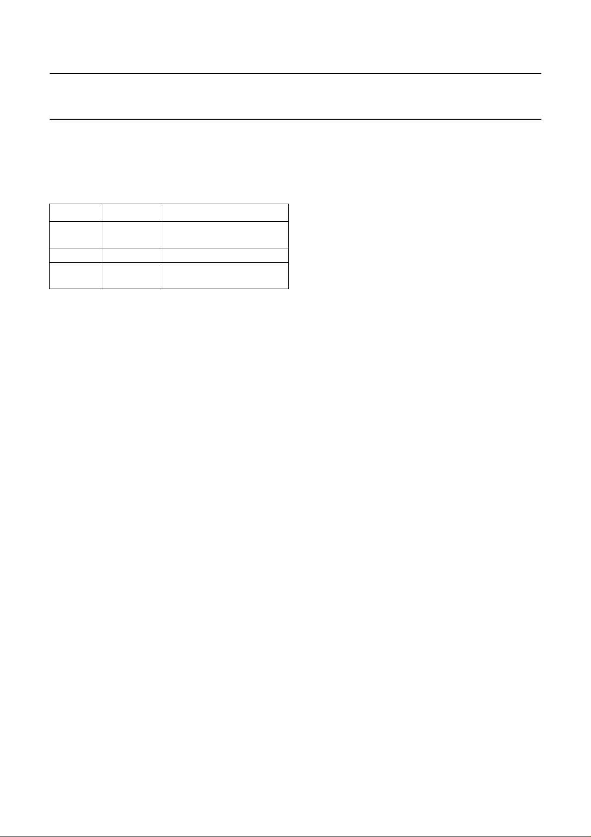
When using the master input, the SAA2501 requests for
input data. With the master input, the coded input data may
not use the ISO/MPEG free format bit rate or be in EU147
format. The coded data master input interface consists of
4 signals (see Fig.7).
HE CODED DATA MASTER INPUT INTERFACE
January 1995 14
Philips Semiconductors Preliminary specification
Digital Audio Broadcast (DAB) decoder SAA2501
Table 7 Signals of coded data master input interface
SIGNAL DIRECTION FUNCTION
CDM input ISO/MPEG coded input data (master input)
CDMEF input coded data (master input) error flag
CDMCL output coded data (master input) bit clock
CDMWS output coded data (master input) word select
handbook, full pagewidth
CDM
CDMCL
CDMWS
CDMEF
valid data valid but unreliable data invalid data
1 2 16 17 n 1 2
1 unreliable data bit (example)
Fig.7 Input data serial transfer format (master input).
Data clock CDMCL is being output, having a fixed
frequency of 768 kHz. Signal CDM carries the coded data
in bursts of 16 valid bits. Coded data input frames may
only start either at the first or at the ninth bit of a 16 bit valid
data burst (i.e. only at a byte boundary). The value of word
select signal CDMWS is changed every time new input
data is needed: one CDMCL period after each transition in
CDMWS, 16 bits of valid data are read serially. Assume N
is the number of CDMCL periods between two transitions
of CDMWS, and R is the number of CDMCL periods to
obtain the effective bit rate E (in kbits/s) at a transferring
data rate of 768 kbits/s, i.e. . The SAA2501R
16 768×
=
---------------------E
MGB495
keeps N close to R, but N can vary plus or minus two:
N ∈ {round(R)−2,...,round(R)+2}.
Error flag CDMEF is used to indicate input data
insecurities (e.g. due to erratic channel behaviour). In
Fig.7, an example with one unreliable bit is shown. The
value of CDMEF may vary for each valid data bit, but is
combined by the SAA2501 for every group of 8 input bits.
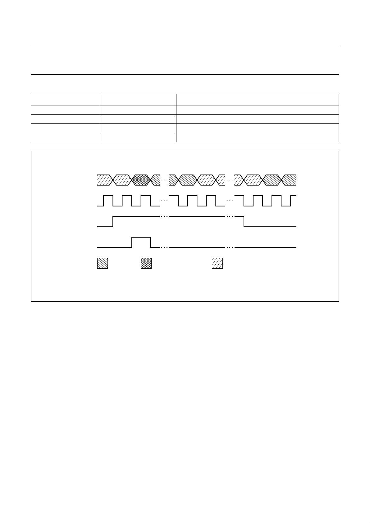
7.17.2 T
HE CODED DATA SLAVE INPUT INTERFACE
The coded data slave input interface signals are shown in
Fig.8. The coded data master input interface consists of
5 signals (see Table 8).
January 1995 15
Philips Semiconductors Preliminary specification
Digital Audio Broadcast (DAB) decoder SAA2501
Table 8 Signals of coded data slave input interface
SIGNAL DIRECTION FUNCTION
CDS input ISO/MPEG or EU147 coded input data (slave input)
CDSEF input coded data (slave input) error flag
CDSCL input coded data (slave input) bit clock
CDSWA input coded data (slave input) burst window signal
CDSSY input coded data (slave input) frame sync
handbook, full pagewidth
CDS
CDSCL
CDSWA
CDSSY
CDSEF
valid data valid but unreliable data invalid data
CDSSY indicates frame start during valid data.
frame start
Fig.8 Input data serial transfer format (slave input).
CDS is the SAA2501 input data bitstream. Data clock
CDSCL must have a frequency equal to or higher than the
bit rate. The maximum CDSCL frequency is 768 kHz. Error
flag CDSEF is handled in the same way as CDMEF is
handled for the master input (in Fig.8, one unreliable data
bit is shown as an example). The value of CDSEF is
neglected for those bits where CDSWA is LOW. Window
signal CDSWA being HIGH indicates valid data; in this
way, burst input data is allowed. The constraints for the
ability to use ‘burst signals’ are explained later in this
Section 7.17.2. Frame sync signal CDSSY indicates the
start of each input data frame. CDSSY is synchronous with
CDSCL. CDSSY may be present or not: as described later
1 unreliable data bit (example)
MGB496
in this Section 7.17.2. The first valid CDS bit after a leading
edge of CDSSY is interpreted to be the first frame bit.
The minimum time for CDSSY to stay HIGH is one CDSCL
period; the maximum HIGH period is constrained by the
requirement that CDSSY must be LOW at least during one
CDSCL period per frame (a leading edge, i.e. a frame start
indication, must be present every frame). Leading edges
of CDSSY can occur while CDSWA is HIGH, as in Fig.8.
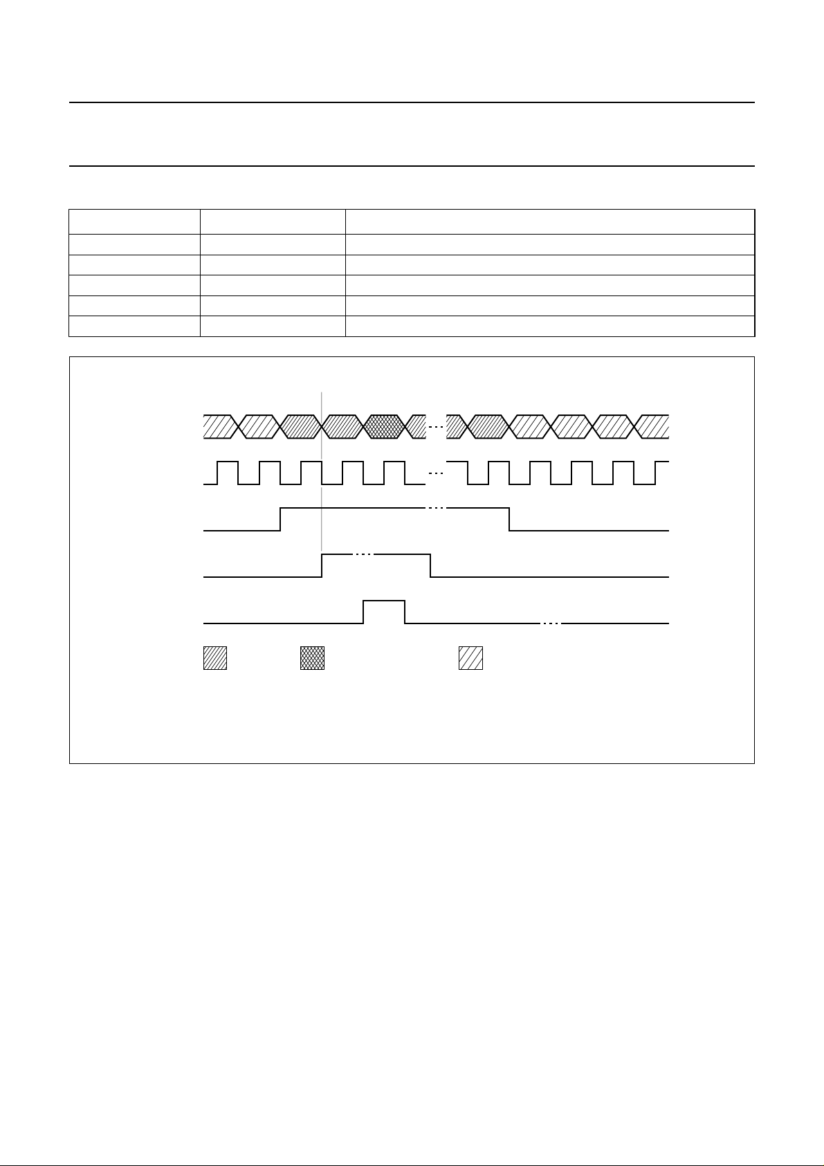
Alternatively, a situation as shown in Fig.9 is also allowed,
where CDSSY has a leading edge while CDSWA is LOW,
i.e. during invalid data. The first CDS bit after CDSWA
going HIGH is now interpreted to be the first frame bit.
January 1995 16
 Loading...