

Philips saa2032 DATASHEETS
INTEGRATED CIRCUITS
DATA SH EET
SAA2032
Digital equalization for the tape
drive processing of the DCC system
Product specification
Supersedes data of February 1993
File under Integrated Circuits, Miscellaneous
Philips Semiconductors
February 1995
Philips Semiconductors Product specification
Digital equalization for the tape
SAA2032
drive processing of the DCC system
FEATURES
• Analog-to-digital conversion, demultiplexing,
equalization and zero crossing of time multiplexed
analog read amplifier signal
• Microcontroller interface
• Search mode envelope, label and virgin detection of the
AUX channel
• Search mode tape speed measurement
• Simplified external biassing
• Reduced power consumption
• Analog eye output
• 4 V nominal operating voltage capability.
ORDERING INFORMATION
GENERAL DESCRIPTION
Performing the Digital Equalizing function in the Digital
Compact Cassette (DCC) system, the SAA2032 is
intended for use in conjunction with the SAA2022, read
amplifier TDA1317 or TDA1318.
EXTENDED TYPE
NUMBER
SAA2032GP
Note
1. When using reflow soldering it is recommended that the Dry Packing instructions in the
are followed. The pocketbook can be ordered using the code 9398 510 34011.
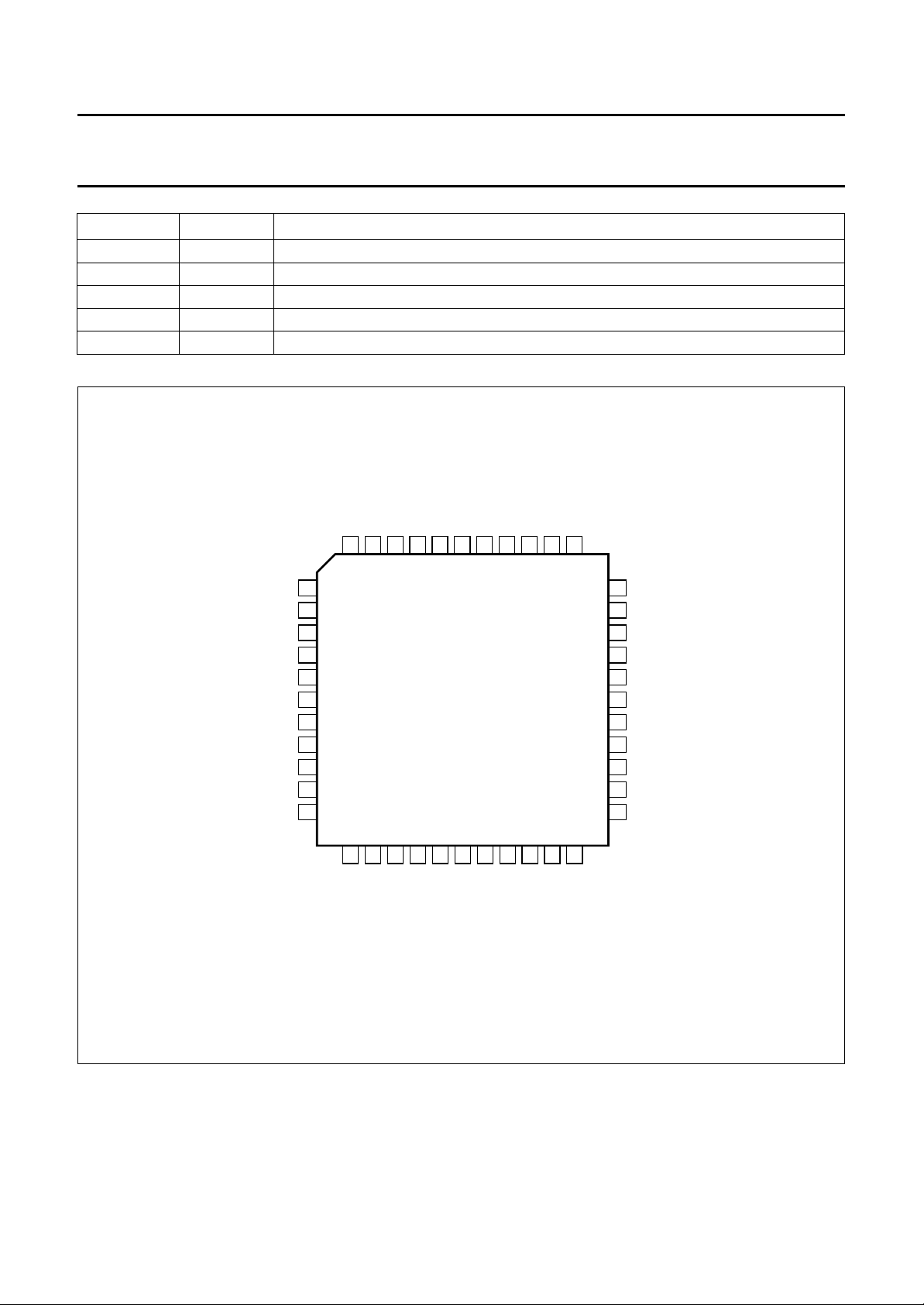
PINS PIN POSITION MATERIAL CODE
44 QFP 1 plastic SOT205AG
PACKAGE
Quality Reference Pocketbook
February 1995 2
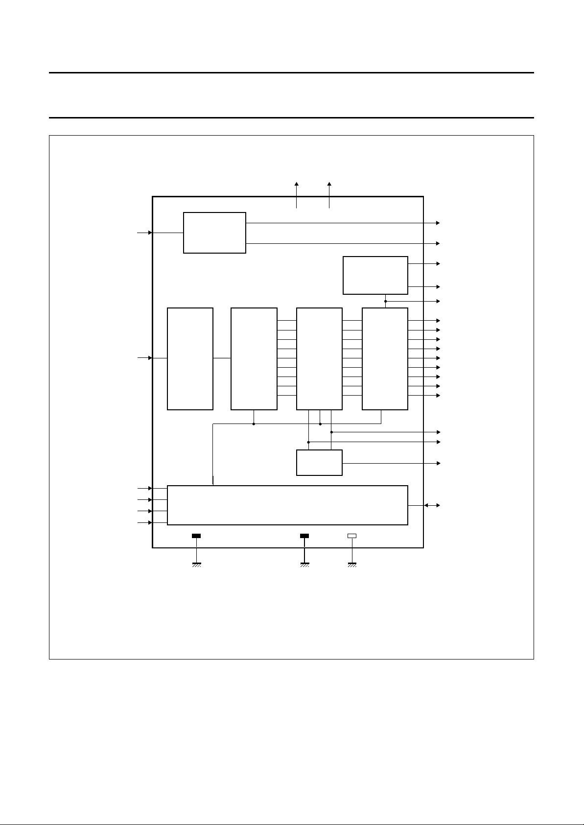
Philips Semiconductors Product specification
Digital equalization for the tape
drive processing of the DCC system
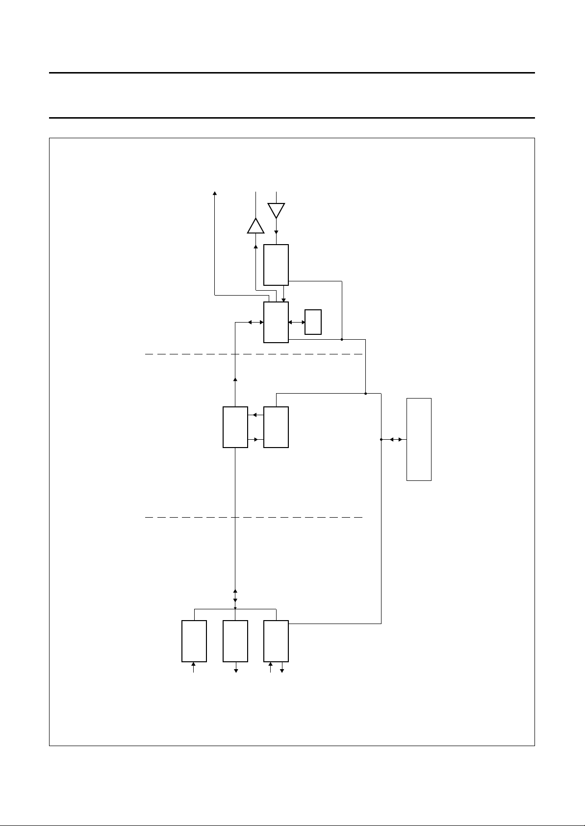
24f
VIN
43
5
CLOCK
GENERATION
V
DDAD
11 12
SAA2032
SAA2032
V
DD
3
RDCLK
2
RDSYNC
VIRGIN
LABEL
DETECTOR
SLICERFILTERDEMUXADC
37
36
38
22
23
24
25
26
27
28
29
30
LABEL
VIRGIN
AENV
CH0
CH1
CH2
CH3
CH4
CH5
CH6
CH7
AUX
LTENDEQ
LTCNT1
LTCNT0
LTCLK
1
44
DAC ANEYE
32
33
34
35
8, 14
V
SSA
LT
INTERFACE
V
SSAD
10
13, 17, 39
V
SS
15
31
MEA663
DIGEYE
VAL
LTDATA
Fig.1 Block diagram.
February 1995 3
Philips Semiconductors Product specification
Digital equalization for the tape
SAA2032
drive processing of the DCC system
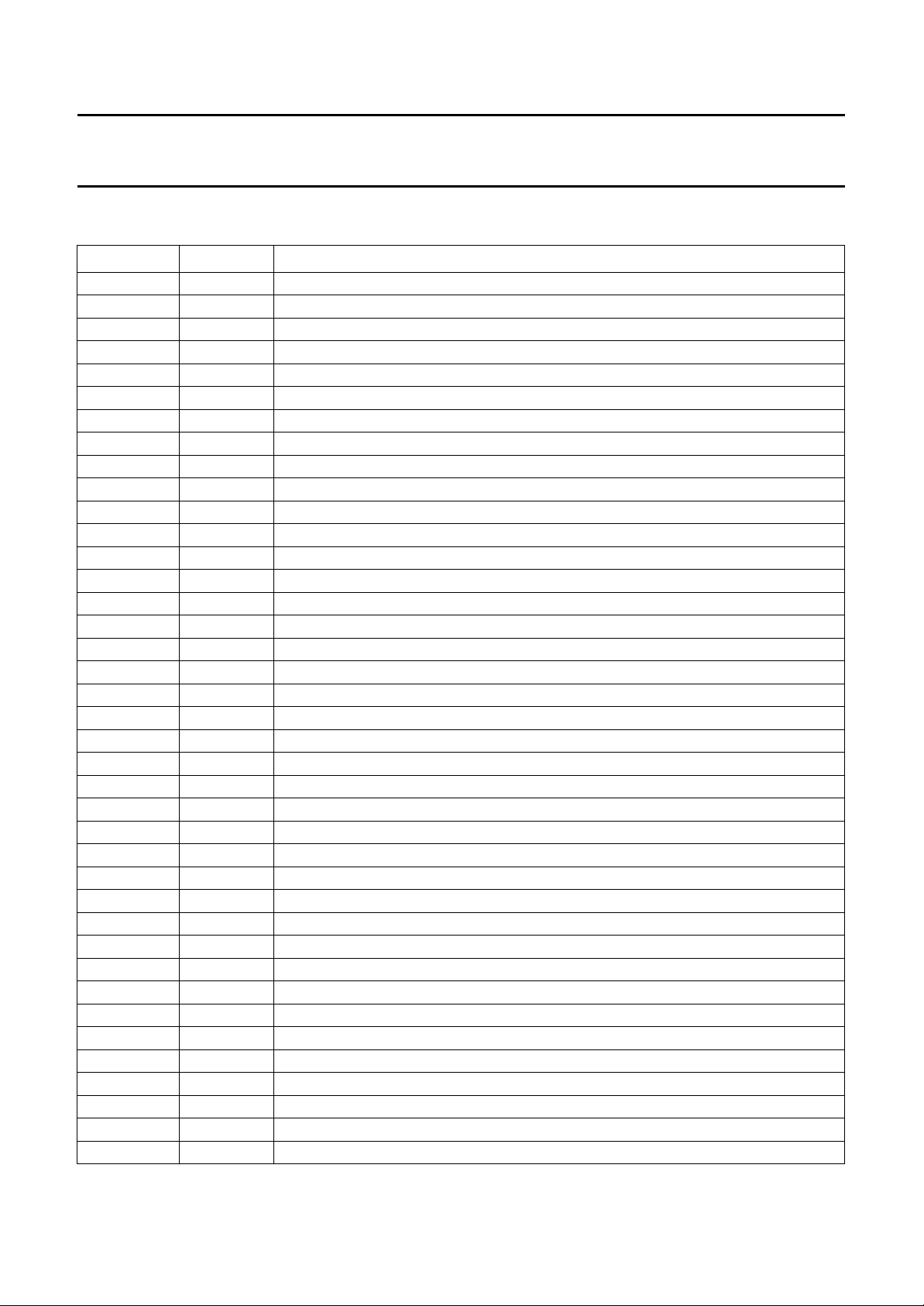
PINNING
SYMBOL PIN DESCRIPTION
DIGEYE 1 serial data output for eye pattern
RDSYNC 2 SYNC data for Read Amplifier (push-pull output)
RDCLK 3 data clock for Read Amplifier (push-pull output)
TEST1 4 test 1; to be connected to V
VIN 5 analog time multiplexed input from Read Amplifier
REFN 6 lower reference voltage (+1 V) for ADC
REFP 7 upper reference voltage (+3.1 V) for ADC
V
SSA
8 analog ground (0 V)
BIASA 9 bias current for ADC (sinks current from V
V
V
V
V
V
SSAD
DDAD
DD
SS
SSA
10 supply ground (0 V) for ADC
11 supply voltage (+5 V) for ADC
12 supply voltage (+5 V)
13 supply ground (0 V)
14 supply ground (0 V)
ANEYE 15 analog eye voltage output
n.c. 16 not connected
V
SS
17 supply ground (0 V)
TEST4 18 test 4; do not connect
TEST5 19 test 5; do not connect
TEST6 20 test 6; do not connect
TEST7 21 test 7; do not connect
CH0 22 channel 0 output for SAA2022 (DCC Drive Signal Processing) (push-pull output)
CH1 23 channel 1 output for SAA2022 (push-pull output)
CH2 24 channel 2 output for SAA2022 (push-pull output)
CH3 25 channel 3 output for SAA2022 (push-pull output)
CH4 26 channel 4 output for SAA2022 (push-pull output)
CH5 27 channel 5 output for SAA2022 (push-pull output)
CH6 28 channel 6 output for SAA2022 (push-pull output)
CH7 29 channel 7 output for SAA2022 (push-pull output)
AUX 30 AUX channel output for SAA2022 (push-pull output)
LTDATA 31 microcontroller I/O data interface (3-state push-pull output and input; CMOS levels)
LTENDEQ 32 microcontroller interface enabling (CMOS input levels)
LTCNT1 33 microcontroller interface; mode control 1 (CMOS input levels)
LTCNT0 34 microcontroller interface; mode control 0 (CMOS input levels)
LTCLK 35 microcontroller bit-clock interface (CMOS input levels)
VIRGIN 36 search mode virgin detection output
LABEL 37 search mode label detection output
AENV 38 search mode auxiliary detection output
V
SS
39 supply ground (0 V)
SS
via 33 kΩ)
DDAD
February 1995 4
Philips Semiconductors Product specification
Digital equalization for the tape
drive processing of the DCC system
SYMBOL PIN DESCRIPTION
TEST8 40 test 8 input; to be connected to V
TEST9 41 test 9 input; to be connected to V
TEST10 42 test 10 input; to be connected to V
f24 43 clock input; typical frequency 24.576 MHz (CMOS input)
VAL 44 synchronization output for DIGEYE
f24
TEST10
DIGEYE
RDSYNC
RDCLK
TEST1
VIN
REFN
REFP
V
SSA
BIASA
V
SSAD
V
DDAD
VAL
44
43
1
2
3
4
5
6
7
8
9
10
11
42
TEST9
TEST8
41
40
SAA2032
SS
SS
SS
SS
AENV
V
39
38
LABEL
37
LTCLK
VIRGIN
36
35
LTCNT0
34
33
32
31
30
29
28
27
26
25
24
23
SAA2032
LTCNT1
LTENDEQ
LTDATA
AUX
CH7
CH6
CH5
CH4
CH3
CH2
CH1
15
14
SSA
V
16
n.c.
ANEYE
12
13
SS
DD
V
V
Fig.2 Pin configuration.
February 1995 5
18
20
22
19
TEST5
21
TEST7
TEST6
MEA661
CH0
17
SS
V
TEST4
Philips Semiconductors Product specification
Digital equalization for the tape
drive processing of the DCC system
write
and
heads
drive
capstan
TDA1319
TDA1316 or
speed control
tape
SAA2032
SAA2022
read
TDA1317 or
digital
equalizer
TDA1318
RAM
256 kbits
SAA2032
TAPE DRIVE PROCESSING
MEA695 - 2
ADC
SAA7360
codec
stereo filter
2
I S
DAC
2
I S
(sub-band)
SAA2002
SAA7323
SAA2012
DAIO
TDA1315
adaptive
scale factors
allocation and
MICROCONTROLLER
Fig.3 DCC data flow diagram.
RECORDING + PLAY BACK
input
analog
output
analog
digital input
digital output
February 1995 6
AUDIO INPUT/OUTPUT PASC PROCESSING
Philips Semiconductors Product specification
Digital equalization for the tape
SAA2032
drive processing of the DCC system
FUNCTIONAL DESCRIPTION
Operating Modes
DEQ operating modes are programmed via the LT
interface:
ORMAL
N
• A/D conversion
• Demultiplexing
• Equalization
• Zero crossing.
in this mode the SAA2032 performs the equalization and
slicing of the eight data channels and the auxiliary channel.
The eight data channels have a bit-rate of 96 kbits/s while
the auxiliary channel has a bit-rate of 12 kbits/s.
The SAA2032 input is a time-multiplexed analog signal
from the Read Amplifier. The signal contains ten time slots,
of which nine are used. The Read Amplifier and the
SAA2032 synchronize with the RDCLK and RDSYNC
signals generated by the SAA2032.
Following A/D conversion and demultiplexing the nine
channels are equalized. The encoding of the equalizing
coefficients (12 per channel) are not fixed and must be
loaded via the LT interface before operation.
The nine equalized output signals are up-sampled by a
factor of 10 with the resulting signals fed to the slicer. The
slicer output is applied to the SAA2022.
EST
T
• A/D conversion
• Demultiplexing
• Equalization
• Zero crossing
• Eye-pattern.
Same as normal mode. In addition the digital and analog
eye-pattern outputs are enabled. The eye-pattern output
corresponds to one of the equalized channel outputs.
EARCH
S
• A/D conversion
• Envelope detection
• Tape search and speed measurement.
In the search mode the analog input signal from the Read
Amplifier is not the multiplexed signal but only the auxiliary
channel signal.
Following A/D conversion the envelope of this signal is
filtered and sliced. This forms the Alternating Envelope
AENV output. The LABEL and VIRGIN outputs are
detected from this and the tape search speed measured.
FF
O
In the OFF mode the RDSYNC and RDCLK signals are
HIGH, the EYE outputs are disabled and the channel and
auxiliary outputs (CH0 to CH7 and AUX) are 3-stated.
Read Amplifier interface
The interface between the Read Amplifier and the
SAA2032 consists of three signals:
1. VIN from Read Amplifier to SAA2032; time
multiplexed data.
2. RDSYNC from SAA2032 to Read Amplifier;
synchronization between Read Amplifier multiplexer
and SAA2032 demultiplexer.
3. RDCLK from SAA2032 to Read Amplifier; data clock
for Read Amplifier multiplexer.
The multiplexed VIN output of the Read Amplifier changes
to another channel at the rising edge of RDCLK. RDSYNC
synchronizes the Read Amplifier VIN output: if RDSYNC is
HIGH, the rising edge of the RDCLK will select the AUX
channel.
Figures 4 and 5 show the relationship between the
SAA2032 and the Read Amplifier.
SAA2022 interface
The interface with the SAA2022 consists of the 9 data
output signals CH0 to CH7, AUX.
Table 1 Dependency of Read Amplifier on
operational mode.
OPERATIONAL MODE RDSYNC RDCLK
Normal YES YES
Test YES YES
Search HIGH YES
Off HIGH HIGH
Label and virgin detection interface
When the DCC player is in its search mode, the tape is
fast-wound while the head retains tape contact. The
SAA2032 can be made to operate in the search mode and
the information will be read from the auxiliary tape track.
February 1995 7
Philips Semiconductors Product specification
Digital equalization for the tape
SAA2032
drive processing of the DCC system
The following three signals are generated:
1. LABEL: label detection (HIGH if label is detected).
2. VIRGIN: virgin tape detection (HIGH if virgin tape
is detected).
3. AENV: alternating envelope (sliced envelope).
AENV, LABEL and VIRGIN are disabled in normal or off
modes. LABEL, VIRGIN and AENV are LOW.
AENV, LABEL and VIRGIN are enabled when the
SAA2032 is in search mode.
The device detects the envelope AENV of the auxiliary
track at search speeds between 3 and 50 times normal
speed. If AENV is continuously HIGH (label detection),
LABEL will be HIGH.
When AENV is continuously LOW (virgin tape detection)
VIRGIN will be HIGH.
Figures 6, 7 and 8 show the relationship between AENV,
VIRGIN and LABEL.
Labelled tape-speed calculation
When the DCC player is in its search mode, the tape
speed increases. LABEL information is encoded
throughout its length. To examine the length of a label, the
tape speed must be known. In search mode the SAA2032
assesses the speed of labelled tapes. The microcontroller
obtains this information via the LT-interface.
The speed information is encoded in 3 variables:
1. SVF Speed Validation Flag (HIGH if invalid).
2. SC (4..0) Speed counter.
3. SR (1..0) Speed Range.
51.2
SR
-----------
Search speed 2
×= x normal speed.
SC
If SC = 0 then search speed > 51.2.
With SR = 0, 1, 2 or 3 and SC = 0 to 31.
If SVF = 1 then SR and SC values are invalid.
Appendix 1 gives a table of the search mode speed
control.
Microcontroller (LT) Interface
The SAA2032 is able to exchange information with the
microcontroller via the LT-interface. The microcontroller
performs as master, the SAA2032 as slave.
Figure 9 gives the operation of the LT-interface.
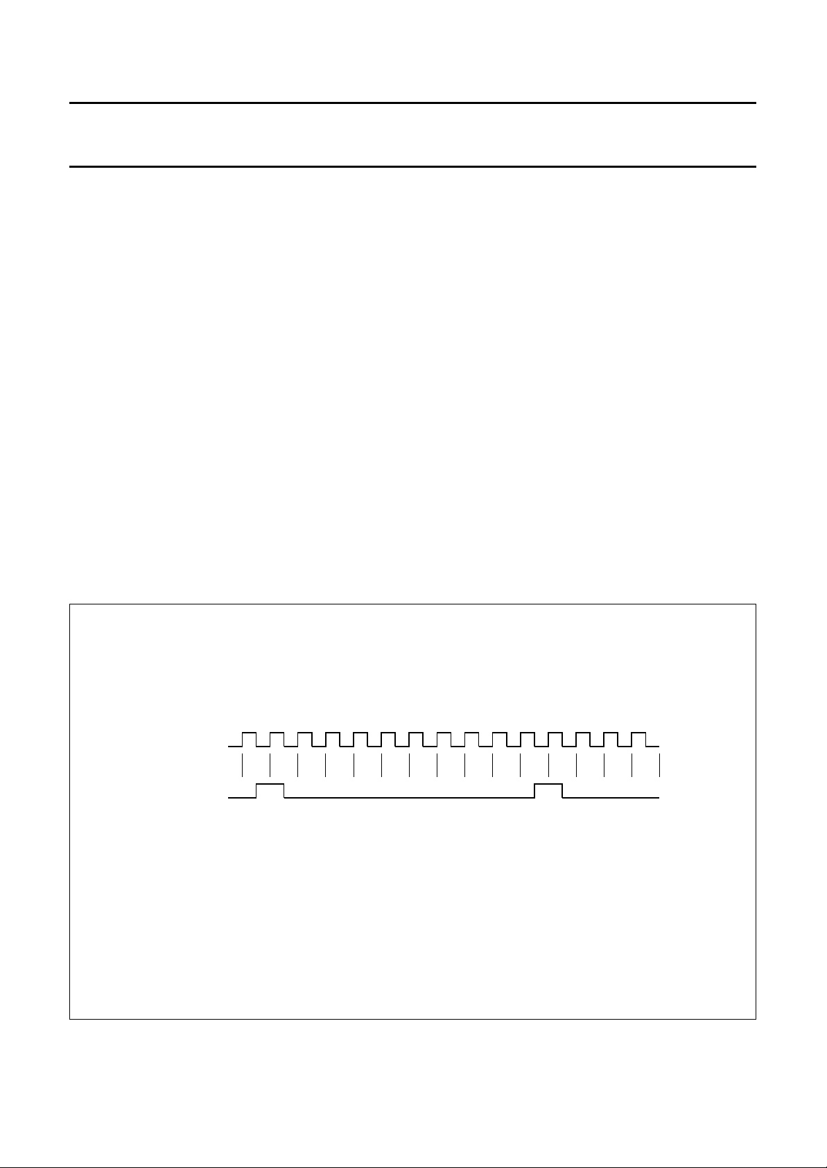
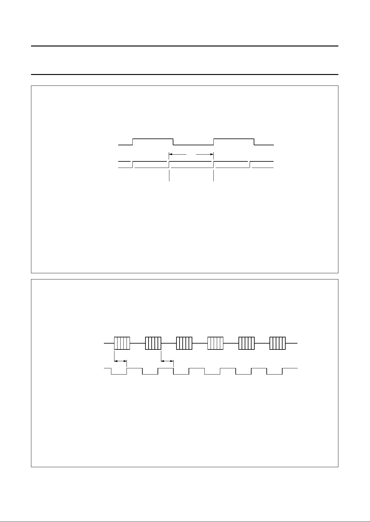
RDCLK
VIN
RDSYNC
CH7 AUX
CH0 CH3 CH4 CH5 CH6 CH7 AUX
***
Fig.4 Signals on interface between Read Amplifier and SAA2032.
February 1995 8
***
CH0CH2CH1 CH1
MCD477
Philips Semiconductors Product specification
Digital equalization for the tape
SAA2032
drive processing of the DCC system
RDCLK
t
su
VIN
VIN
stable
MCD478
tsu > 80 ns; set-up time VIN before RDCLOCK HIGH.
Typical frequency for RDCLK = 3.072 MHz.
Typical frequency for RDSYNC = 307.2 kHz.
Fig.5 Timing.
signal
from
tape
t
d2
AENV
t
d1
MCD488 - 1
td1 = td2 = between 0.5 and 1.0 auxiliary block lengths.
Fig.6 Diagram of AENV signal.
February 1995 9
 Loading...