

Philips saa2022 DATASHEETS

INTEGRATED CIRCUITS
DATA SH EET
SAA2022
Tape formatting and error
correction for the DCC system
Product specification
Supersedes data of February 1993
File under Integrated Circuits, Miscellaneous
Philips Semiconductors
February 1994
Philips Semiconductors Product specification
Tape formatting and error
correction for the DCC system
FEATURES
• Integrated error correction encoder/decoder function
with Digital Compact Cassette (DCC) optimized
algorithms
• Control of capstan servo during recording and after
recording by microcontroller
• Frequency and phase regulation of capstan servo
during playback
• Choice of two Dynamic Random Access Memory
(DRAM) types operating in page mode
• Scratch pad RAM area available to microcontroller in
system DRAM
• Low power standby mode
• I2S interface
• Microcontroller interface for high-speed transfer burst
rates up to 170 kbytes per second
• SYSINFO and AUXILIARY data flags on microcontroller
interface
• Protection against invalid AUXILIARY data
• +4 V operating voltage capability.
SAA2022
GENERAL DESCRIPTION
Performing the tape formatting and error correction
functions for DCC applications, the SAA2022 can be used
in conjunction with the PASC (SAA2002/SAA2012), tape
equalization (SAA2032), read amplifier (TDA1317 or
TDA1318) and write amplifier (TDA1316 or TDA1319)
circuits to implement a full signal processing system.
ORDERING INFORMATION
EXTENDED TYPE
NUMBER
SAA2022GP 64 QFP
Note
1. When using reflow soldering it is recommended that the Dry Packing instructions in the
Pocketbook”
are followed. The pocketbook can be ordered using the code 9398 510 34011.
PINS PIN POSITION MATERIAL CODE
(1)
PACKAGE
plastic SOT208A
“Quality Reference
February 1994 2

February 1994 3
V
DD1VDD2VDD3VDD4
LTCLK
LTEN
LTCNT1
LTCNT0
PINI
SBEF
SBDA
SBCL
SBWS
SBMCLK
TCH0 - 7,
TAUX
RESET
PWRDWN
CLK24
5
6
3
4
49
57
62
61
60
56
33–41
48
47
44
TAPE INPUT
BUFFER
TAPE OUTPUT
BUFFER
CLOCK
GENERATOR
SAA2022
2
SB – I S
INTERFACE
CONTROL
MICROCONTROLLER
INTERFACE
43 8 27 59
ERROR
CORRECTION
CODER
DRAM
INTERFACE
26742
V
SS1VSS2VSS3VSS4
58
17–25
11–14
29
28
32
50
51
15
10
16
64
63
30
31
52
55
2
9
1
LTDATA
WDATA
WCLOCK
PINO1
PINO2
PINO3
RASN
CASN
A0–8
D0–3
WEN
OEN
LTREF
URDA
SBDIR
SPEED
SPDF
AZCHK
MCLK
MEA711 - 2
BLOCK DIAGRAM
correction for the DCC system
SAA2022
Philips Semiconductors Product specification
Tape formatting and error
Fig.1 Block diagram.

Philips Semiconductors Product specification
Tape formatting and error
correction for the DCC system
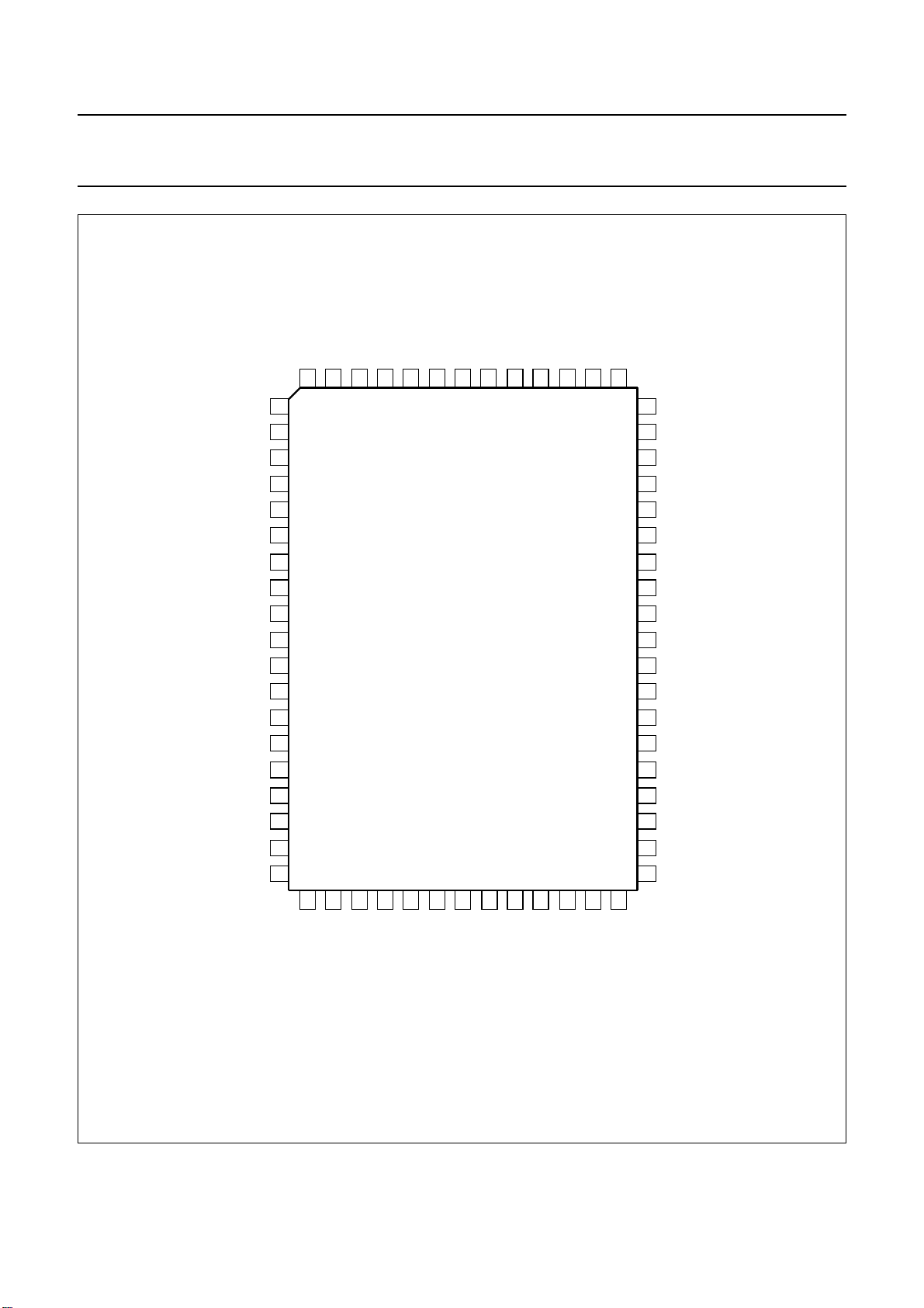
PINNING
SYMBOL PIN DESCRIPTION
LTREF 1 timing reference for microcontroller interface
LTDATA 2 data for microcontroller interface (3-state; CMOS levels)
LTCNT1 3 control for microcontroller interface
LTCNT0 4 control for microcontroller interface
LTCLK 5 bit clock for microcontroller interface
LTEN 6 enable for microcontroller interface
V
SS2
V
DD2
RASN 9 DRAM row address strobe
WEN 10 DRAM write enable
D3 11 DRAM data (MSB); 3-state output; TTL compatible input
D2 12 DRAM data; 3-state output; TTL compatible input
D1 13 DRAM data; 3-state output; TTL compatible input
D0 14 DRAM data (LSB); 3-state output; TTL compatible input
CASN 15 DRAM column address strobe
OEN 16 DRAM output enable
A8 17 DRAM address (MSB)
A7 18 DRAM address
A6 19 DRAM address
A5 20 DRAM address
A4 21 DRAM address
A3 22 DRAM address
A2 23 DRAM address
A1 24 DRAM address
A0 25 DRAM address (LSB)
V
SS3
V
DD3
WCLOCK 28 clock for write amplifier transfers
WDATA 29 write amplifier serial data
SPEED 30 capstan phase information
SPDF 31 capstan frequency information
PINO1 32 Port expander output 1
TAUX 33 AUX channel input from SAA2032
TCH7 34 main data channel 7, input from SAA2032
TCH6 35 main data channel 6, input from SAA2032
TCH5 36 main data channel 5, input from SAA2032
TCH4 37 main data channel 4, input from SAA2032
TCH3 38 main data channel 3, input from SAA2032
TCH2 39 main data channel 2, input from SAA2032
7 supply ground (0 V)
8 supply voltage (+5 V)
26 supply ground (0 V)
27 supply voltage (+5 V)
SAA2022
February 1994 4
Philips Semiconductors Product specification
Tape formatting and error
correction for the DCC system
SYMBOL PIN DESCRIPTION
TCH1 40 main data channel 1, input from SAA2032
TCH0 41 main data channel 0, input from SAA2032
V
SS1
V
DD1
CLK24 44 24.576 MHz clock from SAA2002
TEST0 45 test select LSB; do not connect
TEST1 46 test select MSB; do not connect
PWRDWN 47 sleep mode selection
RESET 48 reset input with hysteresis and pull-down resistor
PINI 49 Port expander input
PINO2 50 Port expander output 2
PINO3 51 Port expander output 3
AZCHK 52 azimuth check (channels 0 and 7)
TEST2 53 symbol error rate measurement output
TEST3 54 do not connect
MCLK 55 master clock output (6.144 MHz)
SBMCLK 56 master clock for SB-I
SBEF 57 byte error SB-I
V
SS4
V
DD4
SBWS 60 word select SB-I
SBCL 61 bit clock SB-I
SBDA 62 data line SB-I
SBDIR 63 direction SB-I
URDA 64 unusable data SB-I
42 supply ground (0 V)
43 supply voltage (+5 V)
2
S-interface
58 supply ground (0 V)
59 supply voltage (+5 V)
2
S-interface; 3-state output; CMOS levels
2
S-interface; 3-state output; CMOS levels
2
S-interface; 3-state output; CMOS levels
2
S-interface
2
2
S-interface
S-interface
SAA2022
February 1994 5
Philips Semiconductors Product specification
Tape formatting and error
correction for the DCC system
SBDIR
SBDA
63
62
LTREF
LTDATA
LTCNT1
LTCNT0
LTCLK
LTEN
V
SS2
V
DD2
RASN
WEN
D3
D2
D1
D0
URDA
64
1
2
3
4
5
6
7
8
9
10
11
12
13
14
SBCL
61
V
SBWS
60
SAA2022
DD4
59
V
58
SS4
SBEF
57
MCLK
SBMCLK
56
55
TEST3
54
TEST2
53
AZCHK
52
51
50
49
48
47
46
45
44
43
42
41
40
39
38
PINO3
PINO2
PINI
RESET
PWRDWN
TEST1
TEST0
CLK24
V
DD1
V
SS1
TCH0
TCH1
TCH2
TCH3
SAA2022
CASN
15
OEN
16
17
A8
A7
18
A6
19
20
21
A5
A4
22
A3
23
A2
24
A1
25
A0
Fig.2 Pin configuration (SOT208A).
February 1994 6
26
V
SS3
27
DD3
V
28
29
WDATA
WCLOCK
30
SPEED
31
SPDF
37
36
35
34
33
32
PINO1
TCH4
TCH5
TCH6
TCH7
TAUX
MEA693 - 2

February 1994 7
FUNCTIONAL DESCRIPTION
correction for the DCC system
Philips Semiconductors Product specification
Tape formatting and error
RECORDING + PLAY BACK
analog
input
analog
output
digital input
digital output
ADC
SAA7360
DAC
SAA7323
DAIO
TDA1315
2
I S
stereo filter
codec
SAA2002
SAA2012
adaptive
allocation and
scale factors
AUDIO INPUT/OUTPUT PASC PROCESSING
MICROCONTROLLER
2
I S
(sub-band)
MEA695 - 2
speed control
TDA1316 or
TDA1319
SAA2022
RAM
256 kbits
SAA2032
digital
equalizer
TAPE DRIVE PROCESSING
write
read
TDA1317 or
TDA1318
capstan
drive
heads
and
tape
Fig.3 DCC data flow diagram.
SAA2022

Philips Semiconductors Product specification
Tape formatting and error
correction for the DCC system
The SAA2022 provides the following functions:
In Playback Modes
• Tape channel data and clock recovery
• 10 to 8 demodulation
• Data placement in DRAM
• C1 and C2 error correction decoding
2
S-interfacing to SB-I2S-bus
• I
• Interfacing to microcontroller for SYSINFO and
AUX data
• Capstan control for tape deck.
In Record Modes
2
S-interfacing to SB-I2S-bus
• I
• C1 and C2 error correction encoding
• Formatting for tape transfer
• 8 to 10 modulation
• Interfacing to microcontroller for SYSINFO and
AUX data
• Capstan control for tape deck, programmable by
microcontroller.
SAA2022
PWRDWN
This pin is an active HIGH signal which places the
SAA2022 in a “SLEEP” mode. When the SAA2022 is in
“SLEEP” mode and the CLK24 is either held HIGH or held
LOW, there is no activity in the device, thus resulting in
no EMI and a low power dissipation (typically <10% of
operational dissipation). This pin should be connected to
the DCC power-down signal, which can be driven by the
system microcontroller.
To enter the “SLEEP” mode the SAA2022 should reset
and hold reset. After a delay of at least 15 µs the
PWRDWN pin should be brought HIGH after which the
state of the reset pin is “don’t care”. The power dissipation
is reduced further when the CLK24 input signal stops.
When recovering from “SLEEP” mode the PWRDWN pin
should be driven LOW and the chip reset with a pulse of at
least 15 µs duration.
CLK24
This is the 24.576 MHz clock input and should be
connected directly to the SAA2002 CLK24 pin.
Connections to SAA2032
TCH0
TO TCH7 AND TAUX
Operational Modes
The 3 basic modes of operation are:
• DPAP - Main data (audio) and SYSINFO play, AUX play
• DRAR - Main data (audio) and SYSINFO record,
AUX record
• DPAR - Main data (audio) and SYSINFO play,
AUX record.
Hardware Interfacing
RESET
This is an active HIGH input signal which resets the
SAA2022 and brings it into its default mode, DPAP. This
should be connected to the system reset, which can be
driven by the microcontroller. The duration of the reset
pulse should be at least 15 µs. This pin has an internal
pull-down resistor of between 20 kΩ and 125 kΩ.
These lines are the equalized and clipped (to VDD) tape
channel inputs and should be connected to the SAA2032
pins TCH0 to TCH7 and TAUX.
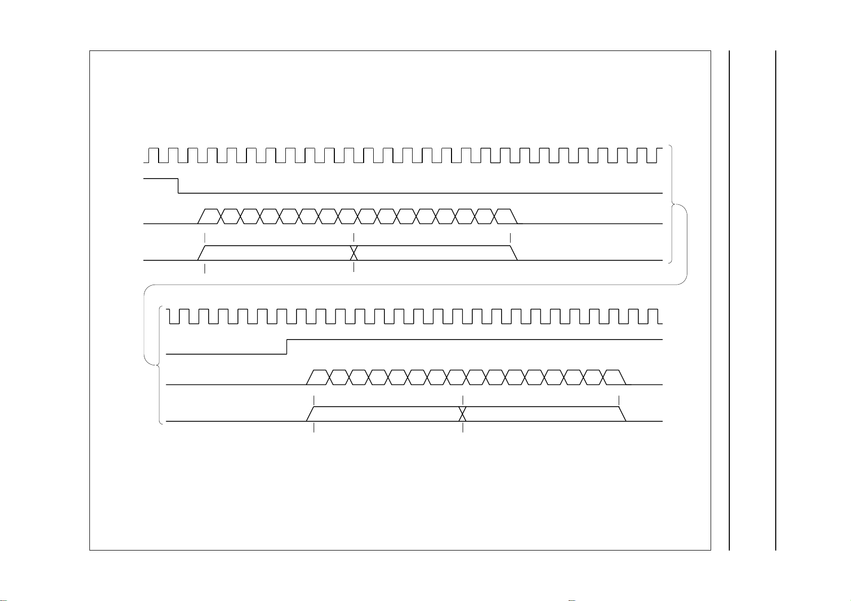
Sub-band I
The timing for the SB-I2S-interface is given in Figs 4 to 9.
2
S-bus Connections
February 1994 8

February 1994 9
lines show rising edge of SBMCLK
SBMCLK
SBCL
SBWS
SBDA
bit number
byte number
SBEF
0 1 2 3 4 5 6 7 8 9 10 11 12 13 14 15
01
01byte number
correction for the DCC system
Philips Semiconductors Product specification
Tape formatting and error
16 17 18 19 20 21 22 23 24 25 26 27 28 29 30 31
23
23
Fig.4 SB-I2S-interface in playback master mode (1).
MEA697 - 1
SAA2022

February 1994 10
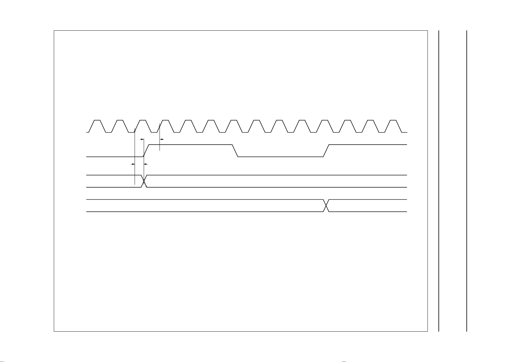
SBMCLK
(INPUT)
SBCL
(OUTPUT)
SBWS
(OUTPUT)
SBEF
(OUTPUT)
MCLK
(OUTPUT)
SBDA
(OUTPUT)
Philips Semiconductors Product specification
Tape formatting and error
correction for the DCC system
t
H-1
t
L-1
t
dSR
t
suMR
t
dSR
t
suMR
t
dMR
SBEF
(OUTPUT)
MEA696
SAA2022
Fig.5 SB-I2S-interface in playback master mode (2).
February 1994 11
SBCL
SBWS
SBDA
bit number
byte number
SBEF
0 1 2 3 4 5 6 7 8 9 10 11 12 13 14 15
01
Philips Semiconductors Product specification
Tape formatting and error
correction for the DCC system
16 17 18 19 20 21 22 23 24 25 26 27 28 29 30 31
23
Fig.6 SB-I2S-interface in playback slave mode (1).
MEA699 - 1
SAA2022

February 1994 12
MCLK
SBCL
(INPUT)
SBWS
(INPUT)
SBEF
(OUTPUT)
t
hMR
t
suMR
t
hMR
t
suMR
Philips Semiconductors Product specification
Tape formatting and error
correction for the DCC system
SBDA
(OUTPUT)
Fig.7 SB-I2S-interface in playback slave mode (2).
t
dMR
MEA698
SAA2022
February 1994 13
SBCL
SBWS
SBDA
bit number
byte number
0 1 2 3 4 5 6 7 8 9 10 11 12 13 14 15
01
Philips Semiconductors Product specification
Tape formatting and error
correction for the DCC system
16 17 18 19 20 21 22 23 24 25 26 27 28 29 30 31
23
Fig.8 SB-I2S-interface in record mode (1).
MSA536
SAA2022
February 1994 14
MCLK
(OUTPUT)
SBCL
(INPUT)
SBWS
(INPUT)
SBDA
(INPUT)
t
hMR
t
suMR
MEA700
Philips Semiconductors Product specification
Tape formatting and error
correction for the DCC system
Fig.9 SB-I2S-interface in record mode (2).
SAA2022

Philips Semiconductors Product specification
Tape formatting and error
correction for the DCC system
SBMCLK
This is the sub-band master clock input for the
SB-I2S-interface. The frequency of this signal is nominally
6.144 MHz. This pin should be connected to the SBMCLK
pin of the SAA2002.
SBDIR
2
This output pin is the sub-band I
indicates the direction of transfer on the SB-I2S-bus.
A logic 1 indicates a SAA2022 to SAA2002 transfer
(audio play) whilst a logic 0 is output for a SAA2002 to
SAA2022 transfer (audio record). This pin connects
directly to the SBDIR pin on the SAA2002.
SBCL
This input/output pin is the bit clock line for the
2
S-interface to the SAA2002. Is has a nominal
SB-I
frequency of 768 kHz.
SBWS
This input/output pin is the word select line for the
2
S-interface to the SAA2002. It has a nominal
SB-I
frequency of 12 kHz.
S-bus direction signal, it
SAA2022
SBDA
This input/output pin is the serial data line for the
2
SB-I
S-interface to the SAA2002.
SBEF
This active HIGH output pin is the error per byte line for the
2
S-interface to the SAA2002.
SB-I
URDA
This active HIGH output pin indicates that the main data
(audio), the SYSINFO and the AUXILIARY data are not
usable, regardless of the state of the corresponding
reliability flags. The state of this pin is reflected in the
URDA bit of STATUS byte 0, which can be read by the
microcontroller. This pin should be connected directly to
the URDA pin of the SAA2002. URDA is activated as a
result of a reset, a mode change from DRAR to DPAP, or
if the SAA2022 has had to resynchronize with the incoming
data from tape.
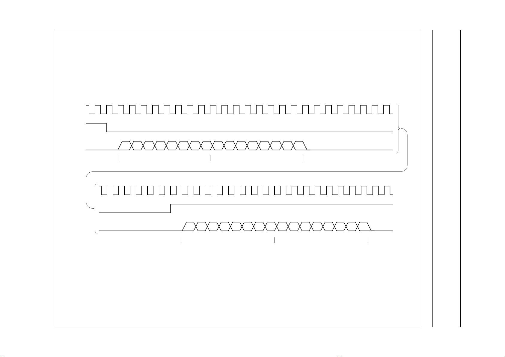
2
The position of the first SB-I
shown in Fig.10.
S-bytes in a tape frame is
February 1994 15

Philips Semiconductors Product specification
Tape formatting and error
correction for the DCC system
SNUM
LTREF
SBWS
SBDA
0
MODE DPAP OR DPAR
MODE DRAR
1
BYTE number
8191
OF PREVIOUS
TAPE FRAME
SAA2022
BYTE number 2
BYTE number 1
BYTE number 0
SNUM
LTREF
SBWS
SBDA
3
BYTE number 8191
OF PREVIOUS
TAPE FRAME
BYTE number 2
BYTE number 1
BYTE number 0
0
Fig.10 Position of first SB-I2S-bytes in tape frame.
MEA701 - 2
February 1994 16
 Loading...