Philips SAA2003H Datasheet

INTEGRATED CIRCUITS
DATA SH EET
SAA2003
Stereo filter and codec
Preliminary specification
File under Integrated Circuits, IC01
Philips Semiconductors
May 1994
Philips Semiconductors Preliminary specification
Stereo filter and codec SAA2003
FEATURES
• Single-chip stereo filter and codec
• Wide operating voltage range: 2.7 to 5.5 V
• Low-power consumption: 98 mW; 3.0 V
• Sleep mode for low power and low Electromagnetic
Interference (EMI)
• Transparent serial audio data mode in sleep
• IEC 958 digital output
• Peak level detector for start of track detection or
VU meter
• Versatile fade processor; slow/fast fade, mute,
12 dB attenuation
2
• Serial audio interface for I
S or EIAJ formats
GENERAL DESCRIPTION
The SAA2003 performs the sub-band filtering and audio
frame codec functions in the Precision Adaptive Sub-band
Coding (PASC) system. It can be used as a stand-alone
decoder for playback only applications, but requires the
addition of an Adaptive Allocation and Scale Factor
processor (SAA2013) in order to perform PASC encoding
in a DCC record system.
• Error concealment
• Three-wire L3 bus microcontroller interface
• Three sample rates:
– 32 kHz
– 44.1 kHz
– 48 kHz
• Internal or external clock source
• Three programmable outputs
• Small surface mounted package (SOT307).
ORDERING INFORMATION
EXTENDED TYPE
NUMBER
SAA2003H 44 QFP
Note
1. When using reflow soldering it is recommended that the Dry Packing instructions in the
Pocketbook”
are followed. The pocketbook can be ordered using the code 9398 510 34011.
PINS PIN POSITION MATERIAL CODE
(1)
PACKAGE
plastic SOT307
“Quality Reference
May 1994 2
Philips Semiconductors Preliminary specification
Stereo filter and codec SAA2003
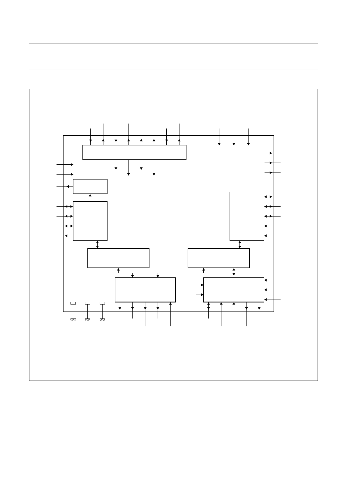
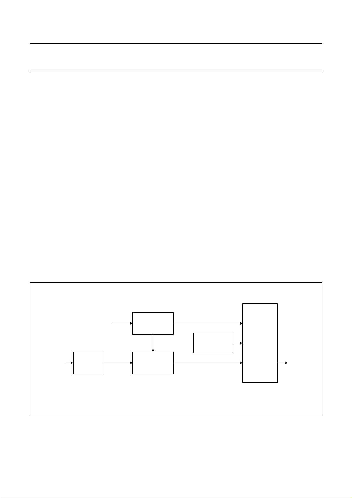
BLOCK DIAGRAM
handbook, full pagewidth
TEST0
TEST1
IECOP
WS
SCK
SD1
SD2
19
20
29
36
35
34
33
X22OUT
X22IN
651094113738 287 39
IEC 958
OUTPUT
BASEBAND
SERIAL
INTERFACE
AND
PEAK
DETECTOR
STEREO SUBBAND
FILTER PROCESSOR
27 8 40
X24OUT
X24IN
CLOCK GENERATOR
FS128
CLK22
6.15 MHz
FS256
43 2 3 44 1
SBMCLK
FILTERED DATA
INTERFACE
CLK24
FS256
X256
SAA2003
V
DD1VDD2VDD3
SUBBAND
SERIAL
INTERFACE
PASC CODEC
PROCESSOR
MICROCONTROLLER
INTERFACE AND CONTROL
17 18 14 15 16 41 42
32
31
30
25
24
23
22
26
21
13
12
MUTEDAC
ATTDAC
DEEMDAC
SBWS
SBCL
SBDA
SBDIR
SBEF
URDA
RESET
SLEEP
MBD618
V
SS1VSS2VSS3
FDCL
FSYNC
FDWS
FDAO
FDAI
Fig.1 Block diagram.
May 1994 3
L3DATA L3MODE SYNCDAILTCNT0
L3CLK FDIRLTCNT1

Philips Semiconductors Preliminary specification
Stereo filter and codec SAA2003
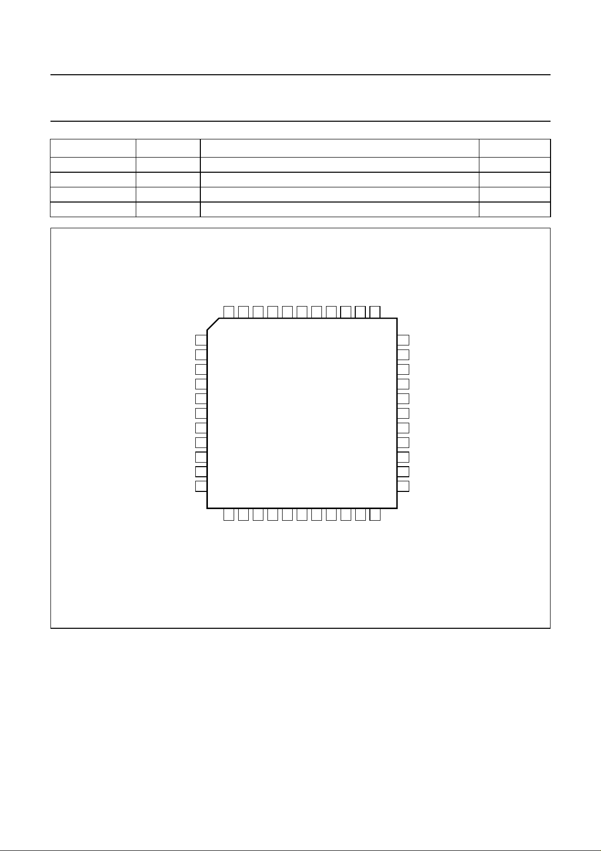
PINNING
SYMBOL PIN DESCRIPTION TYPE
FDAI 1 filtered data input from SAA2013 I
FDCL 2 filtered data bit clock O
FDWS 3 filtered data word select O
CLK22 4 22.5792 MHz buffered clock output O
X22OUT 5 22.5792 MHz crystal output O
X22IN 6 22.5792 MHz crystal input I
V
DD2
V
SS2
X24OUT 9 24.576 MHz crystal output O
X24IN 10 24.576 MHz crystal input I
CLK24 11 24.576 MHz buffered clock output O
SLEEP 12 sleep mode; device inactive I
RESET 13 device reset I
L3DATA 14 3-wire interface; serial data I/O
L3CLK 15 3-wire interface; bit clock I
L3MODE 16 3-wire interface; mode control I
LTCNT0 17 LT interface; control bit 0 I
LTCNT1 18 LT interface; control bit 1 I
TEST0 19 test mode select I
TEST1 20 test mode select I
URDA 21 unreliable data flag from drive processor I
SBDIR 22 sub-band data direction I
SBDA 23 sub-band serial data I/O
SBCL 24 sub-band bit clock I/O
SBWS 25 sub-band word select I/O
SBEF 26 sub-band error flag from drive processor I
V
SS1
V
DD1
IECOP 29 IEC 958 digital audio output O
DEEMDAC 30 DAC control or general purpose output O
ATTDAC 31 DAC control or general purpose output O
MUTEDAC 32 DAC control or general purpose output O
SD2 33 serial audio data to DAC O
SD1 34 serial audio data to/from DAIO and DAC I/O
SCK 35 serial audio data bit clock I/O
WS 36 serial audio data word select I/O
X256 37 master audio clock from external source I
FS256 38 master audio clock at 256 times sample frequency O
V
DD3
V
SS3
7 supply voltage (clock oscillator) −
8 supply ground (clock oscillator) −
27 digital supply ground −
28 digital supply voltage −
39 supply voltage (FS256) −
40 supply ground (FS256) −
May 1994 4
Philips Semiconductors Preliminary specification
Stereo filter and codec SAA2003
SYMBOL PIN DESCRIPTION TYPE
FDIR 41 filter direction; encode or decode O
SYNCDAI 42 settings synchronization for DAIO O
FSYNC 43 sub-band 0 sample synchronization for SAA2013 O
FDAO 44 filtered data output to SAA2013 O
SS3
FDAO
44
FSYNC
SYNCDAI
43
42
FDIR
41
DD3
FS256
V
40
X256
V
39
38
37
WS
36
SCK
35
SD1
34
FDAI
FDCL
FDWS
CLK22
X22OUT
X22IN
V
DD2
V
SS2
X24OUT
X24IN
CLK24
1
2
3
4
5
6
7
8
9
10
11
12
13
SLEEP
RESET
14
15
L3CLK
L3DATA
SAA2003
16
17
LTCNT0
L3MODE
18
19
TEST0
LTCNT1
20
TEST1
21
URDA
22
SBDIR
SD2
33
MUTEDAC
32
ATTDAC
31
DEEMDAC
30
IECOP
29
V
28
V
27
26
SBEF
SBWS
25
SBCL
24
23
SBDA
MBD619
DD1
SS1
Fig.2 Pin configuration.
May 1994 5
May 1994 6
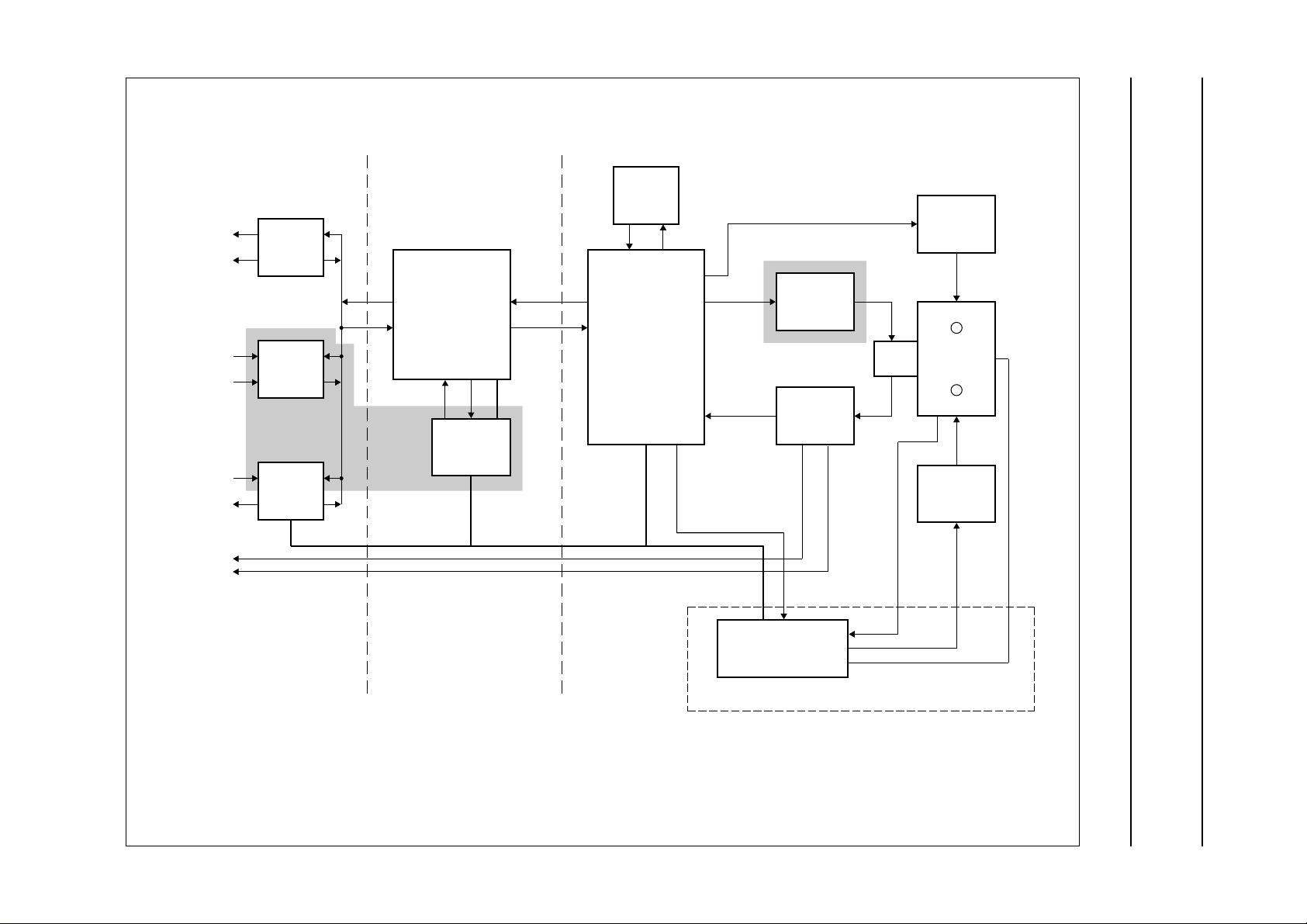
FUNCTIONAL DESCRIPTION
Philips Semiconductors Preliminary specification
Stereo filter and codec SAA2003
RAM
41464
analog
output
analog
input
IEC958
analog CC
L output
analog CC
R output
L
DAC
TDA1305
R
SFC3
SAA2003
STEREO
FILTER CODEC
2
ADAS3
SAA2013
ADAPTIVE
ALLOCATION
L
R
baseband
I S
ADC
SAA7366
DIGITAL
AUDIO I/O
TDA1315
2
filtered I S
AUDIO IN/OUT PASC PROCESSOR
sub-band
2
I S
BUFFER
64K x 4
DRP
SAA2023
OR
SAA3323
DRIVE
PROCESSOR
search data
TAPE DRIVE PROCESSING
speed control
WRAMP
TDA1381
WRITE AMP.
RDAMP
TDA1380
READ AMP.
FIXED
HEAD
CAPSTAN
DRIVE
TAPE
MECHANICS
DRIVERS
detect
switch
Fig.3 DCC system block diagram.
handbook, full pagewidth
SYSTEM
MICROCONTROLLER
SYSTEM CONTROL
MBD620
Philips Semiconductors Preliminary specification
Stereo filter and codec SAA2003
PASC processor
The PASC processor is a dedicated Digital Signal
Processor (DSP) engine which efficiently codes digital
audio data at a bit rate of 384 kbits/s without affecting the
sound quality. This is achieved using an efficient adaptive
data notation and by only encoding the information which
can be heard by the human ear.
The audio data is split into 32 equal sub-bands during
encoding. For each of the sub-bands a masking threshold
is calculated. The samples from each of the sub-bands are
included in the PASC data with an accuracy that is
determined by the available bit-pool and by the difference
between the signal power and the masking threshold for
that sub-band.
The stereo filter codec performs the splitting (encoding)
and reconstruction (decoding), including the necessary
formatting functions. During encoding, the adaptive
allocation and scaling circuit calculates the required
accuracy (bit allocation) and scale factors of the sub-band
samples.
E
NCODING (SEE FIG.4)
The incoming serial audio data is filtered into 32 sub-bands
for left and right (I and II) channels using the stereo filter
part of the SAA2003. A PASC frame is made up of left and
right (I and II) audio data for 12 samples from each of the
32 sub-bands, a total of 768 audio samples. For every
PASC frame the SAA2013 calculates a bit allocation and
scale factor table which is transferred to the SAA2003. All
the samples in a frame are scaled in accordance with the
scale factor calculated by the SAA2013. Once scaled the
samples are re-quantized to reduce the number of bits to
correspond with the allocation table calculated by the
SAA2013. Synchronization, allocation and scale factor
information is then added to provide a fully encoded PASC
data signal. These frames of data are then sent to the drive
processor IC (SAA2023 or SAA3323).
DECODING (SEE FIG.5)
In decoding mode the SAA2003 synchronizes and
recovers frames of data from the drive processor. The
recovered allocation data and the scale factors are used to
correctly re-quantize and re-scale the PASC sub-band
samples. The decoded sub-band samples, which are
represented in 24-bits two’s complement notation, are
reconstructed by the sub-band filters into a single
complete digital audio signal.
handbook, full pagewidth
ALLOCATION AND
SCALE FACTOR
INFORMATION
TABLE
SCALING AND
QUANTI ZATION
baseband
samples
from SAA2013
SUB-BAND
FILTER
sub-band
samples
Fig.4 Encoding mode.
May 1994 7
allocation information
and scale factor indices
SYNC AND
CODING
INFORMATION
quantified samples
FORMATTER
PASC
OUTPUT
DATA
MLB764

Philips Semiconductors Preliminary specification
Stereo filter and codec SAA2003
handbook, full pagewidth
PASC
data
input
FORMATTER
DE–
sync/coding
allocation
scale factor
quantified
samples
CONTROL
SCALE
FACTOR
ARRAY
AND ALLOCATION
DE-QUANTIZATION
MULTIPLY
OUTPUT
CONTROL
sub-band
samples
MEA804 - 1
SUB-BAND
FILTER
baseband
samples
Fig.5 Decoding mode.
Crystal oscillators
The recommended crystal oscillator configuration is shown in Fig.6. The specified component values only apply to
crystals with a low equivalent series resistance of <40 Ω.
C2 33 pF
C1 33 pF
C3 33 pF
C4 33 pF
22.5792
MHz
X1
24.576
MHz
X2
R1
1 MΩ
R2 220Ω
R4
1 MΩ
R3 1 kΩ
X22IN
X22OUT
X24IN
X24OUT
40
41
42
43
SAA2003
MBD621
Fig.6 Crystal oscillator components.
System reset
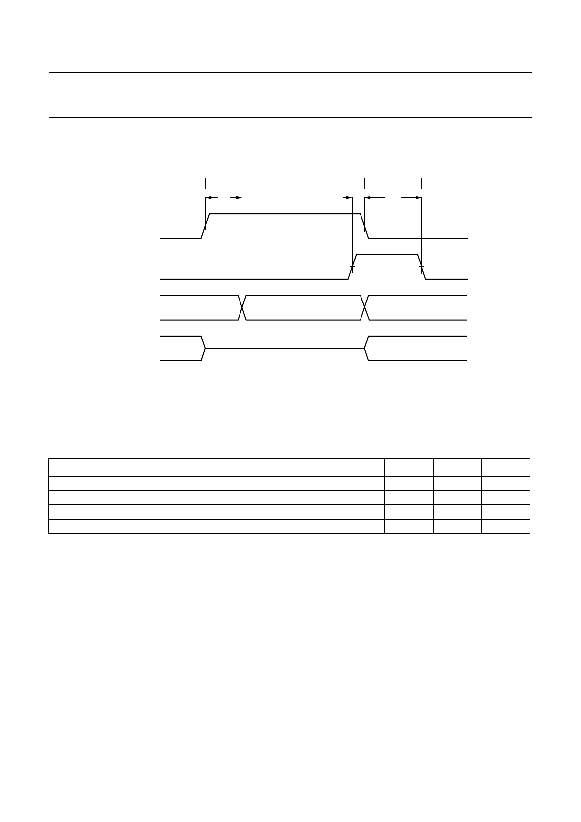
Reset must be active from system power-up for >1 ms. Reset must also be active for >1 ms after the falling edge of sleep
as shown in Fig.7.
May 1994 8
Philips Semiconductors Preliminary specification
Stereo filter and codec SAA2003
handbook, full pagewidth
STANDBY
RESET
CLK24/CLK22
I/O's
ACTIVE
MODE 1 MODE 2 MODE 3 MODE 4
t
1
ACTIVE
Fig.7 Reset and sleep timing.
Table 1 Reset and sleep timing modes (see Fig.7).
t
2
t
3
ACTIVESTATIC
ACTIVE
MBD622
MODE DESCRIPTION TIMING MIN. MAX. UNIT
MODE1 standby stage 1; clocks still running t
MODE2 standby mode; clocks stopped t
MODE3 clocks running; reset active t
1
2
3
400 − ns
0 − ns
1 − ms
MODE4 normal operational mode −−−
Sleep mode
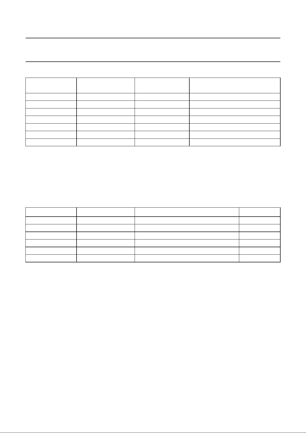
A HIGH input applied to the SLEEP pin halts all internally generated clock signals. If the transparent mode of the serial
audio interface is set before entering sleep, the data at the X256 external clock input is sent to the FS256 output and the
data at SD1 input is sent to the SD2 output. If transparent mode is not set, these two outputs are high impedance during
sleep mode.
The IECOP pin is set to high impedance during sleep mode, unless the transparent mode is selected and WS-SEL is set.
May 1994 9
Philips Semiconductors Preliminary specification
Stereo filter and codec SAA2003
Table 2 Transparent mode function in sleep.
PIN
TRANSPARENT
(1)
MODE
WS-SEL
(2)
PIN FUNCTION
FS256 1 X FS256
FS256 0 X high impedance
SD2 1 X SD1
SD2 0 X high impedance
IECOP 0 X high impedance
IECOP 1 0 high impedance
IECOP 1 1 WS
Notes
1. Transparent mode is controlled by bit 3 of the serial audio data interface mode control register.
2. WS-SEL is controlled by bit 3 of the codec extended settings register.
Serial audio interface
The signals between the SAA2003 and the serial audio input/output are shown in Table 3.
Table 3 Interface signals between SAA2003 and serial audio input/output.
PIN INPUT/OUTPUT FUNCTION FREQUENCY
WS bi-directional audio data word select f
SCK bi-directional audio data bit clock 64f
SD1 bi-directional serial audio data to/from DAIO and ADC −
SD2 output audio serial data to DAC −
FDIR output PASC mode encode/decode −
IECOP output alternative serial data word select for SD2 −
s
s
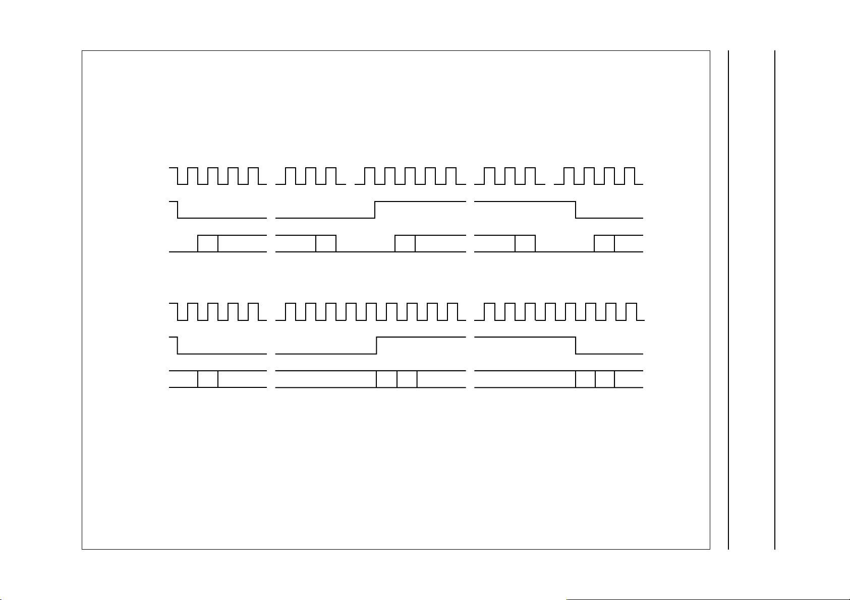
The word select (WS) line indicates the channel being transmitted (either left or right; I or II) and is equal in frequency to
the sampling frequency (f
).
s
Operating at a frequency of 64 × fs, the bit clock (SCK) dictates that each WS period contains 64 SD1 or SD2 data bits.
Of these bits a maximum of 36 are used to transfer data (samples may have a length up to 18 bits). Samples are
transferred most significant bit (MSB) first. Both WS and SD1/SD2 change state at the negative edge of SCK.
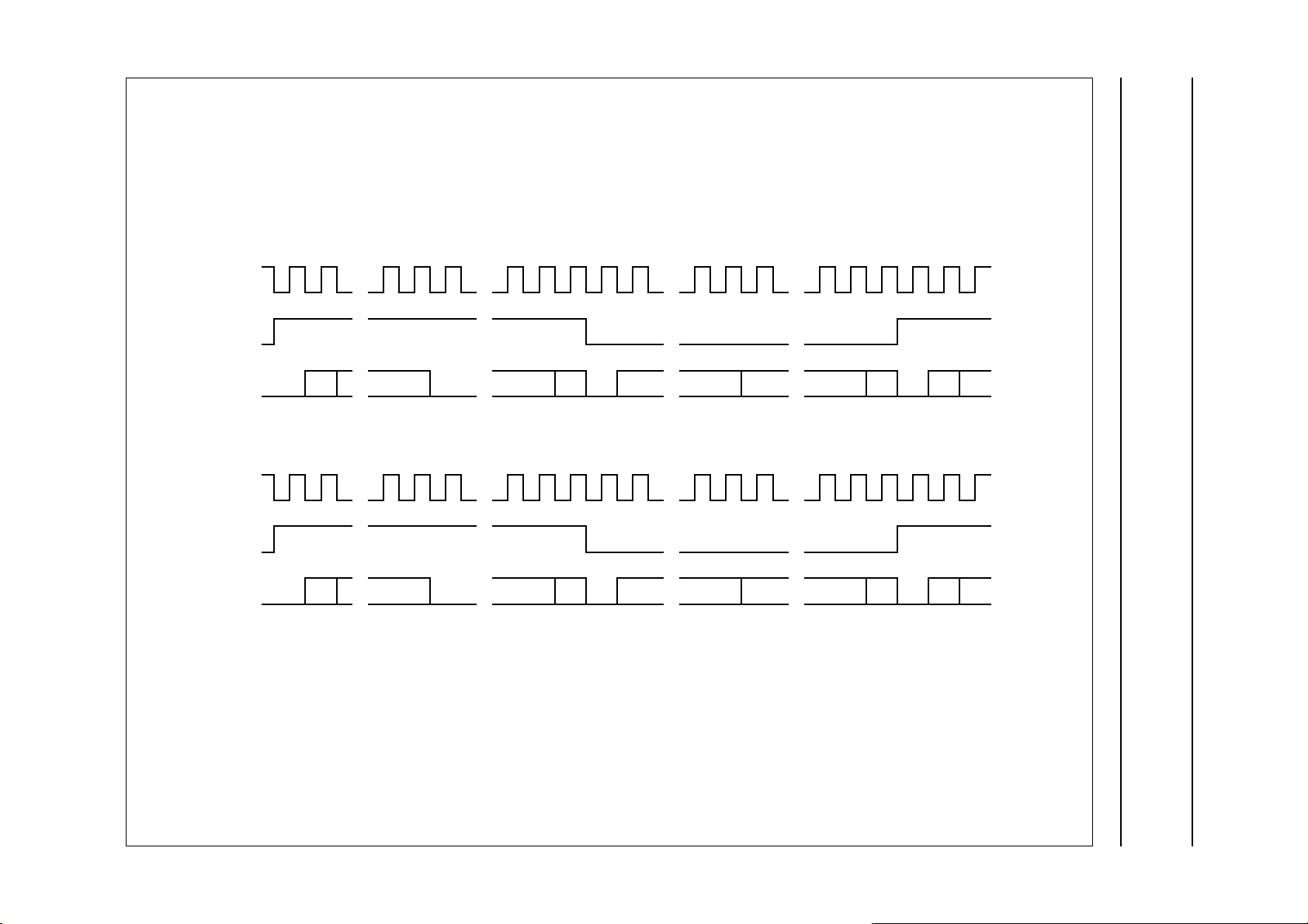
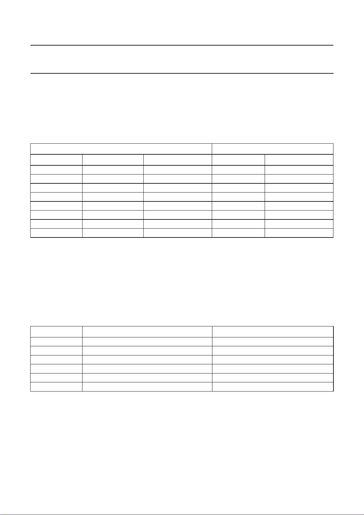
The serial audio data is transferred between the SAA2003 and the input/output using either the standard I2S (default) as
shown in Fig.8 or the EIAJ format as shown in Fig.9.
May 1994 10
May 1994 11
Philips Semiconductors Preliminary specification
Stereo filter and codec SAA2003
0123 17 18 32 33 34 3531 49 50 63012
SCL
SWS
SD1/
SD2
0123 12 13 16 17 18 1915 28 29 31012
SCL
SWS
SD1/
SD2
a. Master and slave modes; 18 bits.
b. Slave mode only; 16 bits.
MSB
left channel data right channel data
LSB
MSB
a.
14 30
left channel data right channel data
b.
LSB
LSB
MSB
MSBLSB MSBMSB
MBD623
Fig.8 Serial audio interface SD1/SD2; I2S data format.
May 1994 12
Philips Semiconductors Preliminary specification
Stereo filter and codec SAA2003
SCL
SWS
SD1/
SD2
SCL
SWS
SD1/
SD2
012 14 15 30 31 32 33 46 47 62 63 0 1
left channel data right channel data
MSB MSB LSB MSB
LSB MSBMSB
a.
012 16 17 30 31 32 33 48 49 62 63 0 1
left channel data right channel data
MSB MSB LSB MSB
LSB MSBMSB
b.
2
2
MBD624
a. Master mode; 18 bits.
b. Master mode (EIAJ); 16 bits.
Fig.9 Serial audio interface SD1; EIAJ data format.
Philips Semiconductors Preliminary specification
Stereo filter and codec SAA2003
SERIAL AUDIO INTERFACE DATA FORMATS IN ENCODING MODE
In encoding mode, the serial audio data input for the PASC processor is taken from the SD1 pin. This data is scaled by
the fade processor before being sent to the PASC processor. The output from the fade processor is sent in parallel to
the SD2 output.
Both I2S and EIAJ formats are supported.
Table 4 Serial audio data interface formats in encoding mode.
SD1 INPUT SD2 OUTPUT
FORMAT MASTER/SLAVE RESOLUTION FORMAT RESOLUTION
I2S master 18 bit I2S 18 bit
2
I
S slave 18 bit I2S 18 bit
2
I
S master 16 bit I2S 18 bit
2
S slave 16 bit I2S 16 bit
I
EIAJ
EIAJ
EIAJ
EIAJ
(1)
(1)
(1)
(1)
master 18 bit I2S 18 bit
slave 18 bit I2S 18 bit
master 16 bit I2S 18 bit
slave 16 bit I2S 18 bit
Note
1. If SD1 is used in EIAJ mode, and the data from SD2 is required, the IECOP can be re-programmed to provide a
suitable I
S
ERIAL AUDIO INTERFACE DATA FORMATS IN DECODING MODE
2
S WS signal for SD2. The IEC 958 output is not available in this mode.
In decoding mode, the output from the PASC processor, connected via the fade processor, is present at both SD1 and
SD2.
Both I2S and EIAJ formats are supported.
Table 5 SD1/SD2 output decoding formats.
FORMAT MASTER/SLAVE RESOLUTION
(1)
I2S master 18 bit
2
S slave 18 bit
I
2
I
S master 16 bit
2
I
S slave 16 bit
EIAJ master 18 bit
EIAJ master 16 bit
Note
1. The sub-band filter performs rounding to 16 or 18 bits according to the operating mode of the interface.
ERIAL AUDIO INTERFACE MODE CONTROL
S
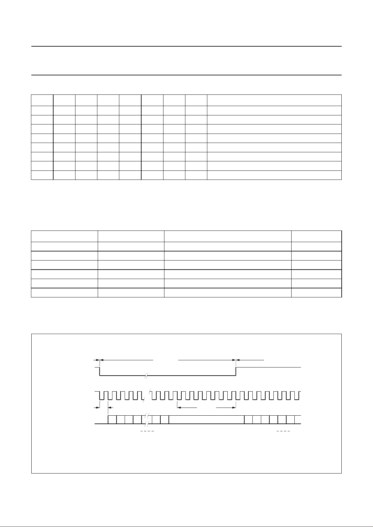
The operating mode of the interface is programmed by the extended settings registers as shown in Table 6.
May 1994 13
Philips Semiconductors Preliminary specification
Stereo filter and codec SAA2003
Table 6 Extended settings register.
A3 A2 A1 A0 D3 D2 D1 D0 MODE
0 0 1 0 X X X 0 16 bit operation; 16 bit rounding
0 0 1 0 X X X 1 18 bit operation; 18 bit rounding
2
0010XX0XI
0 0 1 0 X X 1 X EIAJ data format
0 0 1 0 X 0 X X peak detector input SD1
0 0 1 0 X 1 X X peak detector input SD2
0 0 1 0 0 X X X SD1/FS256 transparent mode disabled
0 0 1 0 1 X X X SD1/FS256 transparent mode enabled
Filtered data interface
The filtered data interface transfers the sub-band filtered data between the stereo filter codec and adaptive allocation and
scaling parts of the DCC chip-set, and consists of the signals as shown in Table 7.
S data format
Table 7 Filtered data interface signals.
PIN INPUT/OUTPUT FUNCTION FREQUENCY
FDCL output filtered data bit clock 64f
FDWS output filtered data word select f
s
s
FDAO output filtered data serial output −
FDAI input filtered data serial input −
FDIR output decode/encode control −
FSYNC output filtered data sync signal; band zero −
ILTERED DATA INTERFACE FORMAT
F
The filtered data is transferred over the interface in accordance with the formats illustrated in Figs 10 and 11.
handbook, full pagewidth
channel
FDWS
FDCL
left 32 bits
right
1
FDAI/
FDAO
bit :
2322212
MSB LSB
02010
0
0
Fig.10 Transfer of filtered data; SAA2003/SAA2013.
May 1994 14
7 bits
2322212
MSB
0
MLB765
 Loading...