

Philips saa1575hl DATASHEETS

INTEGRATED CIRCUITS
DATA SH EET
SAA1575HL
Global Positioning System (GPS)
baseband processor
Product specification
Supersedes data of 1999 May 17
File under Integrated Circuits, IC18
1999 Jun 04

Philips Semiconductors Product specification
Global Positioning System (GPS)
baseband processor
CONTENTS
1 FEATURES
2 GENERAL DESCRIPTION
3 QUICK REFERENCE DATA
4 ORDERING INFORMATION
5 BLOCK DIAGRAM
6 PINNING
7 FUNCTIONAL DESCRIPTION
7.1 Overview
7.2 The 80C51XA processor
7.3 The GPS correlators
7.4 Memory organization
7.4.1 Data memory space
7.4.2 Code memory space
7.5 CPU peripheral features
7.5.1 Timers/counters
7.5.2 Watchdog timer
7.5.3 UARTs
7.5.4 RF IC programming port
7.5.5 General purpose I/O
7.6 The real-time clock
7.7 The external bus
7.7.1 Program memory chip select
7.7.2 Data memory chip select
7.7.3 Read strobe
7.7.4 Write LOW byte strobe
7.7.5 Write HIGH byte strobe
7.8 Backup supplies and reset
7.8.1 Supply domains
7.8.2 Power-down design strategy
7.8.3 System reset control
7.8.4 Power saving modes
7.9 Clock signals and oscillators
7.9.1 System clock (XTAL1)
7.9.2 RTC clock (XTAL3)
7.9.3 Reference clock (RCLK)
SAA1575HL
8 LIMITING VALUES
9 THERMAL CHARACTERISTICS
10 DC CHARACTERISTICS
11 AC CHARACTERISTICS
12 DEFAULT APPLICATION AND
DEMONSTRATION BOARD
13 PACKAGE OUTLINE
14 SOLDERING
14.1 Introduction to soldering surface mount
packages
14.2 Reflow soldering
14.3 Wave soldering
14.4 Manual soldering
14.5 Suitability of surface mount IC packages for
wave and reflow soldering methods
15 DEFINITIONS
16 LIFE SUPPORT APPLICATIONS
1999 Jun 04 2

Philips Semiconductors Product specification
Global Positioning System (GPS)
baseband processor
1 FEATURES
• Single-chip GPS baseband solution with built-in 16-bit
microcontroller
• All digital, 0.5 micron CMOS technology
• Single power supply with full 3 V operation
• Separate I/O power supply pins for operation with
3 or 5 V external devices
• Up to 30 MHz system clock from on-chip crystal
oscillator or external clock input
• 2 kbytes words internal data memory for fast execution
• External bus for up to 512 kbytes words data memory
and 512 kbytes words program memory
• Programmable external bus timing to match external
memory speed
• Chip selection outputs to reduce glue logic requirements
• Reset controller for power-down detection and servicing
• 8 GPS channel correlators driven by firmware for
flexible GPS correlation algorithms
• 1 second pulse output of GPS time
• 2-bit digital IF GPS signal input synchronized to external
sample clock
• 2 fully duplex UARTs for communication with host
system processor and other devices
• Real-time clock with 32.768 kHz crystal and supply for
low power timekeeping
• Watchdog timer
• Power-down modes under firmware control
• 100-pin LQFP package
• 50 mA supply current (typ.) when 8 GPS channels in
track (approximate).
SAA1575HL
However, for compatibility with current automotive
applications, the periphery is supplied from separate pins
and can be operated between 3 and 5 V, as required.
The function of the SAA1575HL is to read the 1 or 2-bit
sampled IF bitstream from a front-end IC and, under
control of firmware on an external ROM, calculate the full
GPS solution. The results are communicated to a host in
National Maritime Electronics Association (NMEA) format
via a standard serial port. A second serial port can be used
to provide differential GPS information to the processor for
more advance applications. In addition, various other
functions are integrated onto the IC such as a real-time
GPS clock, a power-down/reset controller, timer/counters
and a watchdog timer.
To summarise, the SAA1575HL has the following
functional units:
• 16-bit 80C51XA microcontroller core
• 2 kbytes words on-chip SRAM (16-bit words)
• 8 GPS channel correlators
• 2 UARTs
• 8 general purpose I/O lines
• 3 timer/counters
• 1 real-time clock
• 1 watchdog timer
• 1 power-down/reset controller.
The structure is based on a 16-bit microcontroller core
operating on all other units as memory mapped
peripherals and registers. A 16-bit data bus and a 19-bit
address bus are extended to external pins so that external
data and program memory can be accessed. On-chip
decoder circuits eliminate the need for external glue logic
for external memory access.
2 GENERAL DESCRIPTION
The SAA1575HL is an integrated circuit which implements
a complete baseband function for Global Positioning
System (GPS) receivers. It combines a 16-bit Philips
80C51XA microcontroller, 8 GPS channel correlators and
related peripherals in a single IC. Users can implement a
complete GPS receiver using only the SAA1575HL, the
UAA1570HL front-end Philips IC (or similar), external
memory and a few discrete components.
The IC is aimed at low cost applications. A low power
solution was also used where possible, although this was
of secondary importance to cost. The core of the
SAA1575HL operates at 3 V.
1999 Jun 04 3
Each of the 8 GPS channel correlators includes a carrier
Numerically Controlled Oscillator (NCO), PN code
generator, phase rotator and low-pass filter. They
correlate the local PN sequence with the digitized input
GPS signal and generate the filtered correlation result for
the microcontroller. The firmware provided then generates
a navigation solution and provides standard GPS data
outputs to the user.
Philips Semiconductors Product specification
Global Positioning System (GPS)
SAA1575HL
baseband processor
The GPS firmware is located in off-chip program memory. It processes the GPS signals from up to 8 satellites and
generates GPS information that can be output to the host processor through one of the two serial ports. Much of
hardware configuration of the SAA1575HL can be controlled by the firmware and so details such as the external bus
timing may change between firmware revisions. For the purpose of this document, the standard Philips firmware has
been assumed (release HD00).
3 QUICK REFERENCE DATA
SYMBOL PARAMETER CONDITIONS MIN. TYP. MAX. UNIT
V
CC(core)
V
CC(P)
V
CC(R)
V
CC(B)
I
CC(core)
I
CC(R)
I
CC(B)
I
CC(P)
f
osc
T
amb
core supply voltage 2.7 3.3 3.6 V
peripheral supply voltage 2.7 5.0 5.5 V
real-time clock core supply voltage 2.4 3.3 3.6 V
backup peripheral supply voltage 2.7 5.0 5.5 V
core supply current normal mode − 35 − mA
sleep mode − 15 − mA
real-time clock core supply current f
backup peripheral supply current normal mode; dependent on
= 32.768 kHz − 10 30 µA
RTC
− 5 − mA
load
sleep mode − 1 −µA
peripheral supply current normal mode − 20 − mA
sleep mode −−1mA
oscillator frequency 26 30 32 MHz
ambient temperature −40 +25 +85 °C
4 ORDERING INFORMATION
TYPE
NUMBER
NAME DESCRIPTION VERSION
PACKAGE
SAA1575HL LQFP100 plastic low profile quad flat package; 100 leads; body 14 × 14 × 1.4 mm SOT407-1
1999 Jun 04 4
Philips Semiconductors Product specification
Global Positioning System (GPS)
baseband processor
5 BLOCK DIAGRAM
handbook, full pagewidth
80C51XA PROCESSOR MODULE
STATIC RAM
(2 kbytes WORDS)
XTAL1
XTAL2
14
15
SYSTEM CLOCK
GENERATOR
ADDRESS
80C51XA
CORE
AND
DATA
UART 0
UART 1
TIMER 0, 1
TIMER 2
WATCHDOG
TIMER
SAA1575HL
83
TXD0
84
RXD0
81
TXD1
82
RXD1
D15 to D0
WRH
WRL
RD
IF1
IF2
RCLK
SCLK
T1S
TEST1
TEST2
48, 49, 53 to 59, 62 to 64, 67 to 70
45
46
47
93
CORRELATORS
92
98
1
2
99
100
n.c.
CONTROL
CHANNEL 0
CHANNEL 2
CHANNEL 4
CHANNEL 6
8, 9
97
72 80
V
CC(R)VCC(B)
CHANNEL 1
CHANNEL 3
CHANNEL 5
CHANNEL 7
V
12, 30,
66
CC(core)
EXTERNAL BUS
INTERFACE
SAA1575HL
16, 25,
37, 51,
61, 86
V
CC(P)
V
10, 11, 18 to 24, 27 to 29, 32 to 36, 39, 40
CONTROL
REGISTERS
REAL-TIME
CLOCK
RESET
CONTROLLER
13, 17, 26, 31,
38, 50, 60, 65,
71, 79, 85
SS
4 34244
TP3TP4
5 to 7, 87, 88,
94 to 96
TP2
TP1
41
73
89
90
91
76
75
74
52
43
78
77
A19 to A1
PMCS
DMCS
RFDAT
RFCLK
RFLE
GPIO7 to GPIO0
XTAL3
XTAL4
PWRFAIL
PWRDN
RSTIME
PWRM
PWRB
MHB460
Fig.1 Block diagram.
1999 Jun 04 5
Philips Semiconductors Product specification
Global Positioning System (GPS)
SAA1575HL
baseband processor
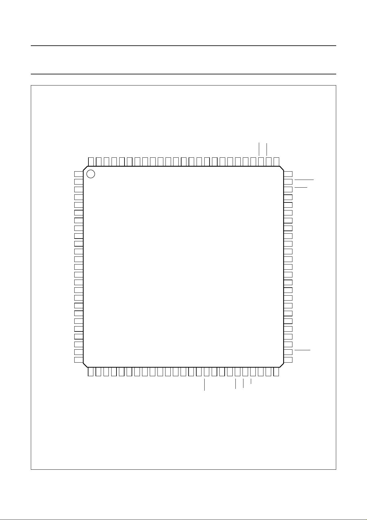
6 PINNING
SYMBOL PIN I/O DESCRIPTION
SCLK 1 O Sample clock: sample clock generated internally by dividing down the RCLK
(reference clock) input. This output is provided for use by the front-end IC.
T1S 2 O GPS time pulse: a 1 pulse per second output whose rising or falling edge (firmware
controlled) is synchronized to GPS time when the receiver is tracking a GPS signal.
The pulse length is approximately 1 ms.
TP3 3 I Test pin: tie HIGH
TP4 4 I Test pin: tie HIGH
GPIO5 5 I/O GPIO bit 5: standard general purpose I/O mapped into the segment 15 of the address
space. The top 4 bits can be used as the XA external timer control access pins
(T0, T1, T2 and T2EX).
GPIO6 6 I/O GPIO bit 6: standard general purpose I/O mapped into the segment 15 of the address
space. The top 4 bits can be used as the XA external timer control access pins
(T0, T1, T2 and T2EX).
GPIO7 7 I/O GPIO bit 7: standard general purpose I/O mapped into the segment 15 of the address
space. The top 4 bits can be used as the XA external timer control access pins
(T0, T1, T2 and T2EX).
n.c. 8 O Not connected: do not connect
n.c. 9 O Not connected: do not connect
A19 10 O External memory address bus bit 19: 19-bit address bus; used to address external
RAM and program memory
A18 11 O External memory address bus bit 18: 19-bit address bus; used to address external
RAM and program memory
V
CC(core)
V
SS
XTAL1 14 I Crystal 1: input to the inverting amplifier; used in the system oscillator circuit and
XTAL2 15 O Crystal 2: output from the system oscillator amplifier
V
CC(P)
V
SS
A17 18 O External memory address bus bit 17: 19-bit address bus; used to address external
A16 19 O External memory address bus bit 16: 19-bit address bus; used to address external
A15 20 O External memory address bus bit 15: 19-bit address bus; used to address external
A14 21 O External memory address bus bit 14: 19-bit address bus; used to address external
A13 22 O External memory address bus bit 13: 19-bit address bus; used to address external
A12 23 O External memory address bus bit 12: 19-bit address bus; used to address external
12 − Main core power supply: 2.7 to 3.6 V only; main supply for the core in normal
operation
13 − Ground: 0 V reference
input to the internal clock generator circuits
16 − Main I/O power supply: 2.7 to 5.5 V operating range; main supply for the periphery
in normal operation
17 − Ground: 0 V reference
RAM and program memory
RAM and program memory
RAM and program memory
RAM and program memory
RAM and program memory
RAM and program memory
1999 Jun 04 6
Philips Semiconductors Product specification
Global Positioning System (GPS)
SAA1575HL
baseband processor
SYMBOL PIN I/O DESCRIPTION
A11 24 O External memory address bus bit 11: 19-bit address bus; used to address external
RAM and program memory
V
CC(P)
V
SS
A10 27 O External memory address bus bit 10: 19-bit address bus; used to address external
A9 28 O External memory address bus bit 9: 19-bit address bus; used to address external
A8 29 O External memory address bus bit 8: 19-bit address bus; used to address external
V
CC(core)
V
SS
A7 32 O External memory address bus bit 7: 19-bit address bus; used to address external
A6 33 O External memory address bus bit 6: 19-bit address bus; used to address external
A5 34 O External memory address bus bit 5: 19-bit address bus; used to address external
A4 35 O External memory address bus bit 4: 19-bit address bus; used to address external
A3 36 O External memory address bus bit 3: 19-bit address bus; used to address external
V
CC(P)
V
SS
A2 39 O External memory address bus bit 2: 19-bit address bus; used to address external
A1 40 O External memory address bus bit 1: 19-bit address bus; used to address external
PMCS 41 O External program memory select: external program memory read strobe
TP2 42 I Test pin: tie LOW
RSTIME 43 I Reset timer control: this controls the on-chip reset timer. If this is HIGH, reset will be
TP1 44 I Test pin: tie LOW
WRH 45 I/O Write MSB: write strobe for external data memory; asserted for both MSB and word
WRL 46 I/O Write LSB: write strobe for external data memory; asserted for both LSB and word
RD 47 I/O External data read: read strobe for external data memory; input mode only used for
25 − Main I/O power supply: 2.7 to 5.5 V operating range; main supply for the periphery
in normal operation
26 − Ground: 0 V reference
RAM and program memory
RAM and program memory
RAM and program memory
30 − Main core power supply: 2.7 to 3.6 V only; main supply for the core in normal
operation
31 − Ground: 0 V reference
RAM and program memory
RAM and program memory
RAM and program memory
RAM and program memory
RAM and program memory
37 − Main I/O power supply: 2.7 to 5.5 V operating range; main supply for the periphery
in normal operation
38 − Ground: 0 V reference
RAM and program memory
RAM and program memory
de-asserted approximately 10 ms after both PWRDN and PWRFAIL go HIGH. If this
is LOW, reset will be de-asserted approximately 10 µs after both
PWRDN and PWRFAIL go HIGH.
write operations; input mode only used for test purposes
write operations; input mode only used for test purposes
test purposes
1999 Jun 04 7
Philips Semiconductors Product specification
Global Positioning System (GPS)
SAA1575HL
baseband processor
SYMBOL PIN I/O DESCRIPTION
D15 48 I/O External memory data bus: 16-bit data bus; used to connect to external RAM and
program memory
D14 49 I/O External memory data bus bit 14: 16-bit data bus; used to connect to external RAM
and program memory
V
SS
V
CC(P)
PWRDN 52 I Power-down indicator: a LOW on this pin asserts an XA interrupt intended for use
D13 53 I/O External memory data bus bit 13: 16-bit data bus; used to connect to external RAM
D12 54 I/O External memory data bus bit 12: 16-bit data bus; used to connect to external RAM
D11 55 I/O External memory data bus bit 11: 16-bit data bus; used to connect to external RAM
D10 56 I/O External memory data bus bit 10: 16-bit data bus; used to connect to external RAM
D9 57 I/O External memory data bus bit 9: 16-bit data bus; used to connect to external RAM
D8 58 I/O External memory data bus bit 8: 16-bit data bus; used to connect to external RAM
D7 59 I/O External memory data bus bit 7: 16-bit data bus; used to connect to external RAM
V
SS
V
CC(P)
D6 62 I/O External memory data bus bit 6: 16-bit data bus; used to connect to external RAM
D5 63 I/O External memory data bus bit 5: 16-bit data bus; used to connect to external RAM
D4 64 I/O External memory data bus bit 4: 16-bit data bus; used to connect to external RAM
V
SS
V
CC(core)
D3 67 I/O External memory data bus bit 3: 16-bit data bus; used to connect to external RAM
D2 68 I/O External memory data bus bit 2: 16-bit data bus; used to connect to external RAM
D1 69 I/O External memory data bus bit 1: 16-bit data bus; used to connect to external RAM
D0 70 I/O External memory data bus bit 0: 16-bit data bus; used to connect to external RAM
V
SS
50 − Ground: 0 V reference
51 − Main I/O power supply: 2.7 to 5.5 V operating range; main supply for the periphery
in normal operation
as a power fail interrupt. Once reset is asserted, either by PWRF AIL or the firmware, it
will remain asserted until a set time after this pin goes HIGH.
and program memory
and program memory
and program memory
and program memory
and program memory
and program memory
and program memory
60 − Ground: 0 V reference
61 − Main I/O power supply: 2.7 to 5.5 V operating range; main supply for the periphery
in normal operation
and program memory
and program memory
and program memory
65 − Ground: 0 V reference
66 − Main core power supply: 2.7 to 3.6 V only; main supply for the core in normal
operation
and program memory
and program memory
and program memory
and program memory
71 − Ground: 0 V reference
1999 Jun 04 8
Philips Semiconductors Product specification
Global Positioning System (GPS)
SAA1575HL
baseband processor
SYMBOL PIN I/O DESCRIPTION
V
CC(R)
DMCS 73 O External data memory select: external RAM select pin, active LOW when the
PWRFAIL 74 I Power fail indicator: a LOW on this pin forces the embedded microcontroller into
XTAL4 75 O Crystal 4: output from the RTC oscillator amplifier; this pin is only 3 V tolerant
XTAL3 76 I Crystal 3: input to inverting amplifier used in the RTC oscillator circuits (32.768 kHz);
PWRB 77 O Backup supply select: this output is intended to drive an external FET used to switch
PWRM 78 O Main supply select: this output is intended to drive an external FET used to switch
V
SS
V
CC(B)
TXD1 81 O Transmitter output 1: transmit channel for serial port 1 (UART1) of the embedded
RXD1 82 I Receiver input 1: receive channel for serial port 1 (UART1) of the embedded
TXD0 83 O Transmitter output 0: transmit channel for serial port 0 (UART0) of the embedded
RXD0 84 I Receiver input 0: receive channel for serial port 0 (UART0) of the embedded
V
SS
V
CC(P)
GPIO4 87 I/O GPIO bit 4: standard general purpose I/O mapped into the segment 15 of the address
GPIO3 88 I/O GPIO bit 3: standard general purpose I/O mapped into the segment 15 of the address
RFDAT 89 O RFIC set-up data: serial data output used to set up the UAA1570HL front-end IC.
RFCLK 90 O RFIC set-up data: clock output for the serial data output used to set up the
72 − Backup core power supply: 2.4 to 3.6 V only. Separate from the core supply to allow
a low capacity battery to be used to maintain the Real-Time Clock (RTC) function.
This should be powered from the main supply during normal operation and switched
to battery backup when the main supply fails.
external data memory space is addressed. This output is driven from V
V
supplies to ensure that the external RAM is not enabled during power-down.
CC(B)
CC(R)
and
reset. Reset will not be de-asserted until a set time after both PWRDN and PWRFAIL
go HIGH. For correct start-up, this pin should be LOW on power-up.
this pin is only 3 V tolerant
the battery backup supply(s). It is active LOW and is controlled directly by the
PWRFAIL.
the main supply(s). It is active LOW and is controlled directly by PWRFAIL.
79 − Ground: 0 V reference
80 − Backup I/O power supply: 2.4 to 5.5 V only. Supply for the RAM select, power fail
and power switching I/O pads only allowing these functions to be powered when the
main power supply fails. This should be powered from the main supply during normal
operation and switched to battery backup when the main supply fails.
processor
processor. It is intended that this serial port is dedicated to differential GPS
information (dependent on firmware).
processor.
processor. It is intended that this serial port is dedicated to the NMEA data stream
(dependent on firmware).
85 − Ground: 0 V reference
86 − Main I/O power supply: 2.7 to 5.5 V operating range; main supply for the periphery
in normal operation
space. The top 4 bits can be used as the XA external timer control access pins
(T0, T1, T2 and T2EX).
space. The top 4 bits can be used as the XA external timer control access pins
(T0, T1, T2 and T2EX).
UAA1570HL front-end IC. The state of the RFDAT and RFLE lines is latched into the
front-end IC on the rising edge.
1999 Jun 04 9
Philips Semiconductors Product specification
Global Positioning System (GPS)
SAA1575HL
baseband processor
SYMBOL PIN I/O DESCRIPTION
RFLE 91 O RFIC setup latch: output used to latch the RFIC set-up into the active UAA1570HL
control registers
IF2 92 I MSB IF input: MSB of the 2-bit GPS digital IF signal input. Clocked in on the rising
edge of SCLK. If only a 1-bit IF input is available this input should be held HIGH.
IF1 93 I LSB IF input: LSB of the 2-bit GPS digital IF signal input. Clocked in on the rising
edge of SCLK.
GPIO2 94 I/O GPIO bit 2: standard general purpose I/O mapped into the segment 15 of the address
space. The top 4 bits can be used as the XA external timer control access pins
(T0, T1, T2 and T2EX).
GPIO1 95 I/O GPIO bit 1: standard general purpose I/O mapped into the segment 15 of the address
space. The top 4 bits can be used as the XA external timer control access pins
(T0, T1, T2 and T2EX).
GPIO0 96 I/O GPIO bit 0: standard general purpose I/O mapped into the segment 15 of the address
space. The top 4 bits can be used as the XA external timer control access pins
(T0, T1, T2 and T2EX).
n.c. 97 O Not connected: do not connect
RCLK 98 I Reference clock: input from the TXCO reference. Not used internally. This is divided
under firmware control to produce the sample clock, SCLK, used to gate the IF inputs.
TEST1 99 I Test pin: connect to pin 100
TEST2 100 O Test pin: connect to pin 99
1999 Jun 04 10
Philips Semiconductors Product specification
Global Positioning System (GPS)
baseband processor
handbook, full pagewidth
TEST2
TEST1
RCLK
n.c.
GPIO0
GPIO1
GPIO2
IF1
99989796959493929190898887868584838281
100
1
SCLK
2
T1S
3
TP3
4
TP4
n.c.
n.c.
A19
A18
V
SS
CC(P)
V
SS
A17
A16
A15
A14
A13
A12
A11
CC(P)
5
6
7
8
9
10
11
12
13
14
15
16
17
18
19
20
21
22
23
24
25
GPIO7
GPIO6
GPIO5
V
CC(core)
XTAL1
XTAL2
V
V
IF2
RFLE
RFCLK
RFDAT
GPIO3
SAA1575HL
GPIO4
V
CC(P)VSS
RXD0
TXD0
RXD1
TXD1
V
8079787776
CC(B)VSS
PWRM
PWRB
SAA1575HL
XTAL3
75
XTAL4
74
PWRFAIL
73
DMCS
V
72
CC(R)
V
71
SS
70
D0
69
D1
68
D2
67
D3
V
66
CC(core)
V
65
SS
64
D4
63
D5
D6
62
V
61
CC(P)
V
60
SS
59
D7
D8
58
D9
57
56
D10
55
D11
54
D12
53
D13
52
PWRDN
V
51
CC(P)
26
A9
SS
A10
V
31323334353637383940414243444546474849
SS
V
CC(core)
V
A7A6A5A4A3
CC(P)
V
A8
30
29
28
27
Fig.2 Pin configuration.
1999 Jun 04 11
50
A2
A1
SS
V
TP2
PMCS
TP1
RSTIME
WRH
WRL
RD
D15
D14
MHB461
SS
V

Philips Semiconductors Product specification
Global Positioning System (GPS)
baseband processor
7 FUNCTIONAL DESCRIPTION
7.1 Overview
The function of the SAA1575HL is to accept any IF data
(1 or 2-bit) from a front-end RF IC (such as the
UAA1570HL) and provide a serial NMEA compatible GPS
position and time output. The IF input is sampled
synchronously with the front-end reference clock, SCLK.
Data is decoded from the IF input stream by one of eight
parallel correlators which allow up to eight satellites to be
tracked at one time. The acquisition, allocation and
tracking of the satellites is performed under firmware
control by the on-chip processor.
In addition to the SAA1575HL and an appropriate
front-end IC (such as the UAA1570HL), the only external
components required to complete a functional GPS
receiver are some RAM, the firmware ROM and some
discrete devices to control the power supplies. The need
for external glue logic is eliminated by various chip-select
functions implemented on the SAA1575HL.
The SAA1575HL also contains an optional independent
Real-Time Clock (RTC) which requires a separate
32.768 kHz crystal. This can be set to GPS time by the
processor and enables fast re-acquisition (a warm start) of
satellites after power has been switched off. A separate
supply pin is provided to allow the RTC to be powered
while the rest of the IC is turned off.
SAA1575HL
Both the RTC and the correlators are asynchronous to the
system clock, with synchronization being achieved by
firmware and interrupts.
7.2 The 80C51XA processor
The microcontroller core in the SAA1575HL is a Philips
design called the XA (eXtended Architecture) which is an
extended 80C51-like 16-bit microcontroller. This is largely
compatible with the 8051 but with various improvements.
The main features of the XA compared to the 8051 can be
summarized as follows:
• 16-bit versus 8-bit data processing
• 20-bit versus 16-bit address bus
• 3 clock instruction cycle versus 12 clock instruction
cycle
• 10 Mips versus 1 Mips
• 20 CPU registers versus 1 accumulator
• All 20 CPU registers in the XA can be used as the
accumulator register in the 8051
• 16 × 16 multiplication in 12 clocks,32⁄16division in
22 clocks
• New type of instructions such as normalization, sign
extension and trap
• Multi-tasking support versus no multi-tasking support.
The block diagram of the SAA1575HL is shown in Fig.1.
The IC consists of a processor core, its associated
peripherals, some internal memory and a series of GPS
correlators.
The processor core is based on an embedded Philips
80C51XA (known as the XA). The XA peripherals (UARTs,
timers, watchdog and general purpose I/Os) are termed
special function registers and are memory mapped in
parallel with an area of the data memory. They are
connected to the core by dedicated data and address
buses. The internal data memory is also connected to the
core by a dedicated bus.
The rest of the IC (the correlators, RTC and system
control) is mapped into the external data memory space.
The multiplexed data and address buses provided by the
XA core are separated by an on-chip latch to provide the
distinct 16-bit data bus and 19-bit address bus. These are
made available externally for connection to external
memory via the external bus interface.
The correlators, RTC and system control blocks are
memory mapped into the highest page of the 16 pages in
the XA data structure.
7.3 The GPS correlators
The correlator block forms the GPS specific hardware for
correlating with the direct sequence spread spectrum GPS
signals. The 8 identical correlators share the 2-bit IF input
and the sample clock of the Analog-to-Digital Converter
(ADC) of the front-end. The input signal is the 50 bits/s
GPS data spread by the 1.023 Mbits/s PN code and
modulated by the residual carrier. The residual carrier
frequency is composed of the Doppler frequency and the
receiver local oscillator frequency offset.
To recover the GPS data and find the accurate timing of
the received data for GPS navigation from the low-level (as
low as −130 dBm) GPS signal, the residual carrier
frequency and phase have to be found by a Phase-Locked
Loop (PLL) with minimum tracking phase error.
The starting position of the PN code in the received signal
is found by correlation within a Delay-Locked Loop (DLL).
The channel correlator includes a local numerically
controlled oscillator and a programmable local PN code
generator with the phase rotation and correlation circuit.
1999 Jun 04 12
Philips Semiconductors Product specification
Global Positioning System (GPS)
baseband processor
7.4 Memory organization
The memory space in the SAA1575HL is configured in a
Harvard architecture which means that the code and data
memory are organized in separate address spaces. This
section describes the SAA1575HL memory requirements.
7.4.1 D
The SAA1575HL contains 2 kbytes words of internal data
memory. For correct firmware operation, a further
32 kbytes words of external data memory is needed with a
maximum access time of 100 ns.
handbook, full pagewidth
ATA MEMORY SPACE
XTAL1
SAA1575HL
The specifications of this external memory are firmware
dependent. The figures given in this document are for the
standard Philips firmware. With other revisions of firmware
the timings could differ by integer numbers of XTAL1 clock
cycles.
In the SAA1575HL, all of the data read and write cycles are
preceded by an internal Arithmetic and Logic Elements
(ALEs) cycle (as in any standard 80C51 system).
The multiplexed address/data bus and the ALE signal are
not available externally. However, for clarity, these are
illustrated in Figs 3 to 6.
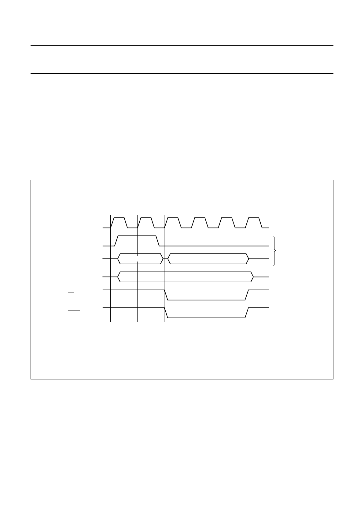
ALE
address/
data
address bus
RD
DMCS
The timing is configurable under firmware control.
Fig.3 Example of external data read (standard firmware).
address
internal
signals
external data
address
MHB462
1999 Jun 04 13
Philips Semiconductors Product specification
Global Positioning System (GPS)
baseband processor
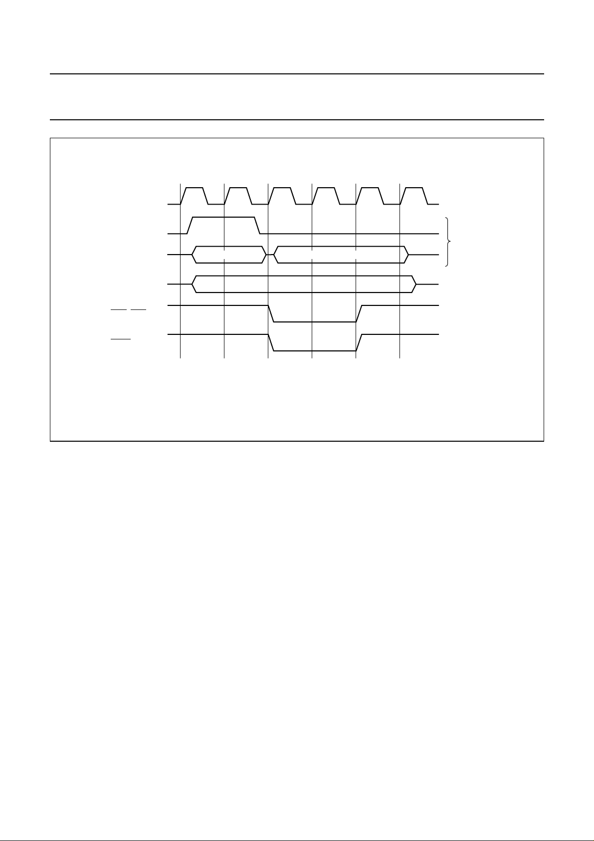
handbook, full pagewidth
XTAL1
ALE
address/
data
address bus
WRH/WRL
DMCS
address
SAA1575HL
internal
signals
external data
address
MHB463
The timing is configurable under firmware control.
Fig.4 Example of external data write (standard firmware).
7.4.2 CODE MEMORY SPACE The SAA1575HL has no internal code memory. The GPS
solution firmware resides in external memory. With the
standard Philips firmware, a ROM with a maximum access
time of 100 ns is required.
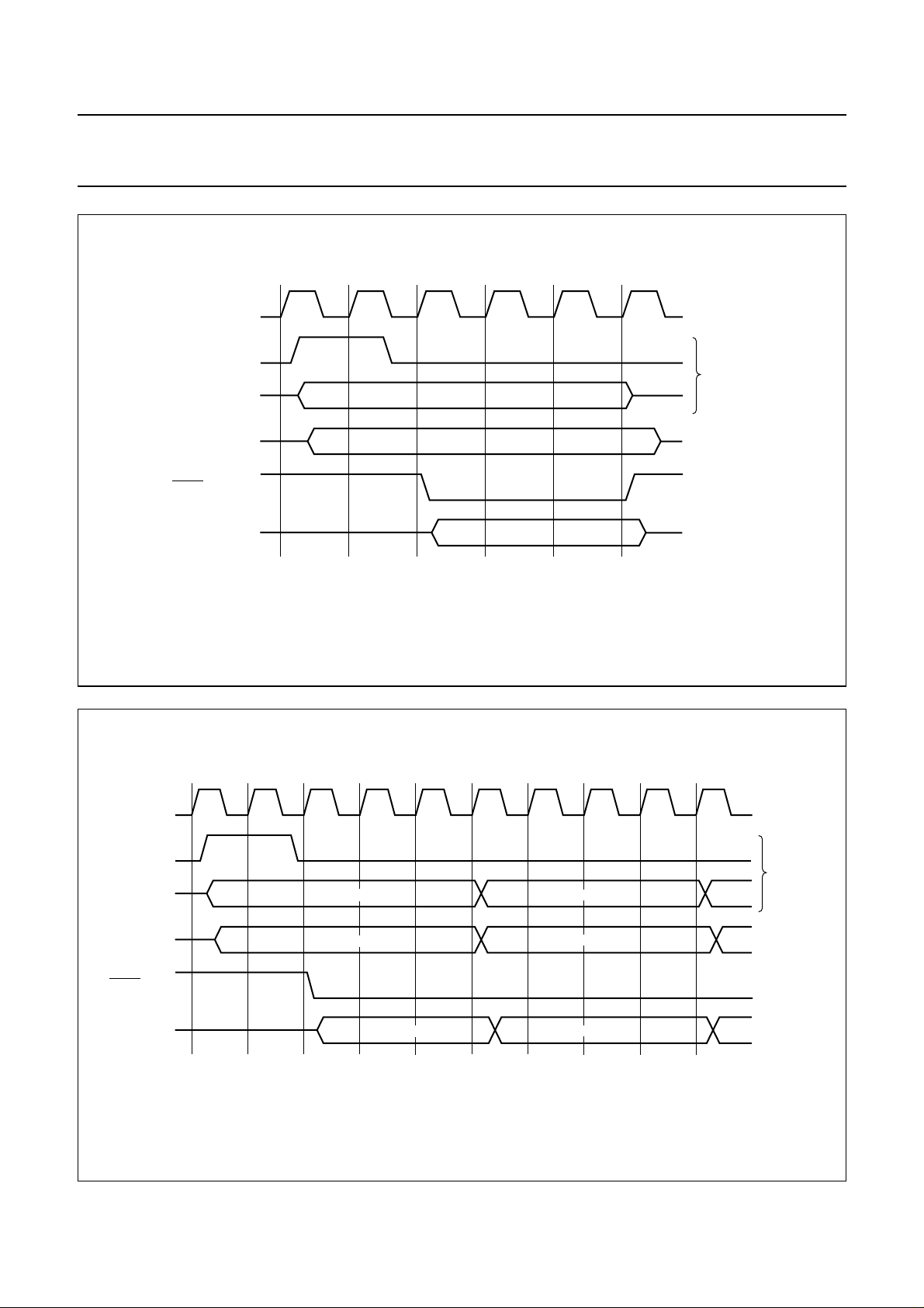
The classic operation of a multiplexed address/data bus
involves an address being set-up for every bus cycle.
The internal ALE signal is used to latch the address prior
to the cycle on which the data is set-up. An example of the
resulting timing is illustrated in Fig.5.
The SAA1575HL does not require an internal ALE cycle for
each code fetch. The lowest 3 address lines are not
multiplexed with the data lines and so these can be used
to incrementally read code locations.
The XA core can therefore issue up to 8 word reads
through sequential code memory for each ALE cycle. This
is termed a burst code read. An example of the resulting
timing is illustrated in Fig.6.
Any type of branch or jump in the program may require a
code fetch in a non-sequential manner and a new ALE
cycle will be needed. This may occur at any stage in a
code read. Thus the length of the read strobe in a burst
read is not necessarily an integer multiple of the individual
code read length.
1999 Jun 04 14
Philips Semiconductors Product specification
Global Positioning System (GPS)
baseband processor
handbook, full pagewidth
XTAL1
ALE
address/
data
address bus
PMCS
DATA BUS
SAA1575HL
internal
signals
address
address
data input
MHB464
The timing is configurable under firmware control.
Fig.5 Example of code read with ALE (standard firmware).
handbook, full pagewidth
XTAL1
ALE
address/
data
address
bus
PMCS
DATA BUS
address 1 address 2
address 1
code word 1
address 2
code word 2
internal
signals
MHB465
The timing is configurable under firmware control.
Fig.6 Example of burst mode code read (standard firmware).
1999 Jun 04 15

Philips Semiconductors Product specification
Global Positioning System (GPS)
baseband processor
7.5 CPU peripheral features
The SAA1575HL contains the hardware for 3 timers,
2 UARTs, a watchdog timer, a 3-bit RF IC programming
link and an 8-bit general purpose I/O port.
7.5.1 T
The SAA1575HL has 2 standard 16-bit timer/counters and
a third 16-bit up/down timer/counter. These timer/event
counters can perform the following functions:
• Measure time intervals and pulse duration
• Count external interrupts
• Generate interrupt requests
• Generate Pulse Width Modulation (PWM) or timed
output waveforms.
The timers are used by the standard Philips firmware to
generate the baud rates for the UART serial ports.
The additional features are not used in the standard
Philips firmware but are available for use in custom
firmware revisions.
All of the timers are configured in the 16-bit auto-reload
mode of operation. Timer 1 is used to generate the baud
rate for UART0 and Timer 2 is used to generate the baud
rate for UART1. In the standard Philips firmware, Timer 0
is not used.
7.5.2 W
The watchdog timer protects the system from incorrect
code execution by causing a processor reset if the
watchdog timer underflows as a result of a failure of the
firmware to feed the timer prior to it reaching its terminal
count.
In the standard Philips firmware, the watchdog is enabled
with a time-out period of 130 ms (at a clock frequency of
30 MHz).
IMERS/COUNTERS
ATCHDOG TIMER
SAA1575HL
With the standard Philips firmware, both UARTs are
configured to be in Mode 1: variable rate 8-bit operation.
Ten bits are transmitted (via TXDn) or received
(via RXDn): a START bit, 8 data bits (LSB first), and a
STOP bit.
In general, the UART clocks (which are 16 times the baud
rate) are determined by the Timer 1 or Timer 2 overflow
rate. With the standard Philips firmware, Timer 1 is used to
generate the baud rate for UART0 and Timer 2 is used to
generate the baud rate for UART1. The baud rate is set to
be 4800 bits/s for both UARTs.
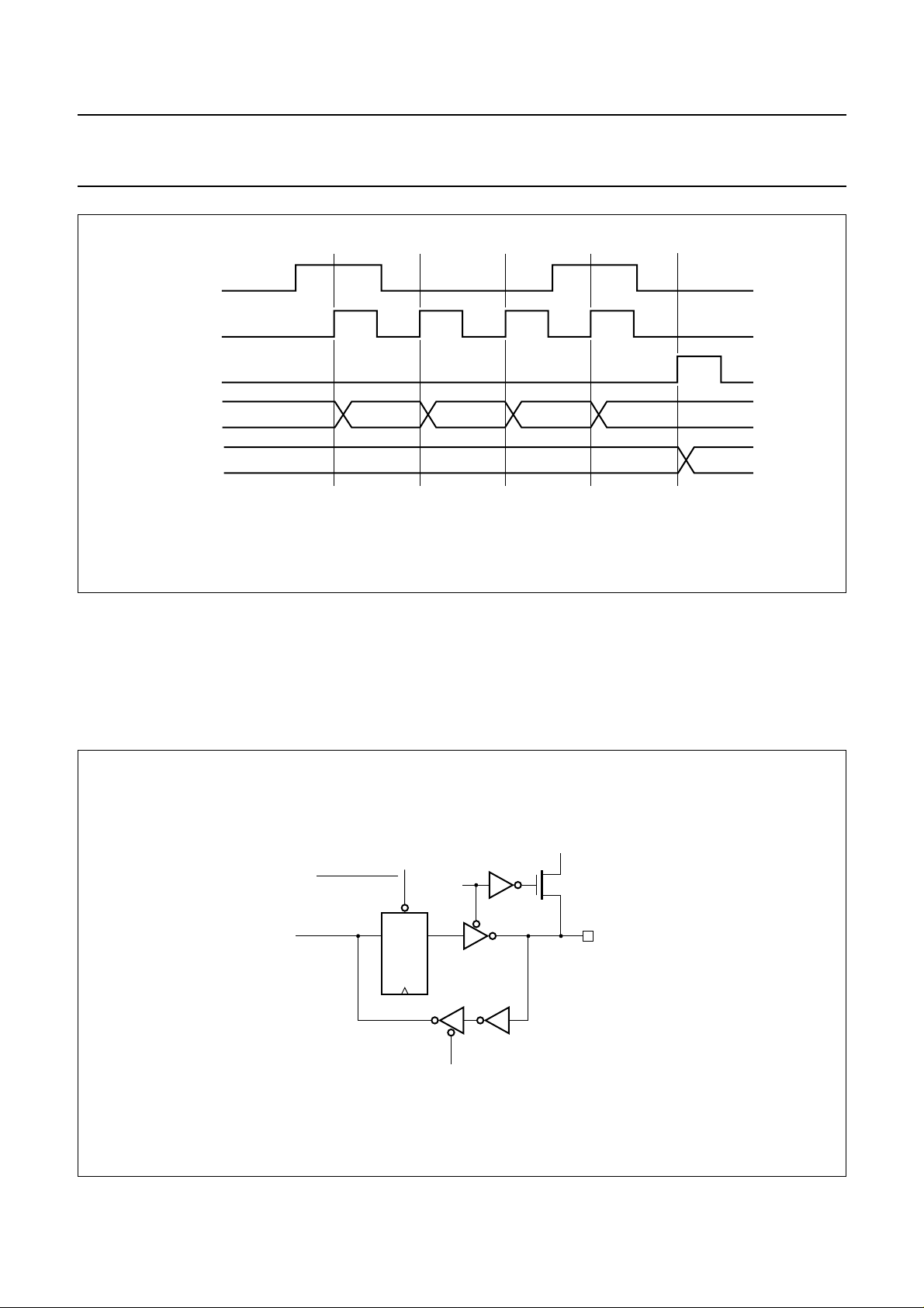
7.5.4 RF IC
The SAA1575HL is capable of programming the
UAA1570HL via a standard 3-wire serial link. This consists
of a clock line (SCLK), data line (D15 to D0) and a latch
enable (RFLE). Data is clocked into a holding register in
the UAA1570HL serially on each rising edge of the output
RFCLK. Once the complete serial packet has been
clocked into the RF IC, the latch enable output, RFLE, is
asserted which copies the new word from the holding
register in the RF IC into the control registers.
Proper timing of the clock, data and latch outputs is
ensured by firmware. An example sequence is illustrated
in Fig.7. The signals shown would result in the value 1001
being loaded into the last 4 bits of the RF IC serial register.
Each loading operation of the RF IC reloads the complete
RF control register.
With the standard Philips firmware, a 20-bit long word
0X5E320 is transmitted in this manner on start-up or
re-initialization. This gives full compatibility with the Philips
UAA1570HL front-end IC. See the
details about the configuration options of the front-end IC.
PROGRAMMING PORT
“UAA1570HL”
for more
7.5.3 UART
The SAA1575HL contains 2 UART ports, compatible with
the enhanced UART modes 1 to 3 on the 8xC51FB
(mode 0 operations not supported). With the exception of
the removal of the mode 0 operation, the UARTs in the
SAA1575HL are identical to those in the XA-G3 product.
Each UART rate is determined by either a fixed division of
the oscillator (in UART mode 2) or by one of the timer
overflow rates (in UART modes 1 and 3).
1999 Jun 04 16
S
Philips Semiconductors Product specification
Global Positioning System (GPS)
baseband processor
handbook, full pagewidth
RFDAT
RFCLK
RFLE
holding
control
X =don’t care.
Fig.7 Example timing for UAA1570HL programming.
XX10 1001XXX1 X100XXXX
XXXX
SAA1575HL
1001
MHB466
7.5.5 GENERAL PURPOSE I/O The SAA1575HL possesses an 8-bit general purpose I/O register and 8 associated I/Os (see Fig.8). With the standard
Philips firmware, all 8 of these pins are configured as outputs.
With the standard Philips firmware, only pin GPIO0 is used. This is switched on at the end of the firmware initialization
sequence and remains on subsequently.
pull-up
FET
V
CC(P)
MHB467
10 µA
GPIOn
pin
handbook, full pagewidth
WRITE ENABLE
DATA BUS
CFGn
EN
D
Q
IOn
CLK
READ ENABLE
Fig.8 GPIO pin drive circuits.
1999 Jun 04 17
 Loading...