

Philips SAA1310, SAA1310T Datasheet

INTEGRATED CIRCUITS
DATA SH EET
SAA1310
Control interface for VHS video
recorders
Product specification
File under Integrated Circuits, IC02
April 1995
Philips Semiconductors Product specification
Control interface for VHS video
SAA1310
recorders
FEATURES
• Full support of VISS and VASS mode (VHS
Index/Address Search System)
• Read, write and overwrite of Tape Control/head signal
(CTL)
• Power-ON and power-failure indicator
• 4 general purpose comparators for interface between
sensors and microprocessor
• 2 comparators have a 100 mA output driver
• PAL and NTSC compatible
ORDERING INFORMATION
EXTENDED
TYPE NUMBER
SAA1310 18 DIL plastic SOT102
SAA1310T 20 SO plastic SOT163A
PINS PIN POSITION MATERIAL CODE
GENERAL DESCRIPTION
The SAA1310 provides an interface between the tape
control head in the VHS deck-electronics.
The circuit also includes an interface between sensors in
the deck mechanics and the microprocessor.
PACKAGE
(1)
(2)
Note
1. SOT102-1; 1996 December 02.
2. SOT163-1; 1996 December 02.
April 1995 2
Philips Semiconductors Product specification
Control interface for VHS video recorders SAA1310
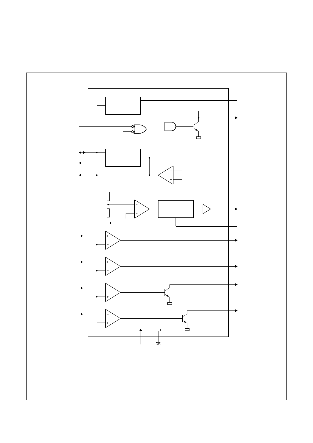
handbook, full pagewidth
write/read
input
control head data
output
capstan reverse
input
write
current
18
(20)
WRITE
AMPLIFIER
10
(11)
16
(18)
control head
input/output
control head
feedback
reference voltage
output
comparator 1
non - inverting input
comparator 2
non - inverting input
comparator 3
inverting input
(2)
(1)
(3)
(6)
(7)
(8)
2
1
3
5
6
7
AMPLIFIER
DETECTOR
V
P
FILTER
V
ref
comparator 1
comparator 2
comparator 3
V
ref
POWER-ON AND
POWER-FAILURE
DETECTOR
SAA1310
(SAA1310T)
17
(19)
(4)
15
(17)
14
(15)
13
(14)
4
power on/failure
output
power on/failure
capacitor
comparator 1
output
comparator 2
output
comparator 3
output
comparator 4
inverting input
Pin numbers in parenthesis refer to the SAA1310T.
8
(9)
comparator 4
9 (10)
P
12 (13)
Fig.1 Block diagram.
April 1995 3
11
(12)
MEA082 - 1
GNDV
comparator 4
output
Philips Semiconductors Product specification
Control interface for VHS video recorders SAA1310
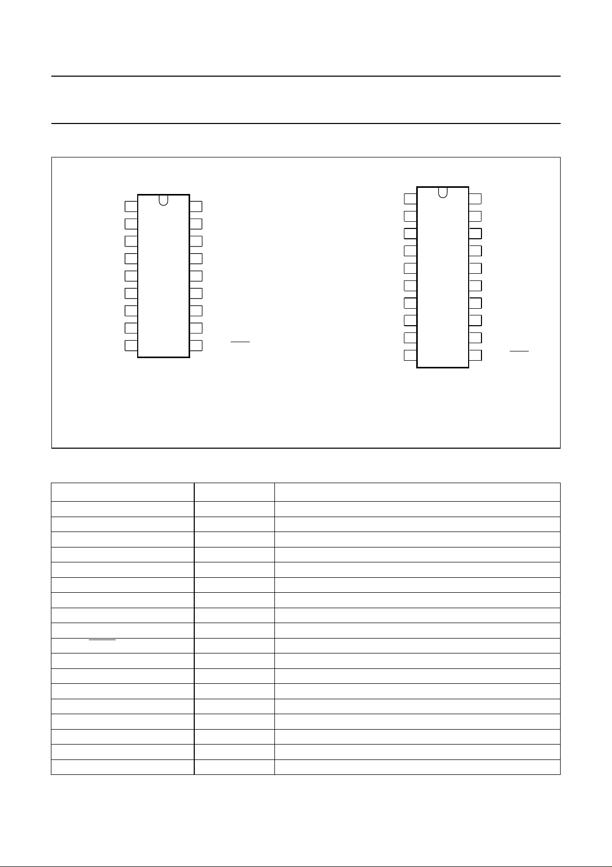
PIN CONFIGURATION
book, halfpage
CTL FB
CTL I/O
CPO/FAIL
V
ref
CIN1
CIN2
CIN3
CIN4
V
P
1
2
3
4
5
6
7
8
9
SAA1310
MEA083
18
CAPREV
17
PO/FAIL OUT
CTL DATA
16
15
COUT1
14
COUT2
13
COUT3
GND
12
11
COUT4
WRITE/READ
10
a. SAA1310.
Fig.2 Pin configurations.
PINNING (pins in parenthesis refer to SAA1310T)
handbook, halfpage
CPO/FAIL
CTL FB
CTL I/O
1
2
3
V
ref
4
n.c. n.c.
5
V
P
SAA1310T
6
7
8
9
10
MEA084
CIN1
CIN2
CIN3
CIN4
b. SAA1310T.
20
CAPREV
PO/FAIL OUT
19
CTL DATA
18
17
COUT1
16
COUT2
15
COUT3
14
GND
13
COUT4
12
WRITE/READ
11
SYMBOL PIN DESCRIPTION
CTL FB 1 (1) control head feedback
CTL I/O 2 (2) control head input/output
V
ref
3 (3) reference voltage output
CPO/FAIL 4 (4) power on/failure capacitor
CIN1 5 (6) comparator 1 input
CIN2 6 (7) comparator 2 input
CIN3 7 (8) comparator 3 input
CIN4 8 (9) comparator 4 input
V
P
WRITE/
READ 10 (11) write/read input
9 (10) supply voltage
COUT4 11 (12) comparator 4 output
GND 12 (13) ground
COUT3 13 (14) comparator 3 output
COUT2 14 (15) comparator 2 output
COUT1 15 (17) comparator 1 input
CTL DATA 16 (18) control head data output
PO/FAIL OUT 17 (19) power on/failure output
CAPREV 18 (20) capstan reverse input
April 1995 4
Philips Semiconductors Product specification
Control interface for VHS video recorders SAA1310
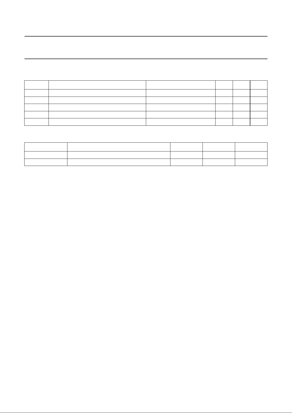
LIMITING VALUES (PIN NUMBERS IN PARENTHESIS REFER TO SAA1310T)
In accordance with the Absolute Maximum System (IEC 134)
SYMBOL PARAMETER CONDITIONS MIN. MAX. UNIT
V
P
V
I/VO
V
O
T
stg
T
amb
THERMAL RESISTANCE
R
th
R
th
supply voltage range 0 6.0 V
voltage on all pins except pins 11 (12) and 13 (14) 0 V
V
P
output voltage on pins 11 (12) and 13 (14) 0 18 V
storage temperature range −65 +150 °C
ambient temperature range 0 +70 °C
SYMBOL PARAMETER TYP. MAX. UNIT
thermal resistance (SAA1310) 75 − K/W
thermal resistance (SAA1310T) 90 − K/W
April 1995 5
 Loading...