

Philips SAA1101T, SAA1101P Datasheet

DATA SH EET
Product specification
File under Integrated Circuits, IC02
January 1990
INTEGRATED CIRCUITS
SAA1101
Universal sync generator (USG)
January 1990 2
Philips Semiconductors Product specification
Universal sync generator (USG) SAA1101
FEATURES
• Programmable to seven standards
• Additional outputs to simplify signal processing
• Can be synchronized to an external sync. signal
• Option to select the 524/624 line mode instead of the 525/625 line mode
• Lock from subcarrier to line frequency
GENERAL DESCRIPTION
The SAA1101 is a Universal Sync Generator (USG) and is designed for application in video sources such as cameras,
film scanners, video generators and associated apparatus. The circuit can be considered as a successor to the SAA1043
sync generator and the SAA1044 subcarrier coupling IC.
QUICK REFERENCE DATA
ORDERING AND PACKAGE INFORMATION
Notes
1. SOT117-1; 1996 December 02.
2. SOT136-1; 1996 December 02.
SYMBOL PARAMETER MIN. MAX. UNIT
V
DD
supply voltage range (pin 28) 4.5 5.5 V
I
DD
quiescent supply current − 10 µA
f
OSC
clock oscillator frequency − 24 MHz
EXTENDED
TYPE NUMBER
PACKAGE
PINS PIN POSITION MATERIAL CODE
SAA1101P 28 DIL plastic SOT117
(1)
SAA1101T 28 SO28 plastic SOT136A
(2)
January 1990 3
Philips Semiconductors Product specification
Universal sync generator (USG) SAA1101
, full pagewidth
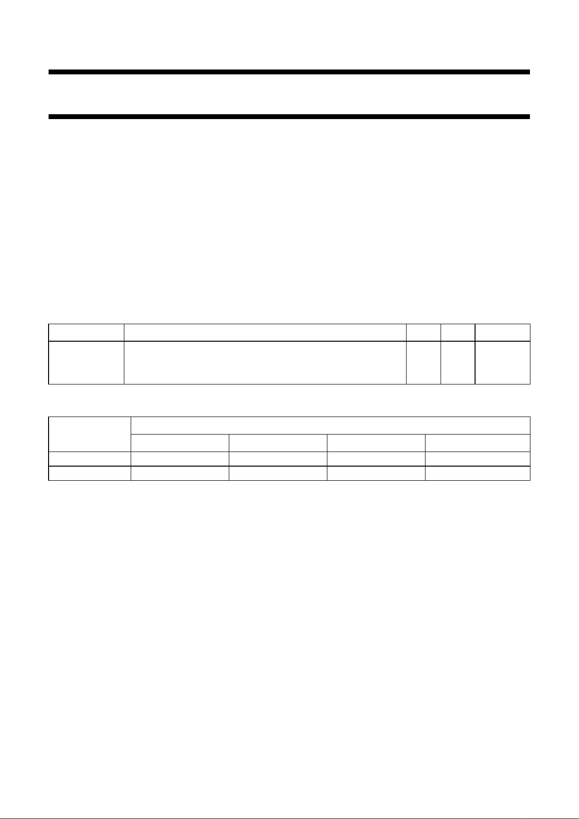
MGH191
COMBINING
LOGIC
VERTICAL
DIVIDER
RESET
PULSE
SHAPER
ADDITION/
SUPPRESSION
LOGIC
STANDARD
PROGRAMMED
DIVIDER
LINE
DIVIDER
HORIZONTAL
DETECTION
VERTICAL
DETECTION
VERTICAL
LOCK
SUBCARRIER
DIVIDER
SUBCARRIER
SUBTRACTION
LOCK MODE
SELECTION
PHASE
DETECTION
18171615222120
19
CSCBBKIDHDVDWMP
CLP12RR
7
VLE11ECS
f
s
− ∆f
f
s
∆f
f
H
H
ref
40f
H
HRI
f
H
2f
H
160f
H
PRESCALER
SAA1101
81428 910
PH LM1 LM0
NORM SI
13232434
CS1 CLOCS0
V
SS
V
DD
X
Y
Z
FSO
FSI
OSCO
OSCI
252627
2
1
6
5
Fig.1 Block diagram.
January 1990 4
Philips Semiconductors Product specification
Universal sync generator (USG) SAA1101
FUNCTIONAL DESCRIPTION
Generation of pulses
Generation of standard pulses such
as sync, blanking and burst for TV
systems: PAL B/G, PALN, PALM,
SECAM and NTSC. In addition a
number of non-standard pulses have
been supplied to simplify signal
processing. These signals include horizontal drive, vertical drive, clamp
pulse, identification etc. It is possible
to select the 524/624 line mode
instead of the 525/625 line mode for
all the above TV systems for
applications such as robotics, games
and computers.
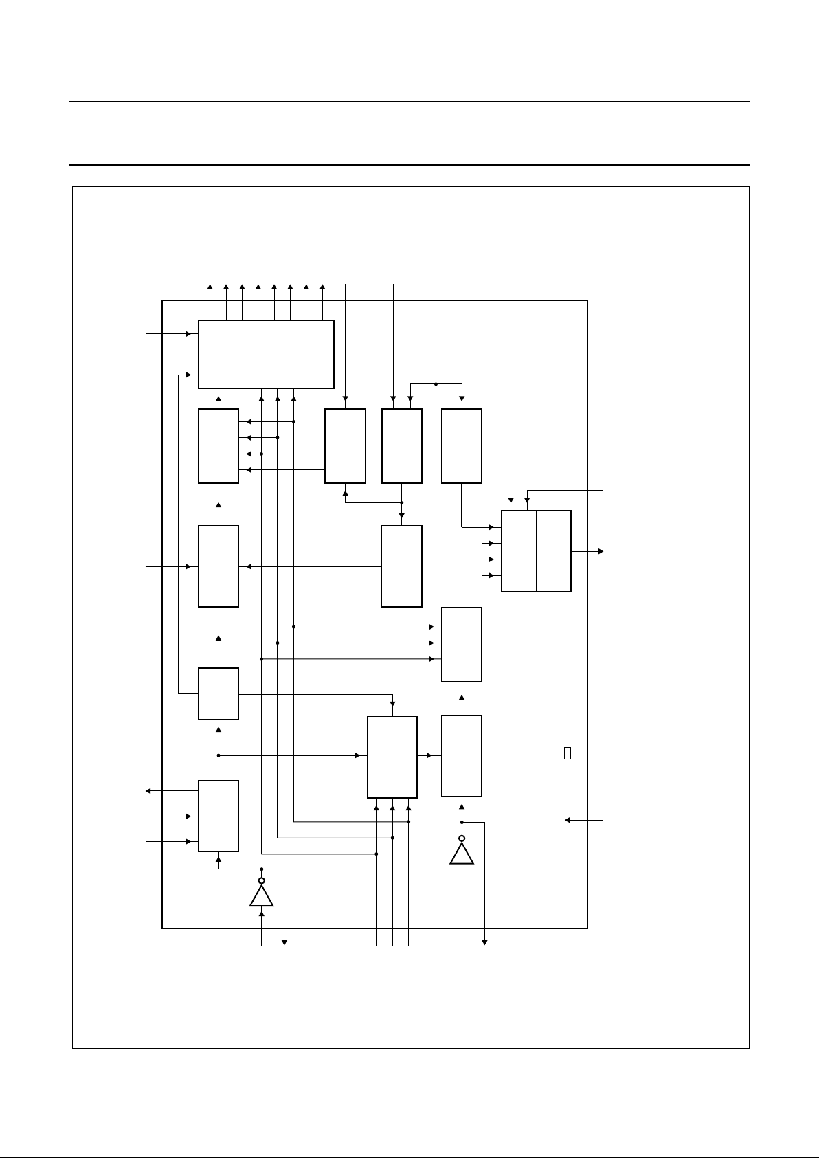
Fig.2 Pinning configuration;
SOT117.
page
FSI
FSO
CS1
CS0
OSCI
OSCO
VLE
PH
LM1
LM0
ECS
RR
SI
V
SS
V
DD
Z
Y
X
NORM
HD
CLO
VD
WMP
CLP
CS
CB
BK
ID
1
2
3
4
5
6
7
8
9
10
11
12
13
28
27
26
25
24
23
22
21
20
19
18
17
16
1514
SAA1101
MGH190
PINNING
SYMBOL PIN DESCRIPTION
FSI 1 subcarrier oscillator input, where f
max
= 5 MHz
FSO 2 subcarrier oscillator output
CS1 3 clock frequency selection - CMOS input
CS0 4 clock frequency selection - CMOS input
OSCI 5 clock oscillator input, where f
max
= 24 MHz
OSCO 6 clock oscillator output
VLE 7 vertical in-lock enable - CMOS input
PH 8 phase detector output - 3-state output
LM1 9 lock mode selection - CMOS input
LM0 10 lock mode selection - CMOS input
ECS 11 external composite sync. signal - CMOS Schmitt-trigger
input
RR 12 frame reset - CMOS Schmitt-trigger input
SI 13 set identification, used to set the correct field sequence in
P AL-mode. The correction (inversion of fH2) is done at the
left-hand slope of the SI-pulse. Minimum pulse width is
800 ns. CMOS Schmitt-trigger input.
V
SS
14 ground
ID 15 identification - push-pull output
BK 16 burst key (PAL/NTSC), chroma-blanking (SECAM) -
push-pull output
CB 17 composite blanking - push-pull output
CS 18 composite sync. - push-pull output
CLP 19 clamp pulse - push-pull output
WMP 20 white measurement pulse-3-state output
VD 21 vertical drive pulse - push-pull output
HD 22 horizontal drive pulse - push-pull output
NORM 23 used with X, Y and Z to select TV system; NORM = 0,
625/525 line mode (standard);
NORM = 1, 624/524 line mode - CMOS input
CLO 24 clock output - push-pull output
X 25 TV system selection input - CMOS input
Y 26 TV system selection input - CMOS input
Z 27 TV system selection input - CMOS input
V
DD
28 voltage supply
January 1990 5
Philips Semiconductors Product specification
Universal sync generator (USG) SAA1101
Lock modes
The USG offers four lock modes:
• Lock from the subcarrier
• Slow sync. lock, external H
ref
• Slow sync. lock, internal H
ref
• Fast sync. lock, internal H
ref
LOCK FROM SUBCARRIER
Lock from subcarrier to the line frequency for the above
mentioned TV systems is given below; the horizontal
frequency (fH) = 15.625 kHz for 625 line systems and
15.734264 kHz for 525 line systems.
These relationships are obtained by the use of a phase
locked loop and the internal programmed divider chain,
see Fig.3(a).
LOCK TO AN EXTERNAL SIGNAL SOURCE
The following methods can be used to lock to an external
signal source:
1. Sync. lock slow; the line frequency is locked to an
external signal. The line and frame information are
extracted from the external sync. signal and used
separately in the lock system. The line information is
used in a phase-locked loop where external and
internal line frequencies are compared by the same
phase detector as is used for the subcarrier lock. The
external frame information is compared with the
internal frame in a slow lock system; mismatch of
internal and external frames will result in the addition
or suppression of one line depending on the direction
of the fault. The maximum lock time for frame lock is
6.25 s, see Fig.3(b).
2. Sync. lock fast. A fast lock of frames is possible with a
frame reset which is extracted out of the incoming
external sync. signal, see Fig.3(c).
3. Sync. lock with external reference. Lock of an external
sync. signal to the line frequency with an external line
reference to make possible a shifted lock. The
SECAM (1 and 2) 282f
H
PALN 229.2516f
H
NTSC (1 and 2) 227.5f
H
PALM 227.25f
H
PAL B/G 283.7516f
H
subcarrier input is, in this case, used as an external
input for the horizontal reference, see Fig.3(d).
SELECTION OF LOCK MODE
Lock mode is selected using the inputs LM0 and LM1 as
illustrated in the Table below.
LM0 LM1 SELECTION
0 0 lock to subcarrier
0 1 slow sync. lock external H
ref
1 0 slow sync. lock internal H
ref
1 1 fast sync. lock internal H
ref
January 1990 6
Philips Semiconductors Product specification
Universal sync generator (USG) SAA1101
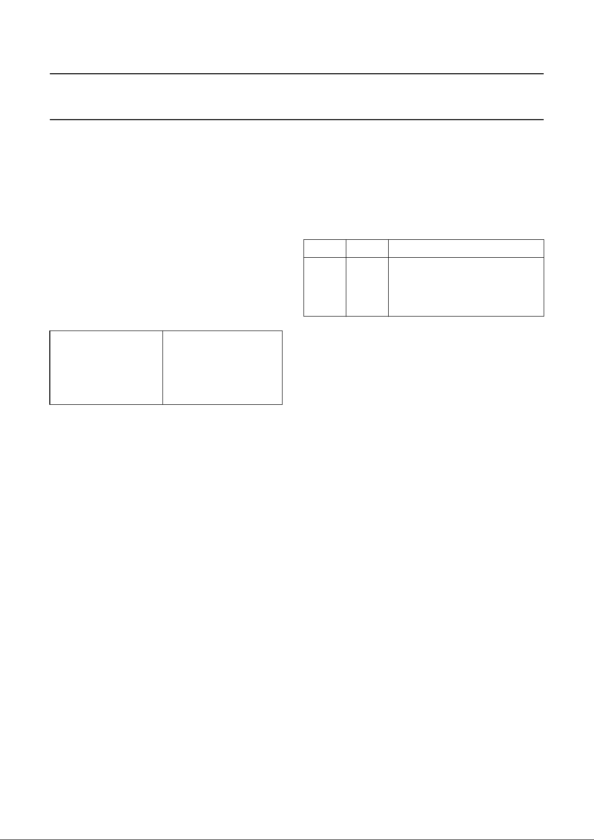
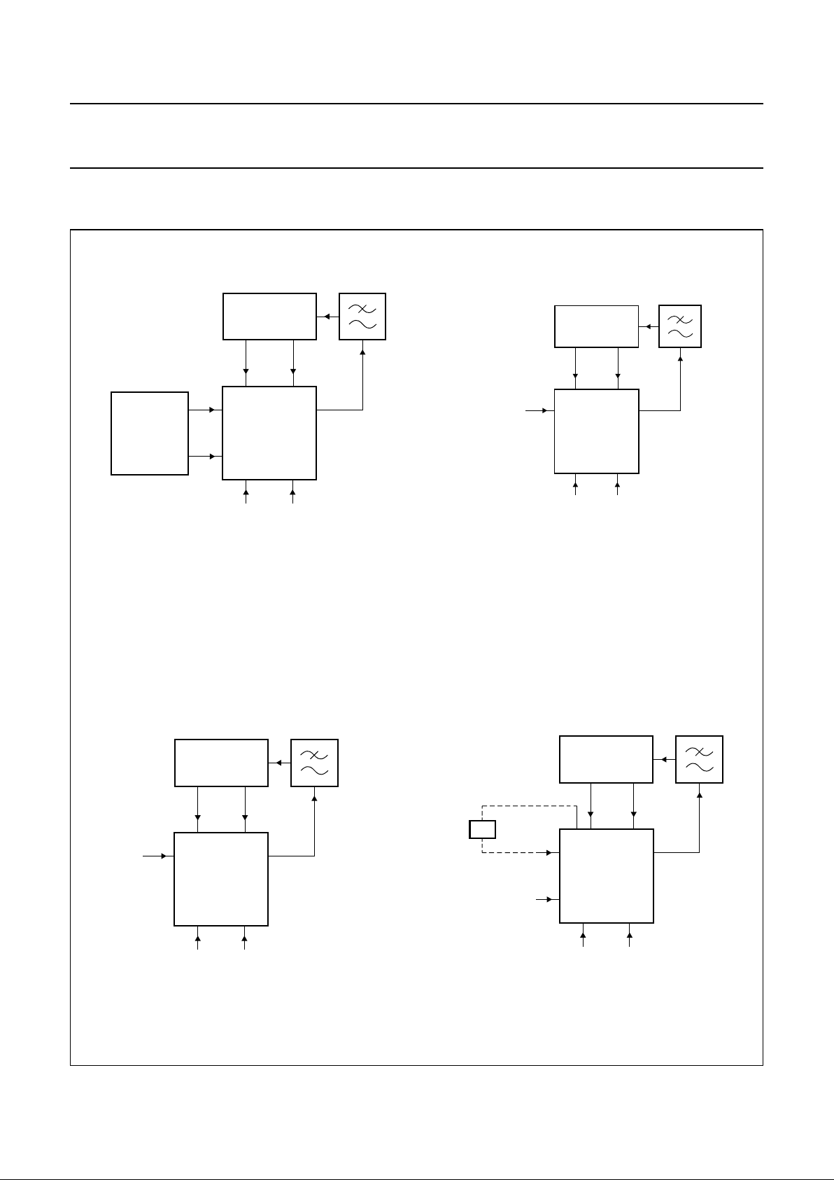
The different lock modes are illustrated by the following figures:
Fig.3 (a) Lock to subcarrier.
Fig.3 (b) Slow sync lock, internal H
ref
Fig.3 (c) Fast sync lock, internal H
ref
Fig.3 (d) Slow sync lock, external H
ref
handbook, halfpage
MGH193
n × f
H
LINE
OSCILLATOR
FSO
FSI
OSCO OSCI
SAA1101
SUB-
CARRIER
OSCILLATOR
PH
LM1LM0
logic 0 logic 1
10
65
8
2
1
9
handbook, halfpage
MGH194
n × f
H
LINE
OSCILLATOR
ECS
OSCO OSCI
SAA1101
PH
LM1LM0
logic 0 logic 1
10
65
8
11
9
handbook, halfpage
MGH195
n × f
H
LINE
OSCILLATOR
ECS
OSCO OSCI
SAA1101
PH
LM1LM0
logic 1 logic 1
10
65
8
11
9
handbook, halfpage
MGH192
n × f
H
LINE
OSCILLATOR
τ
H
ref
ECS
FSI
H
D OSCO OSCI
SAA1101
PH
LM1LM0
logic 0 logic 1
10
65
8
22
11
1
9
 Loading...