

Philips SAA1064, SAA1064T Datasheet

INTEGRATED CIRCUITS
DATA SH EET
SAA1064
4-digit LED-driver with I
interface
Product specification
File under Integrated Circuits, IC01
2
C-Bus
February 1991
Philips Semiconductors Product specification
4-digit LED-driver with I2C-Bus interface
GENERAL DESCRIPTION
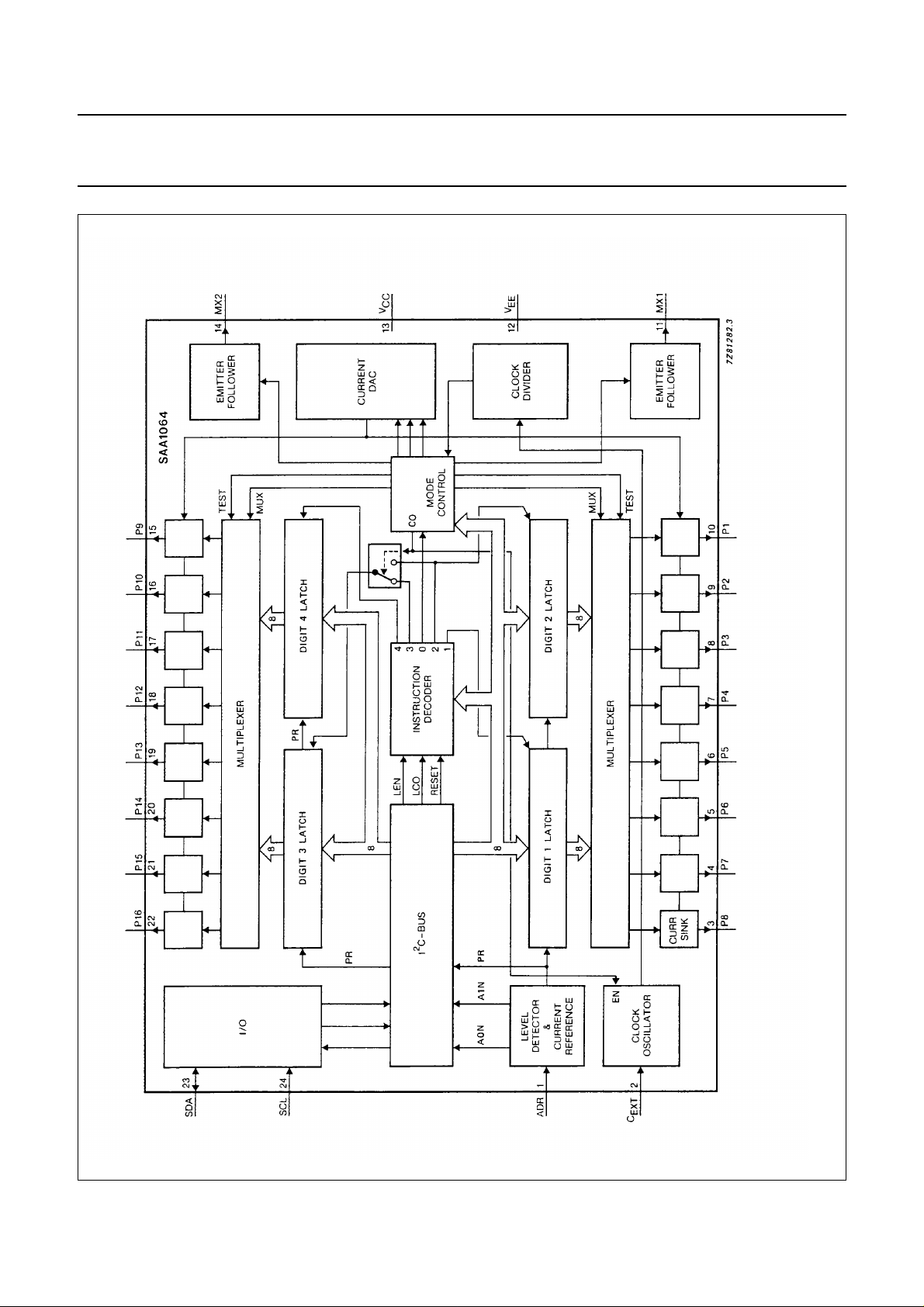
The LED-driver is a bipolar integrated circuit made in an
I2L compatible 18 volts process. The circuit is especially
designed to drive four 7-segment LED displays with
decimal point by means of multiplexing between two pairs
of digits. It features an I2C-Bus slave transceiver interface
with the possibility to program four different SLAVE
ADDRESSES, a POWER RESET flag, 16 current sink
OUTPUTS, controllable by software up to 21 mA, two
multiplex drive outputs for common anode segments, an
on-chip multiplex oscillator, control bits to select static,
dynamic and blank mode, and one bit for segment test.
QUICK REFERENCE DATA
PARAMETER CONDITIONS SYMBOL MIN. TYP. MAX. UNIT
Supply voltage V
Supply current all outputs OFF V
Total power dissipation
24-lead DIL (SOT101B) P
24-lead DIL SO (SOT137A) P
Operating ambient
temperature range T
= 0 V V
EE
= 5 V I
CC
CC
CC
tot
tot
amb
(1)
SAA1064
4.5 5 15 V
7 9.5 14 mA
−−1000 mW
−−500 mW
−40 − +85 °C
Note
1. The positive current is defined as the conventional current flow into a device (sink current).
PACKAGE OUTLINE
SAA1064: 24-lead DIL; plastic with internal heat spreader (SOT101B); SOT101-1; 1996 August 30.
SAA1064T: 24-lead mini-pack; plastic (SO-24; SOT137A); SOT137-1; 1996 August 30.
February 1991 2
Philips Semiconductors Product specification
4-digit LED-driver with I2C-Bus interface
SAA1064
February 1991 3
Fig.1 Block diagram.
Philips Semiconductors Product specification
4-digit LED-driver with I2C-Bus interface
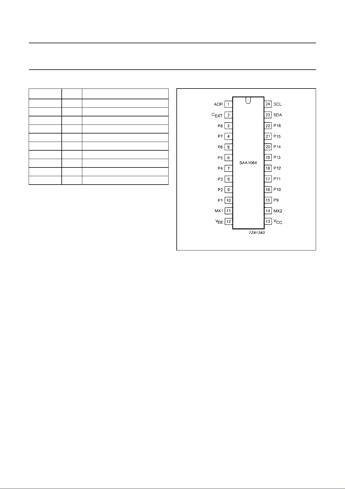
PINNING
SYMBOL PIN DESCRIPTION
2
ADR 1 I
C
EXT
2 external control
P8 to P1 3-10 segment output
MX1 11 multiplex output
V
EE
V
CC
12 ground
13 positive supply
MX2 14 multiplex output
P9 to P16 15-22 segment output
SDA 23 I
SCL 24 I
C-Bus slave address input
2
C-Bus serial data line
2
C-Bus serial clock line
SAA1064
Fig.2 Pinning diagram.
February 1991 4
Philips Semiconductors Product specification
4-digit LED-driver with I2C-Bus interface
FUNCTIONAL DESCRIPTION
a. READ mode.
SAA1064
b. WRITE mode.
S = start condition A1, A0 = programmable address bits
P = stop condition SC SB SA = subaddress bits
A = acknowledge C6 to C0 = control bits
X = don’t care PR = POWER RESET flag
Fig.3 I2C-Bus format.
Address pin ADR
Four different slave addresses can be chosen by connecting ADR either to V
the corresponding valid addresses HEX 70, 72, 74 and 76 for writing and 71, 73, 75 and 77 for reading. All other
addresses cannot be acknowledged by the circuit.
3/8 VCC, 5/8 VCCor VCC. This results in
EE,
February 1991 5

Philips Semiconductors Product specification
4-digit LED-driver with I2C-Bus interface
Status byte
Only one bit is present in the status byte, the POWER RESET flag. A logic 1 indicates the occurence of a power failure
since the last time it was read out. After completion of the READ action this flag will be set to logic 0.
Subaddressing
The bits SC, SB and SA form a pointer and determine to which register the data byte following the instruction byte will
be written. All other bytes will then be stored in the registers with consecutive subaddresses. This feature is called
Auto-Increment (AI) of the subaddress and enables a quick initialization by the master.
The subaddress pointer will wrap around from 7 to 0.
The subaddresses are given as follows:
SC SB SA SUB-ADDRESS FUNCTION
0 0 0 00 control register
0 0 1 01 digit 1
0 1 0 02 digit 2
0 1 1 03 digit 3
1 0 0 04 digit 4
1 0 1 05 reserved, not used
1 1 0 06 reserved, not used
1 1 1 07 reserved, not used
SAA1064
Control bits (see Fig.4)
The control bits C0 to C6 have the following meaning:
C0 = 0 static mode, i.e. continuous display of digits 1 and 2
C0 = 1 dynamic mode, i.e. alternating display of digit 1 + 3 and 2 + 4
C1 = 0/1 digits 1 + 3 are blanked/not blanked
C2 = 0/1 digits 2 + 4 are blanked/not blanked
C3 = 1 all segment outputs are switched-on for segment test
C4 = 1 adds 3 mA to segment output current
C5 = 1 adds 6 mA to segment output current
C6 = 1 adds 12 mA to segment output current
Note
1. At a current determined by C4, C5 and C6.
Data
A segment is switched ON if the corresponding data bit is logic 1. Data bits D17 to D10 correspond with digit 1, D27 to
D20 with digit 2, D37 to D30 with digit 3 and D47 to D40 with digit 4.
The MSBs correspond with the outputs P8 and P16, the LSBs with P1 and P9. Digit numbers 1 to 4 are equal to their
subaddresses (hex) 1 to 4.
(1)
February 1991 6
 Loading...