Philips SAA1057 Datasheet

INTEGRATED CIRCUITS
DATA SH EET
SAA1057
Radio tuning PLL frequency
synthesizer
Product specification
File under Integrated Circuits, IC01
November 1983

Philips Semiconductors Product specification
Radio tuning PLL frequency synthesizer SAA1057
GENERAL DESCRIPTION
The SAA1057 is a single chip frequency synthesizer IC in
I2L technology, which performs all the tuning functions of a
PLL radio tuning system. The IC is applicable to all types
of radio receivers, e.g. car radios, hi-fi radios and portable
radios.
• On-chip programmable current amplifier (charge pump)
to adjust the loop gain.
• Only one reference frequency for both AM and FM.
• High signal purity due to a sample and hold phase
detector for the in-lock condition.
• High tuning speed due to a powerful digital memory
phase detector during the out-lock condition.
Features
• On-chip prescaler with up to 120 MHz input frequency.
• On-chip AM and FM input amplifiers with high sensitivity
(30 mV and 10 mV respectively).
• Low current drain (typically 16 mA for AM and 20 mA for
FM) over a wide supply voltage range (3,6 V to 12 V).
• Tuning steps for AM are: 1 kHz or 1,25 kHz for a VCO
frequency range of 512 kHz to 32 MHz.
• Tuning steps for FM are: 10 kHz or 12,5 kHz for a VCO
frequency range of 70 MHz to 120 MHz.
• Serial 3-line bus interface to a microcomputer.
• Test/features.
• On-chip amplifier for loop filter for both AM and FM (up
to 30 V tuning voltage).
QUICK REFERENCE DATA
Supply voltage ranges V
Supply currents I
Input frequency ranges
at pin FAM f
at pin FFM f
Maximum crystal input frequency f
Operating ambient temperature range T
CC1
V
CC2
V
CC3
CC1
I
CC3
FAM
FFM
XTAL
amb
+ I
CC2
3,6 to 12 V
3,6 to 12 V
V
to 31 V
CC2
typ. 18 mA
typ. 0,8 mA
512 kHz to 32 MHz
70 to 120 MHz
> 4 MHz
−25 to + 80 °C
PACKAGE OUTLINE
18-lead DIL; plastic (SOT102H); SOT102-1; 1996 September 2.
November 1983 2

Philips Semiconductors Product specification
Radio tuning PLL frequency synthesizer SAA1057
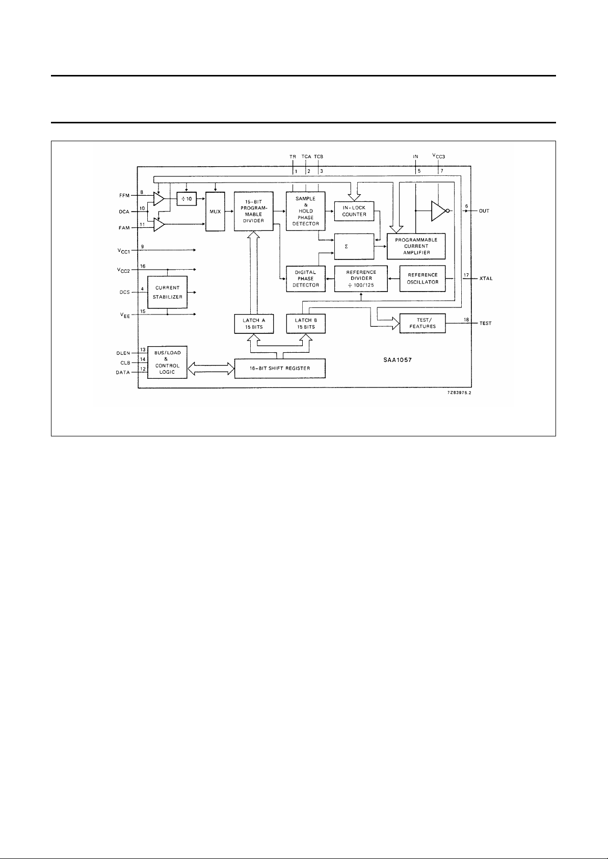
Fig.1 Block diagram.
GENERAL DESCRIPTION
The SAA1057 performs the entire PLL synthesizer
function (from frequency inputs to tuning voltage output)
for all types of radios with the AM and FM frequency
ranges.
The circuit comprises the following:
• Separate input amplifiers for the AM and FM
VCO-signals.
• A divider-by-10 for the FM channel.
• A multiplexer which selects the AM or FM input.
• A 15-bit programmable divider for selecting the required
frequency.
• A sample and hold phase detector for the in-lock
condition, to achieve the high spectral purity of the VCO
signal.
• A digital memory frequency/phase detector, which
operates at a 32 times higher frequency than the sample
and hold phase detector, so fast tuning can be achieved.
• An in-lock counter detects when the system is in-lock.
The digital phase detector is switched-off automatically
when an in-lock condition is detected.
• A reference frequency oscillator followed by a reference
divider. The frequency is generated by a 4 MHz quartz
crystal. The reference frequency can be chosen either
32 kHz or 40 kHz for the digital phase detector (that
means 1 kHz and 1,25 kHz for the sample and hold
phase detector), which results in tuning steps of 1 kHz
and 1,25 kHz for AM, and 10 kHz and 12,5 kHz for FM.
• A programmable current amplifier (charge pump), which
controls the output current of both the digital and the
sample/hold phase detector in a range of 40 dB. It also
allows the loop gain of the tuning system to be adjusted
by the microcomputer.
• A tuning voltage amplifier, which can deliver a tuning
voltage of up to 30 V.
• BUS; this circuitry consists of a format control part, a
16-bit shift register and two 15-bit latches. Latch A
contains the to be tuned frequency information in a
binary code. This binary-coded number, multiplied by
the tuning spacing, is equal to the synthesized
frequency. The programmable divider (without the fixed
divide-by-10 prescaler for FM) can be programmed in a
range between 512 and 32 767 (see Fig.3). Latch B
contains the control information.
November 1983 3

Philips Semiconductors Product specification
Radio tuning PLL frequency synthesizer SAA1057
OPERATION DESCRIPTION
Control information
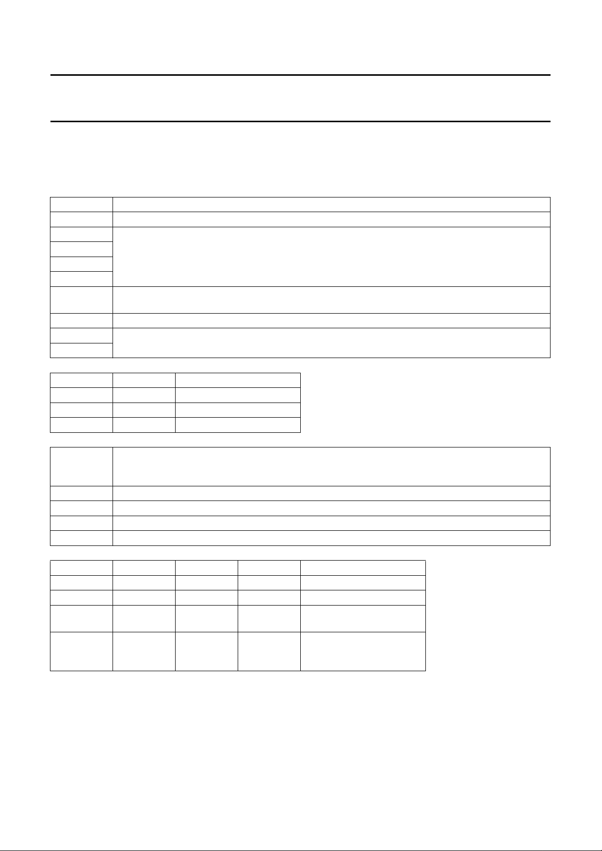
The following functions can be controlled with the data word bits in latch B. For data word format and bit position see
Fig.3.
FM FM/AM selection; ‘1’ = FM, ‘0’ = AM
REFH reference frequency selection; ‘1’ = 1,25 kHz, ‘0’ = 1 kHz (sample and hold phase detector)
CP3
CP2
CP1
CP0
SB2 enables last 8 bits (SLA to T0) of data word B; ‘1’ = enables, ‘0’ = disables; when programmed ‘0’, the
SLA load mode of latch A; ‘1’ = synchronous, ‘0’ = asynchronous
PDM1
PDM0
control bits for the programmable current amplifier (see section Characteristics)
last 8 bits of data word B will be set to ‘0’ automatically
phase detector mode
PDM1 PDM0 digital phase detector
0 X automatic on/off
10 on
1 1 off
BRM bus receiver mode bit; in this mode the supply current of the BUS receiver will be switched-off
automatically after a data transmission (current-draw is reduced); ‘1’ = current switched; ‘0’ = current
always on
T3 test bit; must be programmed always ‘0’
T2 test bit; selects the reference frequency (32 or 40 kHz) to the TEST pin
T1 test bit; must be programmed always ‘0’
T0 test bit; selects the output of the programmable counter to the TEST pin
T3 T2 T1 T0 TEST (pin 18)
00001
0 1 0 0 reference frequency
0 0 0 1 output programmable
counter
0 1 0 1 output in-lock counter
‘0’ = out-lock
‘1’ = in-lock
November 1983 4
 Loading...