

Philips SA9504 Datasheet
INTEGRATED CIRCUITS
SA9504
Dual-band, PCS(CDMA)/AMPS
LNA and downconverter mixers
Preliminary specification
Supersedes data of 1999 Aug 24
1999 Oct 28
Philips Semiconductors Preliminary specification
Dual-band, PCS(CDMA)/AMPS
LNA and downconverter mixers
DESCRIPTION
The SA9504 is an integrated receiver front-end for 900 MHz Cellular
(AMPS) and 1.9 GHz PCS (CDMA) phones. This dual-band receiver
circuit has low noise amplifiers and downconverters for both bands,
and provides an elegant solution for RF-to-IF conversion.
The two cascode LNAs have been designed to provide high gain
with very low noise figures and high linearity. The downconverter
portion is based on the Philips SA9502. There are two individual
mixer blocks, each optimized for low noise figure and high linearity.
The whole circuit is designed for low power consumption, high
performance, and is compatible with the requirements for Cellular
(AMPS) and PCS (CDMA) handsets.
The circuit has been designed in our advanced QUBiC3 BiCMOS
process with 30 GHz f
FEATURES
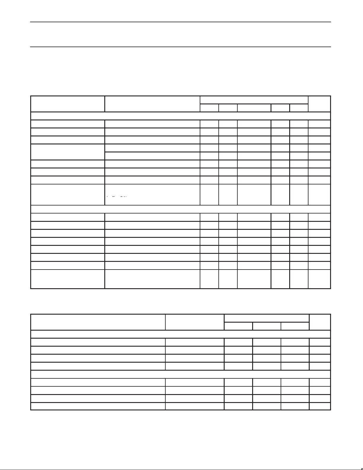
LNA typical performance
PARAMETER Cellular LNA PCS (CDMA) LNA
Gain (dB) 16.5 14.8
Noise figure (dB) 1.6 2
Input IP3 (dBm) –2 1
Current (mA) 4.9 4.9
•LNAs for both Cellular (AMPS) and PCS (CDMA) bands
•High gain, low noise figure, high linearity performance
•Cascode output structure requiring no external matching
•Low power consumption, typical 4.9 mA
•Low voltage operation down to 2.7 volts
and 60 GHz f
T
MAX
.
SA9504
Downconverter typical performance
PARAMETER Cellular FM PCS (CDMA)
Gain (dB) 7.5 11.5
Nois e Figure ( dB) 10 9
Input IP3 (dBm) 5 4
Current (mA)
(Tx) LO output buffer off
•Separate, selectable IF outputs to suit FM and CDMA bandwidths
•Buffered Cellular and PCS LO inputs
•Integrated frequency doubler for PCS mixer LO
•Differential (Tx) LO output buffer (can be switched on or off)
•Low voltage operation down to 2.7 volts
•Mixers current consumption with (Tx) LO buffer on:
– Cellular FM: 17.4 mA
– PCS: 27.6 mA
•Low standby current in sleep mode: <50 µA
•Small LQFP32 package
APPLICATIONS
•800 MHz analog FM and receivers
•1.9 GHz PCS (CDMA) digital receivers
•Supports dual-band operation
•Digital mobile communications equipment
•Portable, low power radio equipment
6.9 17
1999 Oct 28
2
Philips Semiconductors Preliminary specification
PARAMETER
TEST CONDITIONS
UNIT
Dual-band, PCS(CDMA)/AMPS
LNA and downconverter mixers
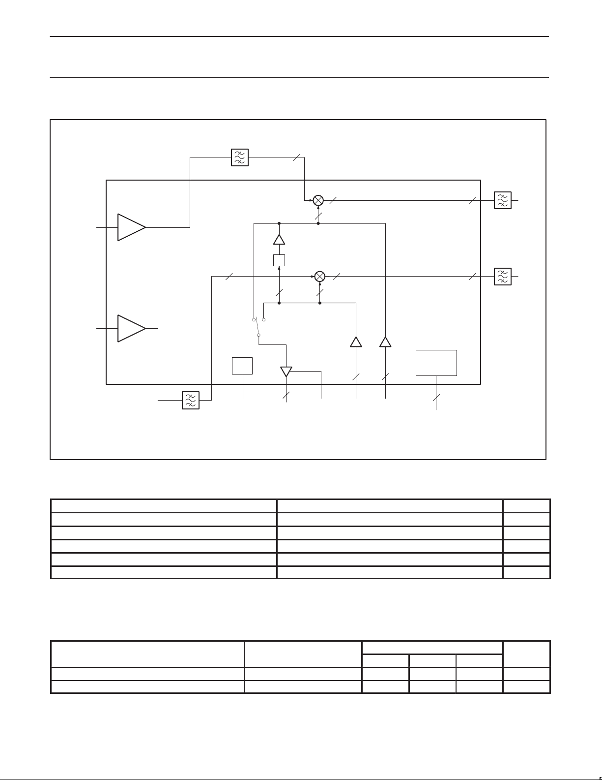
BLOCK DIAGRAM
RF_PCS
SA9504
RF_CEL
RX BPF
Fo = 1960 MHz
BW = 60 MHz
PCS_INPCS_OUT
SA9504
2
PCS IF BPF
2
2
×2
2
2
CELLULARPCS
2
PCS_IF
FM_IF
2
21
BW = 1.23MHz
FM IF BPF
BW = 30kHz
MODE
SELECT
LOGIC
4
LO_X2_EN
PCS/CELLULAR
S0
S1
SR02107
CEL_OUT
CEL_IN
RX BPF
Fo = 881.5MHz
BW = 25 MHz
BIAS
CTRL
V
CC
2
LO_OUT
1
LO_ENABLE CEL
LO_IN
1
PCS
LO_IN
Figure 1. SA9504 Block Diagram
ABSOLUTE MAXIMUM RATINGS
PARAMETER
1
RATINGS UNIT
Supply voltage (VCC) –0.3 to +3.6 V
Logic input voltage –0.3 to VCC+0.3 V
Maximum power input +20 dBm
Power dissipation (T
= 25°C) 800 mW
amb
Storage temperature range –65 to +150 °C
NOTES:
1. Stresses beyond those listed may cause permanent damage to the device. These are stress ratings only and functional operation of the
device at these or any other conditions beyond those indicated under “Recommended Operating Conditions” is not implied. Exposure to
absolute-maximum-rated-conditions for extended periods may affect device reliability.
RECOMMENDED OPERATING CONDITIONS
LIMITS
MIN TYP MAX
Supply voltage (VCC) 2.7 2.85 3.3 V
Operating ambient temperature range (T
) –40 +85 °C
amb
1999 Oct 28
3

Philips Semiconductors Preliminary specification
Dual-band, PCS(CDMA)/AMPS
LNA and downconverter mixers
FUNCTIONAL DESCRIPTION
Mode selection
The SA9504 has several modes of operation for which the selection
logic is defined in Table 1. Different mode selections require different
portions of the circuit to be active. Modes from unlisted combinations
of logic pins are not permitted. The LNA and downconverter together
can be programmed to operate in the PCS or cellular bands using
the PCS/CEL logic input pin.
In order for the SA9504 to function correctly, a reset must be applied
on first power-up. The whole circuit (LNAs and mixers) is powered
down when control lines S0 and S1 are simultaneously held HIGH.
An internal reset is applied upon releasing the circuit from
power-down (on taking S0 = S1 from HIGH to LOW).
LNA
The SA9504 has two LNAs, one for cellular FM, and one for PCS
(CDMA). The LNAs have been designed for high gain, low noise
figure and good linearity with low power consumption. External
components can be used to match the LNA inputs for the Cellular
and PCS bands. The LNAs employ a cascode output structure
allowing high gain and excellent reverse isolation. The LNA outputs
are internally matched to drive 50Ω external loads. The input and
output return loss of better than 10 dB can be achieved in all modes.
Downconverter
The SA9504 has two mixers, one for Cellular FM, and one for PCS
(CDMA). Each mixer is individually optimized for its specific
SA9504
requirements. The Cellular FM mixer has a common single-ended
RF input. The PCS mixer’s RF input port is differential, and requires
an external balun when used with a single-ended source. Both the
PCS and the Cellular mixer RF inputs should be AC coupled.
Local oscillator drive for the mixers is provided through pins
CEL LO_IN and/or PCS LO_IN. The local oscillator inputs are
single-ended, AC-coupled. The CEL LO_IN signal is internally
buffered to drive the following:
– (Tx) LO output buf fer,
– cellular FM mixer,
– PCS LO frequency doubler.
In the PCS mode, mixer LO drive can be either direct (PCS LO_IN)
or through the frequency doubler after CEL LO_IN. The mixer local
oscillator signal is made available externally via the (Tx) LO output
buffer for potential use elsewhere in the radio. For example, this
signal typically can be used with the transmitter circuitry. The
(Tx) LO output buffer can be powered down independently, using
the (Tx) LO_ENABLE logic input. The (Tx) LO output buffer has
open collector differential outputs which should be externally biased
to power supply rail.
The PCS and Cellular FM mixers have open collector differential IF
outputs. The differential IF outputs must be biased at the supply
voltage through external inductors that may also be part of the
matching circuit to the SAW filter .
1999 Oct 28
4
Philips Semiconductors Preliminary specification
(Tx) LO
SYMBOL
PARAMETER
CONDITIONS
UNIT
Dual-band, PCS(CDMA)/AMPS
LNA and downconverter mixers
MODE SELECT LOGIC AND
DC CHARACTERISTICS
The SA9504 chip has several modes of operation for which the
selection logic is defined in the following table. Different mode
selections require different portions of the circuit to be active. Modes
from unlisted combinations of logic pins, are not valid.
Table 1. Mode logic definition for LNA and Downconverter mixers
MODES
PCS (CDMA)
1 PCS1 On 2 GHz Off 0 1 0 1
2 PCS1 Idle Off — Off 0 1 0 0
3 PCS2 On 2 GHz On 0 1 1 1
4 PCS2 Idle Off — On 0 1 1 0
Cellular FM
5 FM On 1 GHz Off 0 0 0 1
6 FM Idle Off — Off 0 0 0 0
Power Down
7 Sleep
NOTES:
x = Don’t care
1. The device will be in the Power Down mode (sleep) when both control lines S0 and S1 are held HIGH simultaneously.
1
(Tx) LO
BUFFER
x x Off 1 x x x
BUFFER
OUTPUT
LO FREQ.
DOUBLER
POWER-UP PROCEDURE
In order for the SA9504 to function correctly as given in Table 1, the
circuit must be reset on power-up as follows:
To apply a reset, both S0 and S1 should be held HIGH
simultaneously (hold time 100 ns minimum), and then released to a
LOW state upon initially powering up the device.
LOGIC INPUT PINS
POWER
DOWN
S0 = S1
1
PCS/CEL
LO X2
ENABLE
SA9504
(Tx) LO
ENABLE
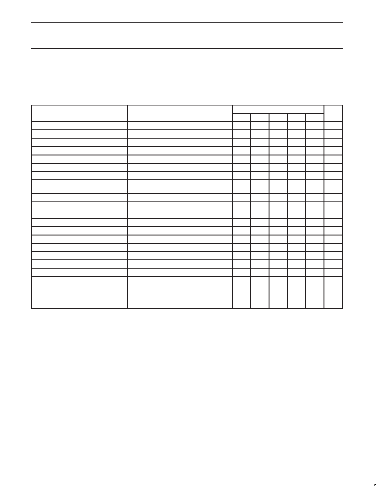
DC CHARACTERISTICS
VCC = 3.3 V; T
Power supply
V
CC
I
CC
I
CC(PD)
Logic inputs (LO_ENABLE, PCS/CEL, S0, S1, LO_X2_EN pins)
V
IH
V
IL
I
IH
I
IL
= +25 °C
amb
Supply voltage all modes 2.7 2.85 3.3 V
Supply current
Supply current in power down Sleep 1 50 µA
HIGH level input voltage range At logic 1 0.5V
LOW level input voltage range At logic 0 –0.3 0.2V
HIGH level input bias current pins at VCC – 0.4 V –5 0 5 µA
LOW level input bias current pins at 0.4 V –5 0 5 µA
PCS1 mode 32.5 37.4 mA
PCS1 Idle mode 21.9 25.2 mA
PCS2 mode 36.9 42.4 mA
PCS2 Idle mode 26.3 30.2 mA
FM mode 22.3 25.6 mA
FM Idle mode 11.8 13.8 mA
LIMITS
MIN TYP MAX
CC
VCC+0.3 V
CC
V
1999 Oct 28
5
Philips Semiconductors Preliminary specification
in ut isolation
and without doubler. 0 dBm LO in, (Tx) LO
SPECIFICATION
CONDITIONS
UNIT
Dual-band, PCS(CDMA)/AMPS
SA9504
LNA and downconverter mixers
LNA
AC ELECTRICAL CHARACTERISTICS
VCC = 2.7 V; T
Cellular band LNA
RF input frequency range 869 894 MHz
Gain 15.5 16.5 17.5 dB
Noise Figure 1.6 1.9 dB
Input IP3
S11 With external matching –10 dB
S22 –15 dB
S12 –40 dB
LO (input and output) to LNA
input isolation
All modes
PCS band LNA
RF input frequency range 1810 1990 MHz
Gain 13.8 14.8 16 dB
Noise Figure 2.0 2.4 dB
Input IP3 2 tones of –30 dBm each, ∆f=800 kHz 0 1.5 dBm
S11 With external matching –9 dB
S22 –12 dB
S12 –40 dB
LO (input and Output) to LNApLO single-ended in, single-ended out, with
= 25°C
amb
PARAMETER TEST CONDITIONS
2 tones of –30 dBm each, ∆f=60 kHz –7 –6 dBm
2 tones of –30 dBm each, ∆f=800 kHz –3 –1.5 dBm
LO single-ended in, single-ended out, with
and without doubler. 0 dBm LO in, (Tx) LO
buffer ON.
MIN
–3σ
LIMITS
TYP +3σ MAX
40 dB
36 dB
UNIT
buffer ON.
TYPICAL LNA SPECIFICATIONS WITH TEMPERATURE VARIATION A T –40°C AND +85°C
VCC = 2.7 V
TEMPERATURE
–40°C +25°C +85°C
Cellular band LNA
Supply current variation –100 0 –100 µA
Gain variation 1 0 –1 dB
Noise Figure variation –0.3 0 0.3 dB
Input IP3 variation ∆f = 60 kHz –0.35 0 0.3 dBm
PCS band LNA
Supply current variation –40 0 –40 µA
Gain variation 0.8 0 –1 dB
Noise Figure variation –0.4 0 0.4 dB
Input IP3 variation 0.9 0 –1 dBm
1999 Oct 28
6
Philips Semiconductors Preliminary specification
PARAMETER
TEST CONDITIONS
UNIT
Dual-band, PCS(CDMA)/AMPS
SA9504
LNA and downconverter mixers
DOWNCONVERTER
AC ELECTRICAL CHARACTERISTICS
VCC = 2.7 V; T
f
= 881 MHz, fLO = 966.4 MHz, fIF = 85.4 MHz, output differential load of 850Ω for FM.
RF
Cellular band downconverter
RF input frequency range 869 894 MHz
LO input frequency range 950 1030 MHz
IF output frequency range 50 300 MHz
IF Output Load Impedance Single-ended, with external balun 850 Ω
Conversion Gain 6.5 7.5 8.2 dB
Noise Figure Single sideband Noise Figure 10 11 dB
Input IP3 P1, P2 = –24 dBm.
RF Input Return Loss ZS=50Ω with external matching 11.0 dB
LO Input Return Loss ZS=50Ω 10.0 dB
(Tx) LO Output Return Loss ZS=50Ω 8.0 dB
LO Input Power Range –9 –6 0 dBm
(Tx) LO Output Power Range ZL=50Ω single-ended; (Tx) LO buffer ON. –6 –3 0 dBm
LO (Input and Output) to RF Leakage Single-ended in, single-ended out. –30 dBm
LO (Input and Output) to IF Leakage Single-ended in, differential out. –20 dBm
RF to LO (Input) Isolation Single-ended in, single-ended out 30 dB
RF to IF Isolation Single-ended in, differential out 10 dB
(Tx) LO Output to LO Input Isolation Single-ended in, differential out 30 dB
Leakage conversion gain f1 = fRX ± 40 MHz at LNA input.
= 25°C, Plo= –3 dBm.
amb
Tone spacing = 60 kHz
P1 = – 70 dBm.
Measured through conversion gain in
stop-band, without SAW filters being
connected. Ports terminated with 50Ω.
MIN
LIMITS
TYP
–3s
5.0 dBm
–40 dBc
+3s
MAX
1999 Oct 28
7
 Loading...