

Philips sa9502 DATASHEETS
INTEGRATED CIRCUITS
SA9502
Dual-band, CDMA/AMPS
downconverter IC
Product specification
Supersedes data of 1998 Dec 10
IC17 Data Handbook
1999 Mar 19
Philips Semiconductors Product specification
SA9502Dual-band, CDMA/AMPS downconverter IC
DESCRIPTION
The SA9502 integrates all the front end receive mixers necessary
for use in dual-band, triple-mode CDMA/AMPS cellular phone
handsets. There are three individual mixer blocks, each optimised
for high linearity with low power consumption for operation in one of
the following modes: High-band 1900MHz PCS CDMA, low-band
800MHz cellular CDMA or analog FM AMPS/TACS modes.
Additionally, the entire circuit can be powered down and put into
sleep mode, reducing the supply current to typically 12 µA. The
circuit has been designed in our advanced QUBiC2 BiCMOS
process with 20GHz f
.
T
FEATURES
•PCS and cellular downconverter mixers typical performance:
– PCS: Gain=1 1.1dB, NF=8.4dB, IIP3= +1.8dBm
– CDMA: Gain=1 1.3dB, NF=9.4dB, IIP3= +5.7dBm
– FM: Gain= 7.5dB, NF=10.5dB, IIP3= +6.2dBm
•Separate, selectable IF outputs to suit FM and CDMA bandwiths
•PCS mixer LO: direct or via internal frequency doubler
•Switchable wideband LO output buffer
•Low voltage operation down to 2.7V
•Low current consumption in “idle”/receive modes:
– PCS : 14.3mA @ 2.7V
– CDMA: 17.6mA @ 2.7V
– FM: 6.8mA @ 2.7V
•Low standby current in sleep mode, typically 12 µA
•TSSOP20 package
APPLICA TIONS
•800MHz analog FM and CDMA digital receivers
•1900MHz PCS band CDMA digital recievers
•Supports dual-mode and triple-mode operation
•Digital mobile communications equipment
•Portable, low power radio equipment
ORDERING INFORMATION
EXTENDED
TYPE NUMBER
SA9502DH 20 TSSOP Plastic thin shrink small outline package; body 6.5 x 4.4 x 1.1 mm SOT360-1
PINS PIN POSITION MATERIAL CODE
PACKAGE
1999 Mar 19 853–2135 21064
2
Philips Semiconductors Product specification
SA9502Dual-band, CDMA/AMPS downconverter IC
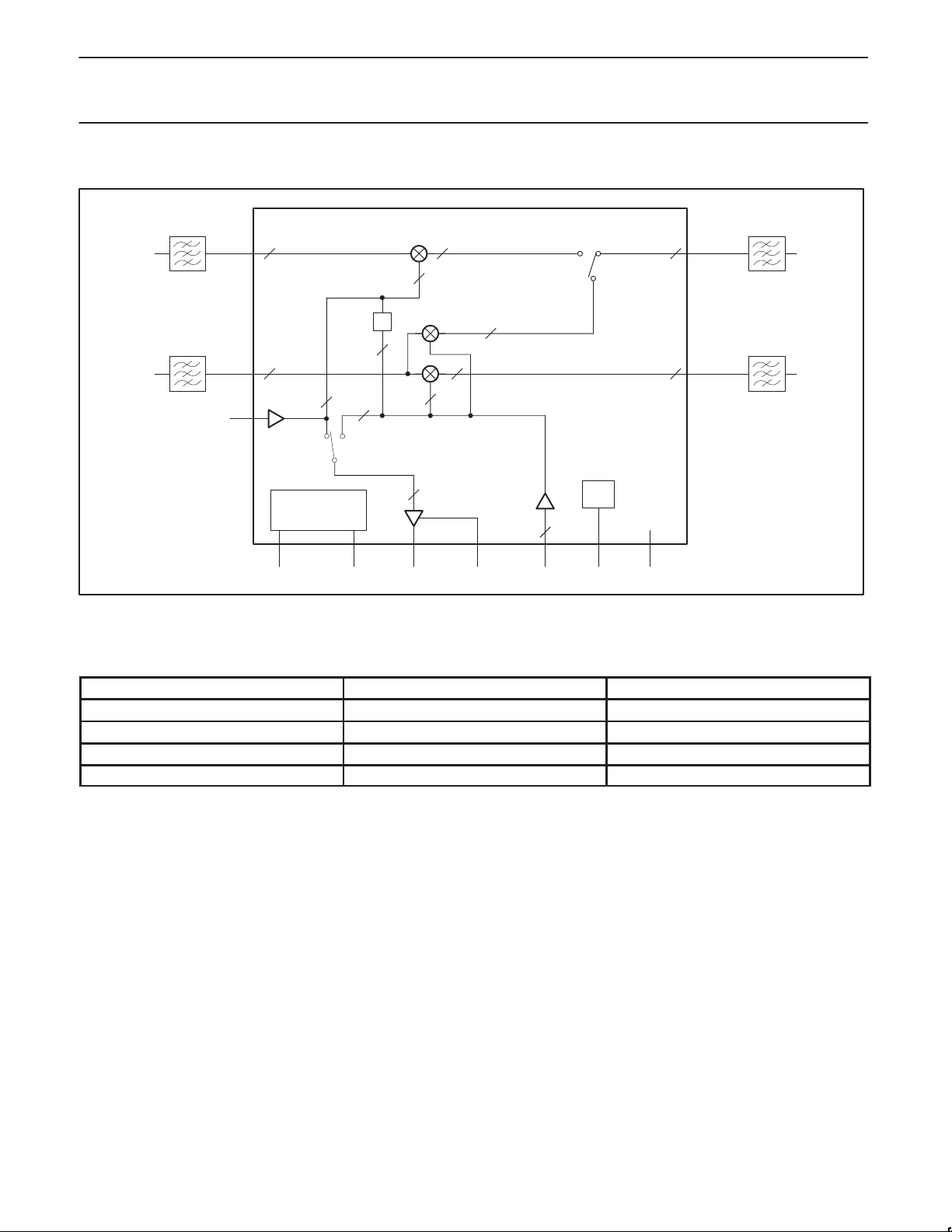
BLOCK DIAGRAM
RX BPF
Fo = 1960 MHz
BW = 60 MHz
PCS_in
RX BPF
Fo = 881.5MHz
BW = 45 MHz
Cell_in
PCS LO
2
×2
2
1
1
1
CELLPCS
MODE
SELECT
LOGIC
CDMA/FM PCS/CELL LO OUT LO BUFFER
2
2
2
2
2
1
ENABLE
Figure 1. Block Diagram
1
CEL
LO IN
PCS
CELL
SA9502
BIAS
CTRL
V
CC
2
2
PWR ON/OFF
CDMA IF BPF
Fo = 85.38MHz
BW = 1.23MHz
CDMA_Out
FM_Out
FM IF BPF
Fo = 85.38MHz
BW = 30kHz
SR01718
Table 1. Mode Selection Summary
PCS/CEL (Pin 6) CDMA/FM/LO doubler (Pin 17) MODE
low low Cellular FM
low high Cellular CDMA
high low CDMA PCS, direct LO in
high high CDMA PCS, LO via frequency doubler
1999 Mar 19
3
Philips Semiconductors Product specification
SA9502Dual-band, CDMA/AMPS downconverter IC
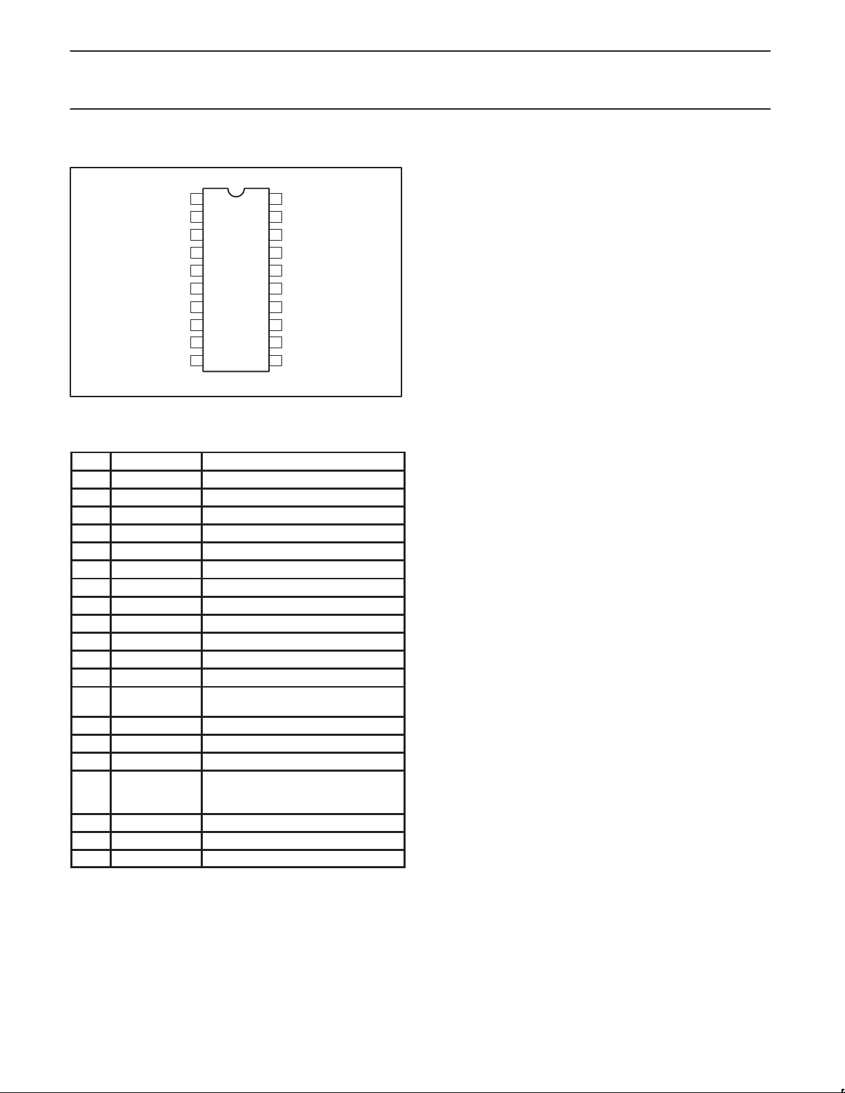
PIN CONFIGURATION
1
2
FM IFB
3
GND
4
PCS RF
CEL RF
GND
V
5
6
7
8
9
CC
PCS RFB
PCS/CEL SEL
PWR ON/OFF
Figure 2. Pin Configuration
20FM IF
19
18
17
16
15
14
13
12
11
SR01760
CDMA IF
CDMA IFB
GND
CDMA/FM SEL
CEL LO IN
GND
PCS LO
LO BUFFER ENABLE
GND
LO OUT10
PIN DESCRIPTION
PIN SYMBOL DESCRIPTION
1 FM IF Non-inverting FM IF output
2 FM IFB Inverting FM IF output
3 GND Analog ground
4 PCS RF non-inverting PCS RF input
5 PCS RFB Inverting PCS RF input
6 PCS/CEL SEL PCS and cellular band select
7 PWR ON/OFF Power enable
8 CEL RF Cellular RF input
9 GND Ground
10 V
CC
11 LO OUT LO output to synthesizer
12 GND Ground
13 LO BUFFER
ENABLE
14 PCS LO PCS mixer direct LO input
15 GND Ground
16 CEL LO Cellular LO input
17 CDMA/FM SEL CDMA and FM mode select in cellular
18 GND Ground
19 CDMA IFB Inverting CDMA IF output
20 CDMA IF Non-inverting CDMA IF output
Power supply
Logic signal which switches the LO
buffer output ON or OFF
band; LO direct or via frequency
doubler in PCS mode
FUNCTIONAL DESCRIPTION
Mode Selection Logic
The SA9502 downconverter IC has several modes of operation for
which the selection logic is summarized in Table 1 and defined in
detail in Table 2. Different mode selections require different portions
of the circuit to be active. It should be noted that only the states
specified in Table 2 are valid selections for operation.
Local Oscillator Section
Local oscillator drive for the mixers is provided through single ended
inputs on either pin 16 (CEL LO) or pin 14 (PCS LO). The LO signal
has to be AC-coupled into the circuit and needs to be externally
matched. Inside the circuit, the cellular band LO signal is amplified
and buffered to drive: Either the cellular CDMA mixer or FM mixer
or the frequency doubler for the PCS mixer LO and additionally the
LO output buffer. The mode selection summary in Table 1 shows the
logic to apply to pins 6 and 17 to choose one of four possible
modes. The LO output buffer can be programmed on or off via LO
Buffer Enable (Pin 13). The LO output buffer’s frequency is the
same as that used by the mixers.
Cellular and PCS Mixers
The SA9502 has one single ended cellular band RF input which
feeds either the cellular CDMA mixer or the cellular FM mixer
circuits. Each mixer is optimized to meet cellular band CDMA or
analog FM requirements. The cellular FM mixer has its own
dedicated differential output on pins 1 and 2 which should to be
externally matched to the FM IF SAW filter . The cellular CDMA
mixer shares the same output pins with the CDMA PCS mixer.
Selection between these two mixers is via pin 6 (PCS/CEL) and as
the two mixers are never on at the same time, it allows a common
CDMA SAW filter to be used for both bands. The CDMA PCS mixer
has a differential RF input which should be used with an external
balun matching circuit. To avoid upsetting the internal biasing, the
RF inputs at both cellular and PCS band mixers should be
AC-coupled in. The CDMA and FM IF mixer outputs are of the open
collector type. So, they should be biased to the supply voltage V
with external tuning inductors which can also serve in the matching
of the IF SAW filter.
CC
1999 Mar 19
4
Philips Semiconductors Product specification
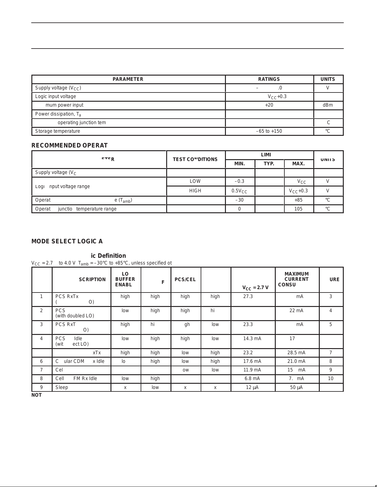
PARAMETER
TEST CONDITIONS
ÁÁÁÁ
UNITS
ÁÁÁÁ
ÁÁÁÁ
Logic i
ÁÁÁÁ
ÁÁÁÁ
ÁÁÁÁ
SA9502Dual-band, CDMA/AMPS downconverter IC
ABSOLUTE MAXIMUM RATINGS
PARAMETER
Supply voltage (VCC)
Logic input voltage
Maximum power input
Power dissipation, T
amb
=25°C
Maximum operating junction temperature
Storage temperature
RECOMMENDED OPERATING CONDITIONS
Supply voltage (VCC)
nput voltage range
Operating ambient temperature range (T
Operating junction temperature range
amb
)
LOW
HIGH
MIN.
2.7
–0.3
0.5V
–30
0
RATINGS
–0.3 to +6.0
–0.3 to VCC+0.3
–65 to +150
LIMITS
CC
+20
800
150
TYP.
3.0
MAX.
4.0
0.2V
CC
VCC+0.3
+85
105
UNITS
V
V
dBm
mW
°C
°C
V
V
V
°C
°C
MODE SELECT LOGIC AND DC CHARACTERISTICS
Table 2. Mode Logic Definition
VCC = 2.7 V to 4.0 V; T
MODE
MODE DESCRIPTION
1 PCS RxTx
(with doubled LO)
2 PCS Idle
(with doubled LO)
3 PCS RxTx
(with direct LO)
4 PCS Rx Idle
(with direct LO)
5 Cellular CDMA RxTx high high low high 23.2 mA 28.5 mA 7
6 Cellular CDMA Rx Idle low high low high 17.6 mA 21.0 mA 8
7 Cellular FM RxTx high high low low 1 1.9 mA 15.5 mA 9
8 Cellular FM Rx Idle low high low low 6.8 mA 7.8 mA 10
9 Sleep x low x x 12 µA 50 µA
NOTE:
x = Don’t care
= –30°C to +85°C, unless specified otherwise.
amb
LO
BUFFER
ENABLE
POWER
ON/OFF
high high high high 27.3 mA 33 mA 3
low high high high 18.4 mA 22 mA 4
high high high low 23.3 mA 28 mA 5
low high high low 14.3 mA 17 mA 6
PCS/CEL CDMA/FM
TYPICAL
CURRENT
CONSUMPTION
= 2.7 V
@ V
CC
MAXIMUM
CURRENT
CONSUMPTION
FIGURE
1999 Mar 19
5
Philips Semiconductors Product specification
PARAMETER
TEST CONDITIONS
UNITS
IF output load impedance
Conversion gain
Noise figure
j
j
SA9502Dual-band, CDMA/AMPS downconverter IC
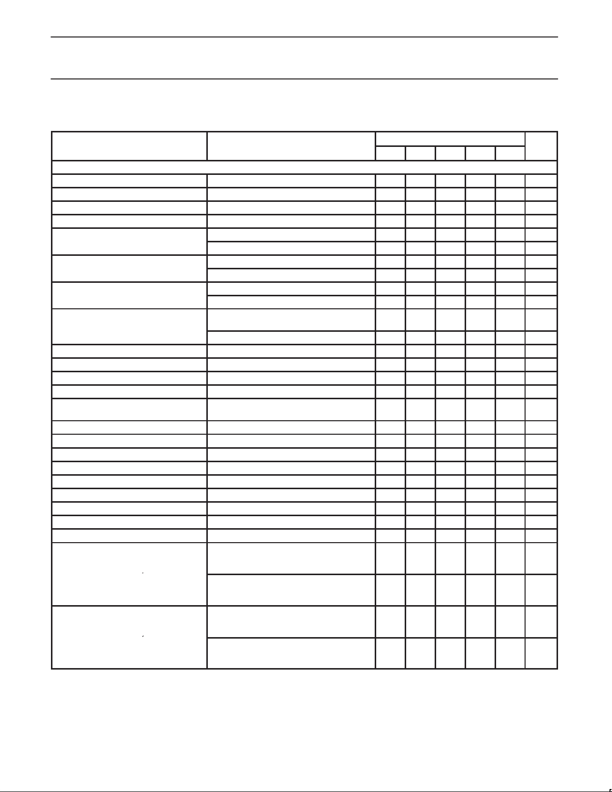
AC ELECTRICAL CHARACTERISTICS
VCC = 2.7V; T
Cellular Band Downconverter
RF input frequency range 869 894 MHz
LO input frequency range 950 1030 MHz
IF output frequency range (CDMA) 50 300 MHz
IF output frequency range (FM) 50 300 MHz
Input IP3
RF input return loss ZS = 50Ω 11.0 dB
LO input return loss ZS = 50Ω 10.0 dB
LO output return loss ZS = 50Ω 8.0 dB
LO input power range –6.0 –3.0 0.0 dBm
LO output power range
LO (input and output) to RF leakage Single-ended in, single-ended out –34.5 –31.5 dBm
LO (output) to IF leakage (CDMA) Single-ended in, differential out –33.6 –29.0 dBm
LO (output) to IF leakage (FM) Single-ended in, differential out –20.0 –17.5 dBm
LO (input) to IF leakage (CDMA) Single-ended in, differential out –27.7 –26.5 dBm
LO (input) to IF leakage (FM) Single-ended in, differential out –18.5 –17.8 dBm
RF to LO (input) isolation Single-ended in, single-ended out 30 32.8 dB
RF to IF isolation (CDMA) Single-ended in, differential out 17 17.7 dB
RF to IF isolation (FM) Single-ended in, differential out 6 8.2 dB
LO output to LO input isolation Single-ended in, single-ended out 26.5 33 dB
Spurious response rejection
(CDMA mode)
Spurious response rejection
(FM mode)
= +25°C; Plo = –3 dBm, fIF = 85.40 MHz and measured on Philips demonstration board; unless specified otherwise.
amb
MIN. –3σ TYP. +3σ MAX.
p
p
CDMA, differential 1000 Ω
FM, single-ended, with ext. balun 850 Ω
CDMA 10.7 11.3 11.9 dB
FM 7.0 7.5 8.0 dB
CDMA mode, SSB 9.4 10.0 dB
FM mode, SSB 10.5 10.7 dB
CDMA mode, tone spacing = 900 kHz and
1.7 MHz
FM mode, tone spacing = 60 kHz 5.3 6.2 dBm
ZL = 50Ω, single LO out
with LO buffer on (Pin 13 = High)
With Tx band interferer at LO input port or
LO buffer output port of –40 dBm max and
with Pint = –31 dBm in Rx band.
With Tx band interferer at RF input port of
–40 dBm max and with Pint = –31 dBm in
Rx band.
With Tx band interferer at LO input port or
LO buffer output port of –40 dBm max and
with Pint = –31 dBm in Rx band.
With Tx band interferer at RF input port of
–40 dBm max and with Pint = –31 dBm in
Rx band.
4.8 5.7 dBm
–7.5 –5.0 –3.0 dBm
43 44 dB
59 61 dB
43 44 dB
55 56 dB
1999 Mar 19
6
Philips Semiconductors Product specification
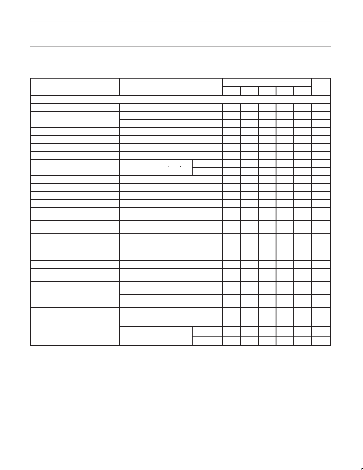
PARAMETER
TEST CONDITIONS
UNITS
LO input frequency range
Input IP3
IF
,qy
1/2 IF supurious rejection
Spurious response rejection
in ut ort of –40 dBm max and
SA9502Dual-band, CDMA/AMPS downconverter IC
AC ELECTRICAL CHARACTERISTICS (continued)
VCC = 2.7V; T
PCS Downconverter
RF input frequency range 1810 1990 MHz
IF output frequency range 50 300 MHz
IF output load impedance Differential 1000 Ω
Conversion gain @ fIF, over RF/LO frequency ranges 10.5 11.1 11.7 dB
Noise figure @ fIF, over RF/LO frequency ranges, SSB 8.4 9.3 dB
p
RF input return loss ZS = 50Ω, with external balun 7.5 dB
LO input return loss ZS = 50Ω 10 dB
LO output return loss ZS = 50Ω, single LO out 8 dB
LO input power range –6 –3 0 dBm
LO output power range
LO (input and output) to RF leakage
LO (input and output) to IF leakage
RF to LO (input) isolation
RF to IF isolation Single-ended in, dif ferential out 32 40 dB
LO output to LO input isolation
p
= +25°C; Plo = –3 dBm, fIF = 85.40 MHz and measured on Philips demonstration board; unless specified otherwise.
amb
MIN –3σ TYP. +3σ MAX.
p
p
With doubler 860 1050 MHz
Direct PCS LO 1720 2200 MHz
@ fIF, over RF/LO frequency
ranges at 25°C @ VCC = 3.6V
ZL = 50Ω, single LO out with LO buffer on
(Pin 13 = High)
Single-ended in, single-ended out,
with and without doubler
Single-ended in, differential out,
with and without doubler
Single-ended in, single-ended out,
with and without doubler
Single-ended in, single-ended out,
with doubler
1/2 IF spur, fIF = 85.4 MHz/111.38 MHz,
with doubler, P
= –30 dBm at RF input.
int
1/2 IF spur, fIF = 85.4 MHz/111.38 MHz,
without doubler, P
= –30 dBm at RF input.
int
direct LO 0.5 1.8 dBm
doubled LO 0.1 1.2 dBm
–10.0 –8.5 –7 dBm
–56 –47 dBm
–43 –39 dBm
44 46 dB
30 31 dB
42 46 dB
68 76 dB
With Tx band interferer at LO input port or LO
buffer output port of –40 dBm max and with
= –21 dBm in Rx band.
P
p
int
With Tx band interferer at RF
p
p
with P
= –21 dBm in Rx band. doubled LO 53 61 dB
int
direct LO 59 64 dB
43 44 dB
1999 Mar 19
7
Philips Semiconductors Product specification
SA9502Dual-band, CDMA/AMPS downconverter IC
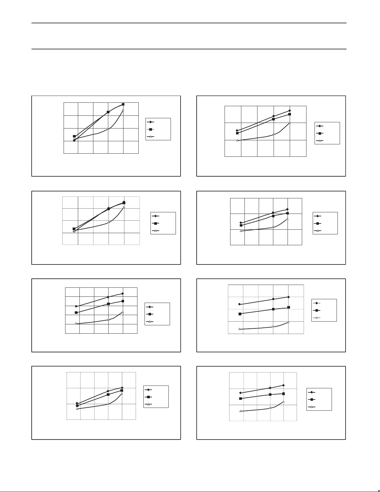
PERFORMANCE CHARACTERISTICS
DC Current Consumption
30.0
29.0
28.0
27.0
CURRENT (mA)
26.0
2.4 2.8 3.2 3.6 4.0 4.4
VCC (V)
SR01825
Figure 3. PCS RxTx (with doubled LO out) current
26.0
25.0
24.0
23.0
CURRENT (mA)
22.0
2.4 2.8 3.2 3.6 4 4.4
VCC (V)
Figure 5. PCS RxTx current
–30°C
+25°C
+85°C
–30°C
+25°C
+85°C
SR01827
20.0
19.0
18.0
CURRENT (mA)
17.0
2.4 2.8 3.2 3.6 4 4.4
VCC (V)
Figure 4. PCS Idle (with doubled LO out) current
16.0
15.0
14.0
CURRENT (mA)
13.0
2.4 2.8 3.2 3.6 4 4.4
(V)
V
CC
Figure 6. PCS Rx Idle current
–30°C
+25°C
+85°C
SR01826
–30°C
+25°C
+85°C
SR01828
26.0
25.0
24.0
23.0
CURRENT (mA)
22.0
21.0
2.4 2.8 3.2 3.6 4 4.4
VCC (V)
Figure 7. Cellular CDMA RxTx current
14.0
13.0
12.0
CURRENT (mA)
11.0
2.4 2.8 3.2 3.6 4 4.4
(V)
V
CC
Figure 9. Cellular FM RxTx current
–30°C
+25°C
+85°C
SR01829
–30°C
+25°C
+85°C
SR01831
20.0
19.0
18.0
17.0
CURRENT (mA)
16.0
2.4 2.8 3.2 3.6 4 4.4
VCC (V)
Figure 8. Cellular CDMA Rx Idle current
7.5
7.0
6.5
CURRENT (mA)
6.0
2.4 2.8 3.2 3.6 4 4.4
VCC (V)
Figure 10. Cellular FM Rx Idle current
–30°C
+25°C
+85°C
SR01830
–30°C
+25°C
+85°C
SR01832
1999 Mar 19
8
 Loading...