

Philips SA9025 Datasheet

INTEGRATED CIRCUITS
SA9025
900 MHz transmit modulator and
2.2 GHz fractional–N synthesizer
Objective specification 1997 Aug 01
Philips Semiconductors Objective specification
900 MHz transmit modulator and 2.2 GHz
fractional–N synthesizer
DESCRIPTION
This specification defines the requirements for a transmitter
modulator and fractional–N synthesizer IC to be used in cellular
telephones which employ the North American Dual Mode Cellular
System (IS–136).
FEA TURES
•Low current from 3.75V supply
•Low phase noise
•Main loop with internal charge pump and fractional compensation
•3–line serial interface bus
•Power down for the synthesizers
•Speedup mode for faster switching
APPLICATIONS
•Cellular phones
•Portable battery–powered radio equipment.
GENERAL DESCRIPTION
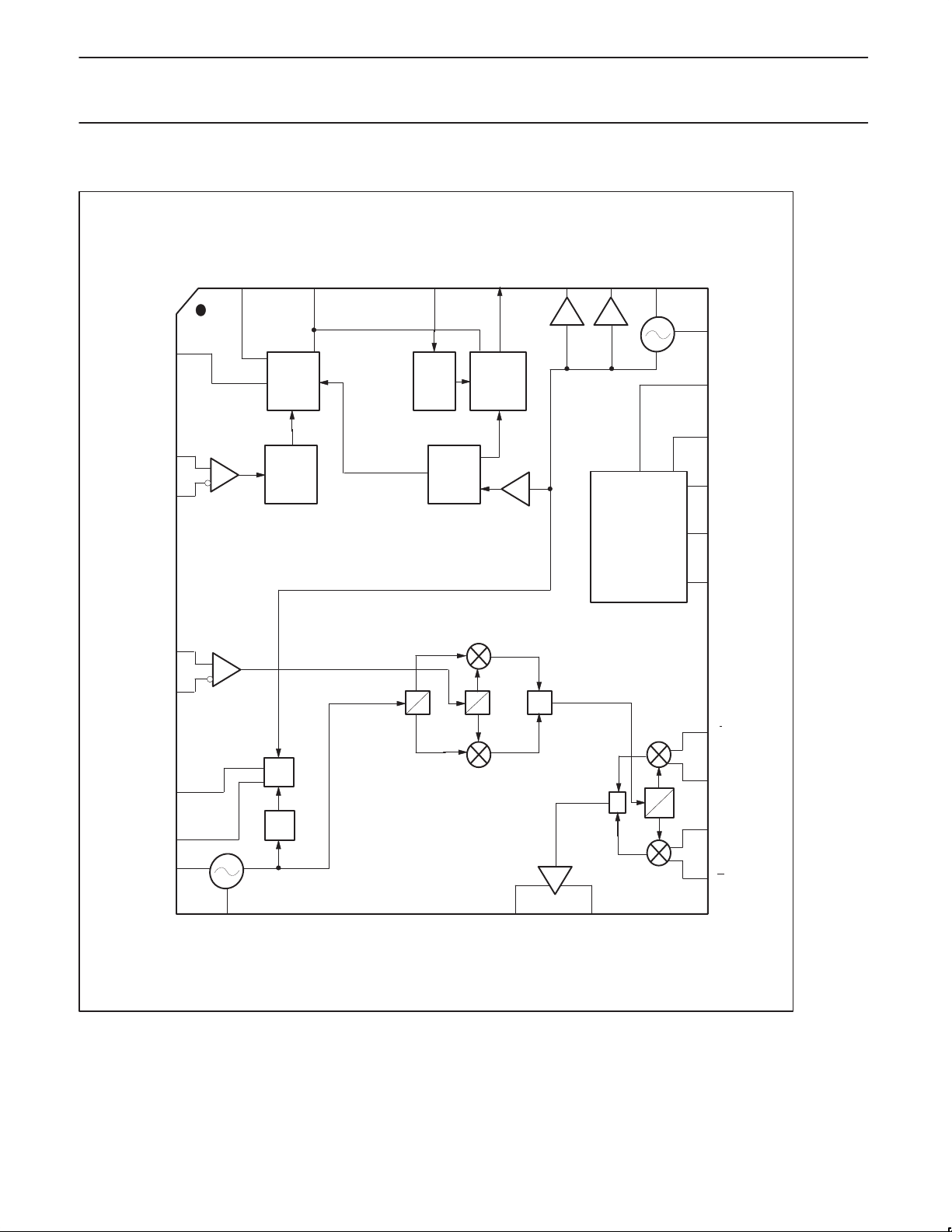
The SA9025 BICMOS device integrates:
•Main channel synthesizer
•Auxiliary synthesizer
•Transmit offset synthesizer and oscillator
•I/Q modulator
•Power control
SA9025
•Reference and clock buffers
•Control logic for programming and power down modes
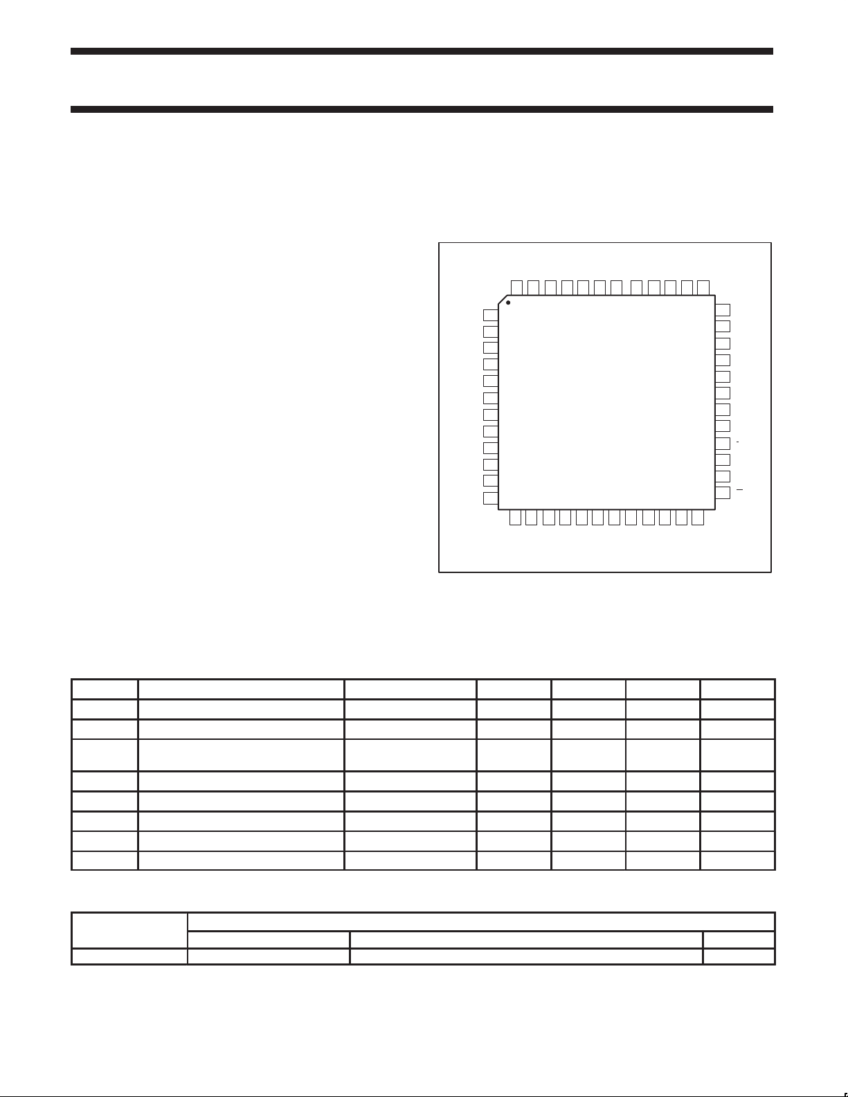
PIN CONFIGURATION
CC
V
PHA
TX1
DUAL
GND
RCLK
394041 3738
TX2
DUAL
GND
20 21 22 23 24
GND
MCLK
GND
Vcc
PHP
V
CC
RX
RX
GND
V
CC
TX
TX
GND
PHS out
Ipeak
TANK1
LO1
LO2
LO1
LO2
PHI
GNDRNGND
1
2
3
4
5
6
7
8
9
10
11
12
13 14 15 16 17 18 19
Vcc
GND
TANK2
Figure 1. Pin Configuration
45464748
GND
CC
INA
V
424344
SA9025
GND
GND
1
XTAL
36
XTAL
2
35
TX
EN
34
DATA
33
CLOCK
32
LOCK
31
STROBE
30
GND
29
V
CC
28
I
27
I
26
Q
25
Q
SR01446
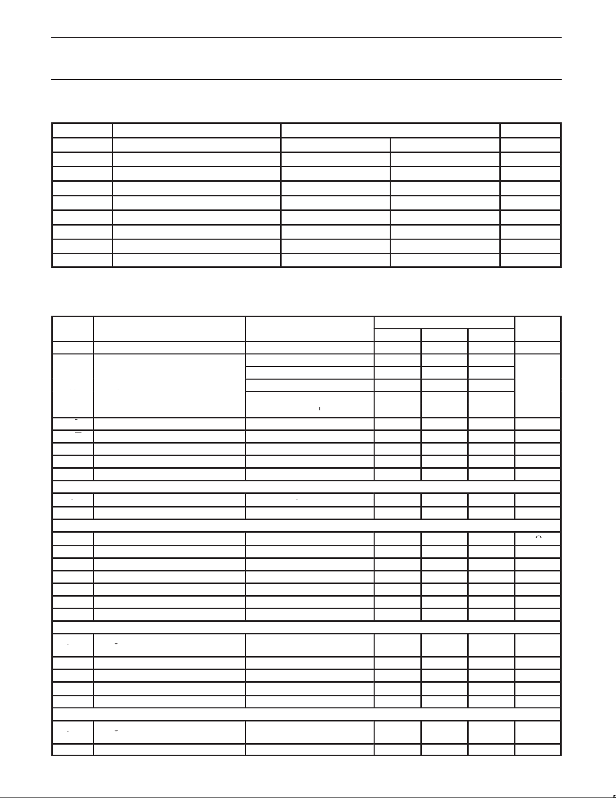
QUICK REFERENCE DATA
SYMBOL PARAMETER CONDITIONS MIN. TYP. MAX. UNIT
V
CC
I
CC
I
CC_save
f
VCO
f
AUX
f
XTAL
f
PC
T
amb
Supply voltage V
CC
3.6 3.75 3.9 V
Supply current – TBD – mA
Total supply current in power–down
– TBD – mA
mode
Input frequency 800 – 2200 MHz
Input frequency 10 – 500 MHz
Crystal reference input frequency 10 – 40 MHz
Maximum phase comparator frequency Main and Aux loops – – 5 MHz
Operating ambient temperature –40 – +85 °C
ORDERING INFORMATION
TYPE NUMBER
NAME DESCRIPTION VERSION
SA9025 LQFP48 Plastic low profile quad flat package; 48 leads; body 7x7x1.4 mm SOT313-2
PACKAGE
1997 Aug 01
2
Philips Semiconductors Objective specification
900 MHz transmit modulator and 2.2 GHz
fractional–N synthesizer
CONNECTIONS
GND
CC
INA
V
AUX.
DIV.
÷A
REF.
DIV.
RX
RX
PHP
V
CC
LO1
LO2
GND
PHI
GND
MAIN PD
and CP
MAIN
DIV.
÷N
RN
GND
PHA
AUX PD
and CP
SA9025
1
CC
RCLK
MCLK
CONTROL
LOGIC
XTAL
XTAL
2
TX
EN
DATA
CLOCK
LOCK
V
V
CC
TX
LO1
TX
LO2
GND
PHS out
Ipeak
TANK1
TANK2
STROBE
GND
V
CC
I
I
Q
Q
SR01455
GND
0
GND
TX1
DUAL
∑
0
GND
∑
TX2
DUAL
GND
90
CC
V
90
0
90
∅
÷M
CC
V
GND
GND
GND
Figure 2. SA9025 Block Diagram
1997 Aug 01
3
Philips Semiconductors Objective specification
900 MHz transmit modulator and 2.2 GHz
fractional–N synthesizer
PIN DESCRIPTIONS
PIN
NO.
1 PHP Proportional charge pump output
2 V
3 RX
4 RX
5 GND Digital Ground
6 V
7 TX
8 TX
9 GND Tank Ground
10 PHS OUT Charge pump output (transmit offset)
11 I
12 TANK1 VCO differential tank
13 TANK2 VCO differential tank
14 V
15 GND Tx Ground
16 GND Tx Ground
17 GND Tx Ground
18 GND Tx Ground
19 GND Tx Ground
20 DUALTX1 Dual mode RF output
21 GND Tx Ground
22 DUALTX2 Dual mode RF output
23 GND Tx Ground
PIN DESCRIPTION
CC
CC
PEAK
CC
Digital supply voltage
Differential LO input
LO1
Differential LO input
LO2
Tank supply voltage
Differential Transmit LO Input
LO1
Differential Transmit LO Input
LO2
PHS out current set resistor
Tx supply voltage
SA9025
24 V
25 Q Inverting quadrature input
26 Q Non–Inverting quadrature input
27 I Non–inverting in phase modulation input
28 I Inverting in phase modulation input
29 V
30 GND Tx Ground
31 STROBE Data input latch enable
32 LOCK Lock detect
33 CLOCK Serial clock input
34 DAT A Serial data input
35 TX
36 XTAL
37 XTAL
38 MCLK Buffered oscillator output
39 RCLK Buffered oscillator output
40 V
41 PHA Auxiliary charge pump output
42 GND REF Ground
43 INA RX
44 V
45 GND CP Ground
46 RN CP current set resistor
47 GND CP Ground
48 PHI Integral charge pump output
Tx supply voltage
CC
Tx supply voltage
CC
Transmit enable
EN
Crystal Oscillator emitter input
2
Crystal Oscillator base Input
1
REF supply voltage
CC
input
IF
CP supply voltage
CC
1997 Aug 01
4
Philips Semiconductors Objective specification
900 MHz transmit modulator and 2.2 GHz
fractional–N synthesizer
OPERATING MODES & POWER DOWN CONTROL
There are two power saving modes of operation which the SA9025
can be put into, dependent on the status of the system. The
intention of these different modes is to disable circuity that is not in
use at the time in order to reduce power consumption. During sleep
mode, only circuitry which is required to provide a master clock to
SA9025 POWER MODE TRUTH TABLE
Enabled yes no yes no yes no
Crystal Oscillator
Phase detector and charge pump (transmit offset)
VCO
SSB Up-converter
MCLK Buffer
RCLK Buffer
÷M offset loop divider
TXLO Buffer
RXLO Buffer
I/Q Modulator
Variable Gain Amp.
Control Logic
Main Divider
Reference Divider
Auxiliary Divider
Main Phase Detector and charge pump
Auxiliary Phase Detector and charge pump
Lock Detect
SA9025
the digital portion of the system is enabled. During receive mode,
circuitry which is used to perform the receive function and provide a
master clock is enabled. In transmit mode all the functions of the
chip are enabled which are required to perform transmit, receive and
provide master clock.
Sleep Mode Receive Mode Transmit Mode
✓ ✓ ✓
✓ ✓ ✓
✓ ✓ ✓
✓ ✓ ✓
✓ ✓ ✓
✓ ✓ ✓
✓ ✓ ✓
✓ ✓ ✓
✓ ✓ ✓
✓ ✓ ✓
✓ ✓ ✓
✓ ✓ ✓
✓ ✓ ✓
✓ ✓ ✓
✓ ✓ ✓
✓ ✓ ✓
✓ ✓ ✓
✓ ✓ ✓
1997 Aug 01
5
Philips Semiconductors Objective specification
PARAMETER
TEST CONDITIONS
UNITS
CC
y
DUAL
1
52
VOLOutput voltage LOW
I
2mA
0.4
V
RN
External resistor to ground
6
7.5
24
k
I
g
1515%
I
g
1515%
900 MHz transmit modulator and 2.2 GHz
fractional–N synthesizer
ABSOLUTE MAXIMUM RATINGS
SYMBOL PARAMETER VALUE UNIT
MIN. MAX.
V
CC
V
IN
P
N
T
JMAX
P
MAX
I
MAX
T
STG
T
o
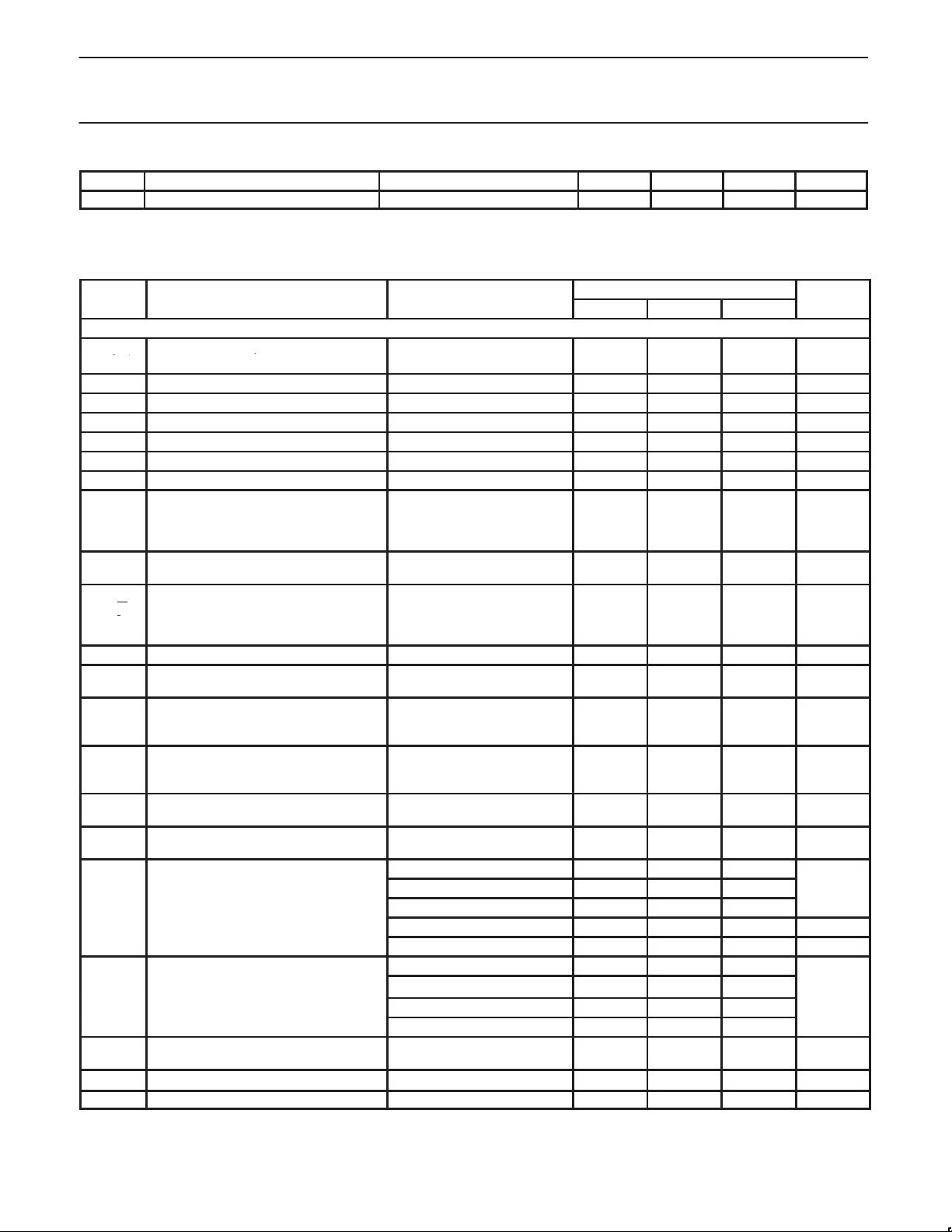
DC ELECTRICAL CHARACTERISTICS
V
= +3.75 V; TA = 25°C; unless otherwise stated.
CC
SYMBO
L
V
CC
I
CC
Supply voltage -0.3 +4.5 V
Voltage applied to any other pin -0.3 VCC+0.3 V
Power dissipation, TA = 25°C (still air) 980 mW
Operation junction temperature TBD °C
Power input/output +10/+14 dBm
DC current into any I/O pin -10 +10 mA
Storage temperature –65 +150 °C
Operating temperature -40 +85 °C
LIMITS
MIN TYP MAX
Power supply range 3.6 3.75 3.9 V
Sleep mode 2
Standby mode 17
Supply current
Operating: full power analog 95
Operating: full power digital
SA9025
mA
I / I In-phase dif ferential input quiescent VCC /2 V
Q / Q Quadrature phase differential input quiescent VCC /2 V
V
Clock, Data, Strobe, TX
IL
V
Clock, data, strobe, TX
IH
T
Ambient temperature range -40 +25 +85 °C
A
EN
EN
Input logic low –0.3 0.3 × V
Input logic high 0.7 × V
CC
VCC+0.3 V
CC
Digital Outputs Lock
p
V
Output voltage HIGH IO = -2mA V
OH
Charge Pump Current Setting Resistor Input; RN, R
R
V
V
I
peak
PHS
External resistor to ground 4.7
Ipeak
Regulated voltage
RN
Regulated voltage
Ipeak
PHSOUT programming
PHSOUT gain
gain
PD phase gain Transmit offset PLL in phase lock 4.33 mA/rad
K
Ipeak
=
O
RN = 7.5 k
R
= 4.7 k
ipeak
R
= 4.7 k
ipeak
R
= 4.7 k
ipeak
– 0.4 V
CC
1.23 V
1.3 V
0.26 mA
24xI
peak
Charge Pump Outputs (including fractional compensation pump, not PHS) RN = 7.5 k
OPH
I
MATCH
Charge pump output current error
versus expected current.
Sink to source current matching V
Current output variation versus V
Charge pump off, leakage current V
V
Charge pump voltage compliance
PH
Charge Pump Outputs (only PHS) R
OPH
I
MATCH
Charge pump output current error
versus expected current.
Sink to source current matching V
ipeak
PHX
3
= 4.7 k
VCC/2 –5 5 %
PHX =
V
in compliance range –10 10 %
PHX
= VCC/2 –10
PHX
= VCC/2 –10 10 %
PHS
–
1
10 nA
0.7 VCC – 0.8 V
–
V
k
mA
1997 Aug 01
6
Philips Semiconductors Objective specification
SYMBOL
PARAMETER
TEST CONDITIONS
UNITS
TX
(
DUAL
TX
conversion roducts
dBc
DUAL
Adjacent channel noise power
@ 30 kH
95
dBc/H
900 MHz transmit modulator and 2.2 GHz
fractional–N synthesizer
Current output variation versus V
V
Charge pump voltage compliance 0.5 VCC–0.5 V
PH
PH
AC ELECTRICAL CHARACTERISTICS
VCC = +3.75 V; TA = 25°C; unless otherwise stated.
Modulator
Transmit LO input (AC-coupled; 50Ω Input power -13 -10 dBm
LO 1/2
single-ended, 100Ω differential) Frequency range 900 1100 MHz
VSWR 2:1
TANK1/2 VCO tank differential inputs Frequency range 90 180 MHz
÷M PLL offset divider Maximum input frequency 180 MHz
XTAL1Osc. transistor base Osc. frequency 10 40 MHz
XTAL2Osc. transistor emitter Osc. frequency 10 40 MHz
XO Negative resistance –100
Reference buffer output
RCLK,
MCLK
TX
Q / Q
I / I
TX
DUAL
DUAL
DUAL
DUAL
DUAL
DUALTXSpurious output 849 to 869 MHz -45
DUAL
DUALTXAlternate channel noise power @ 60 kHz –101 dBc/Hz
Frequency range
Output levels
Harmonic content
Transmit enable
EN
Baseband in-phase differential inputs
TX
RF
TX
operating range 820 920 MHz
RF
DUAL output SE=1, TXEN=1 (with
external matching) (50Ω)
Differential output, (DUALTX)
open-collector, matched to 200Ω
TX
differential impedance
Linearity worst case intermod. products
(0dB VGA OR +9 dBm, whichever is
TX
less, I & Q in-phase)
Carrier suppression
TX
(I & Q in quadrature)
Sideband suppression
TX
(I & Q in quadrature)
p
TX
TX
TX
u-
LO
Broad-band noise (0dB VGA or +9 dBm,
whichever is less)
p
p
V
in compliance range –25 25 %
PHS
LIMITS
MIN TYP MAX
Z
= 5kΩ| | 7 pF
LOAD
Transmit enable
Transmit disable
Maximum frequency
Diff. mod. level
Diff. input impedance
DC bias point
10
0.7
1.8
0.8
10.0
1.8
TX
TX
VCC/2
1.0
EN
EN
0.9
= 1
= 0
AMPS/DAMPS 820 853 MHz
Output level (avg. min., I and Q
+9.0 +11.0
quad., 0dB VGA)
Gain flatness
3rd-order
5th-order
7th-order
VGA = 0dB
VGA = -38dB
1
-42
-55
-65
-45
-33
-45 -35 dBc
2 to 284 MHz -45
824 to 849 MHz -47 dBc
869 to 894 MHz -104 dBm
894 to 8490 MHz -45 dBc
TX
LO
Upper Side Band –21
TXLO ±3 × TX
OFFSET
Harmonics ≤ 10th -21
869 to 894 MHz -123 dBm/Hz
z -
SA9025
40
1.4
–10
1.0
2.55
+13.0 dBm
-34
-45
-53
-35
-21
-36
MHz
V
Logic
MHz
V
P–P
dBc
P-P
kΩ
V
dB
dBc
dBc
z
1997 Aug 01
7
 Loading...