Philips SA900BE Datasheet

INTEGRATED CIRCUITS
SA900
I/Q transmit modulator
Preliminary specification 1997 Sept 16
IC17 Data Handbook

Philips Semiconductors Preliminary specification
SA900I/Q transmit modulator
DO NOT DISTRIBUTE WITHOUT ECN DATED AFTER Sept 16, 1997
DESCRIPTION
The SA900 is a monolithic high performance, multi-function transmit
modulator for use in cellular radio applications, fabricated in QUBiC
BiCMOS technology. The SA900 features both analog (AMPS)
mode and complex, I/Q digital (NADC IS–136) mode quadrature
modulation functions, a PLL synthesizer with VCO, crystal oscillator,
programmable prescalers and Gilbert cell multiplier phase detector
with programmable charge pump output. The DUALTX output can
be used in DUAL mode cellular phone applications with the AMPS
and NADC modulation being applied to the I/Q baseband inputs.
The DUALTX output also provides 6-bit power control with 40dB of
gain control in 0.63dB steps. In addition, buffered crystal oscillator
programmable prescaler outputs are provided to support system
clock reference needs. Programming of the SA900 functions are
realized by a high speed 3-wire serial interface. The SA900 can be
programmed into a sleep mode (low current mode providing crystal
oscillator and Master Clock functions), a standby mode (providing
crystal oscillator, Master Clock, System Clock 1 and Transmit LO
buffer functions), and the AMPS mode and the DUAL mode
configurations.
FEA TURES
•V
= 4.0V
CC
•Tx output frequency = 900MHz
•Direct modulation of RF
•DUAL mode, on-chip PA control
•I/Q modulator
•Single sideband quadrature LO generation with no external
adjustments required
•On-chip crystal oscillator with 3 buffered outputs
•AMPS/TACS compatible
•On-chip VCO
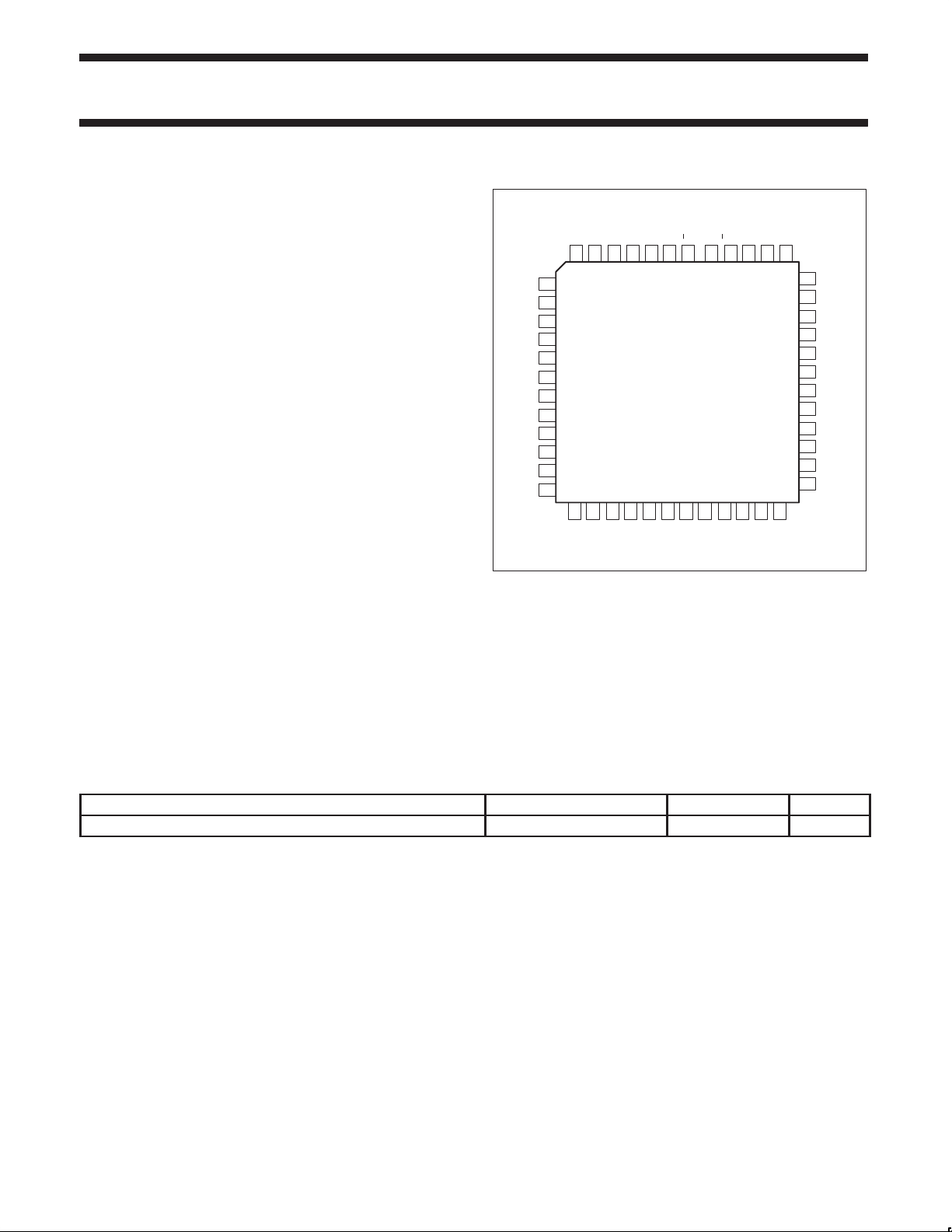
PIN CONFIGURATION
BE Package
I
Vcc
CLK2
GND
I
QQGND
424344
20 21 22 23 24
DATA
MCLK
CLKSET
394041 3738
CLOCK
GND
TXLO_2
TXLO_1
GND
Vcc
TANK_1
TANK_2
Vcc
PHSOUT
I
PEAK
GND
XTAL_1
Vcc
LO_2
LO_1
1
2
3
4
5
6
7
8
9
10
11
12
13 14 15 16 17 18 19
Vcc
CLK1
XTAL_2
GND
45464748
GND
Figure 1. Pin Configuration
•Selective power-down
– Low power AMPS/TACS mode
– Low power dual mode NADC
•48-Pin TQFP package
APPLICATIONS
•North American Digital Cellular (TDMA IS-136)
Vcc
GND
TXEN
STROBE
36
35
34
33
32
31
30
29
28
27
26
25
Vcc
GND
DUALTX
GND
Vcc
AMPSTX
GND
Vcc
GND
Vcc
Vcc
GND
SR00636
ORDERING INFORMATION
DESCRIPTION TEMPERATURE RANGE ORDER CODE DWG #
48-Pin Plastic Low Profile Quad Flat Package (LQFP)
1997 Sept 16 853-
2
-40 to +85°C
SA900BE SOT313-2

Philips Semiconductors Preliminary specification
SA900I/Q transmit modulator
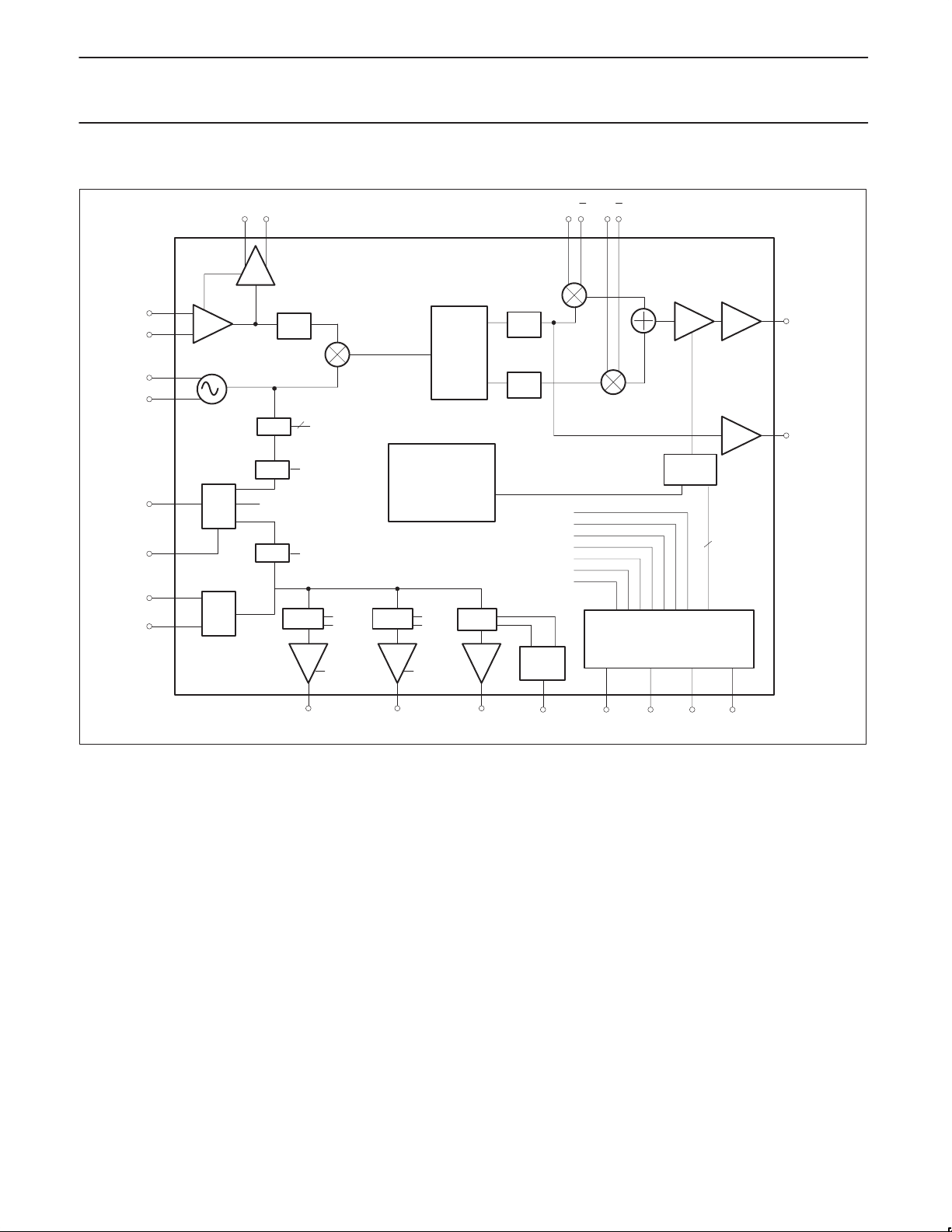
BLOCK DIAGRAM
TXLO_2
TXLO_1
TANK_1
TANK_2
PHSOUT
I
PEAK
XTAL_1
XTAL_2
LO_2 LO_1
VCO
÷N
÷A8/1
PHS
DET
XTAL
OSC
AD
÷B8/1
TXLO
LPF
IMAGE
REJECT
VCO
MIXER
2
AD
AD
÷÷÷
SM1 SM2
SM1 SM2
XY
3/1 4/5/1
2/1
PHASE
SHIFT
NETWORK
BIAS
LPF
LPF
BG
CONV2
II QQ
SE
N<0:1>
AD
SM1
SM2
Y
X
VGA PA
VGA
CONTROL
CONTROL
LOGIC
DUALTX
PA
6
AMPSTX
CLK2CLK1
MCLK
Figure 2. Block Diagram
TXENSTROBECLOCKDATACLKSET
SR00637
1997 Sept 16
3

Philips Semiconductors Preliminary specification
SA900I/Q transmit modulator
PIN DESCRIPTIONS
Pin Description
I Non-inverting I Mod Signal
I Inverting I Mod Signal
TXLO_1/2 Second LO Input (differential/single-ended input)
DUALTX RF output (850MHz) digital (DUAL) mode, complex modulated output
Q Non-inverting Q Mod Signal
Q Inverting Q Mod Signal
CLK1 Buffered oscillator output (XO ÷3/÷1)
MCLK Buffered oscillator output (XO ÷4/÷5/÷1)
CLK2 Buffered oscillator output (XO ÷2/÷1)
AMPSTX RF output (850MHz) AMPS mode
V
CC
GND Ground
Data Serial data input
Clock Serial clock input
Strobe Data strobe input
TXEN AMPS and Dual Mode transmit enable
CLKSET Program control pin for MCLK prescaler
XTAL1 Crystal oscillator base input
XTAL2 Crystal oscillator emitter output
PHSOUT Phase comparator charge pump output
TANK_1 VCO differential tank
TANK_2 VCO differential tank
LO_1/2 Buf fered dif ferential TXLO output
I
PEAK
+5VDC power supply
Phase comparator current programming
1997 Sept 16
4

Philips Semiconductors Preliminary specification
SA900I/Q transmit modulator
GND_LO GND GND GND GND GND_CTRL GND GND GND GND GND GND GND
1 4 11 16 18 25 28 30 33 35 37 39 45
GND
VCC_LO VCC_CTRLVCCVCCVCCV
48 5 8 14 27 29 32 36 38 44 26
V
CC
2
V
CC
3
V
CC
6
CC
50Ω
50Ω
V
CC
VCCVCCVCCV
CC
9
1997 Sept 16
V
CC
7
V
CC
V
CC
0.1/6.4 mA
0.1/6.4 mA
12
V
CC
13
SR00638
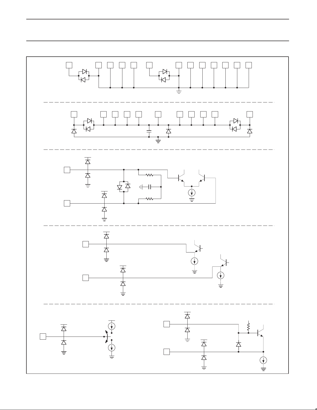
Figure 3. Pin Diagrams
5

Philips Semiconductors Preliminary specification
SA900I/Q transmit modulator
V
CC
19
1715
V
CC
23
2221
V
CC
31
30Ω
24
V
CC
500Ω
20
34
V
CC
500Ω
V
CC
600Ω
42
40
680Ω680Ω
V
CC
43
41
V
CC
47
46
20Ω
SR00639
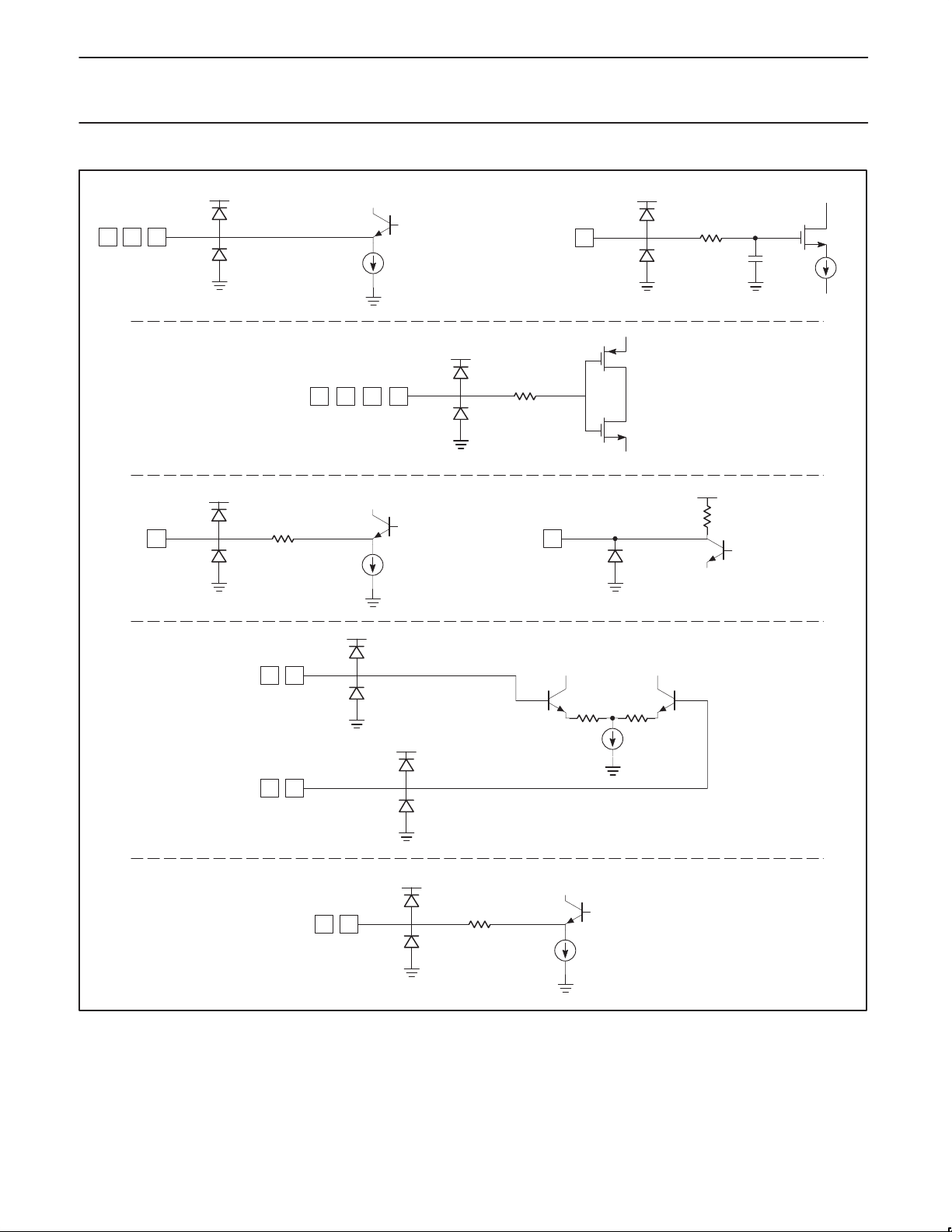
Figure 4. Pin Diagrams (cont.)
1997 Sept 16
6
 Loading...