

Philips sa8026 DATASHEETS

INTEGRATED CIRCUITS
SA8026
2.5GHz low voltage fractional-N
dual frequency synthesizer
Product specification
Supersedes data of 1999 Apr 16
1999 Nov 04

Philips Semiconductors Product specification
TYPE NUMBER
2.5GHz low voltage fractional-N dual frequency
synthesizer
GENERAL DESCRIPTION
The SA8026 BICMOS device integrates programmable dividers,
charge pumps and a phase comparator to implement a
phase-locked loop. The device is designed to operate from 3 NiCd
cells, in pocket phones, with low current and nominal 3 V supplies.
The synthesizer operates at VCO input frequencies up to 2.5 GHz.
The synthesizer has fully programmable main, auxiliary and
reference dividers. All divider ratios are supplied via a 3-wire serial
programming bus.
Separate power and ground pins are provided to the analog and
digital circuits. The ground leads should be externally short-circuited
to prevent large currents flowing across the die and thus causing
damage. V
The charge pump current (gain) is set by an external resistance at
R
pin. Passive loop filters could be used; the charge pump
SET
operates within a wide voltage compliance range to provide a wider
tuning range.
FEA TURES
•Low phase noise
•Low power
•Fully programmable main and auxiliary dividers
•Normal & Integral charge pumps outputs
•Fast Locking Adaptive mode design
•Internal fractional spurious compensation
•Hardware and software power down
•Split supply for V
must be greater than or equal to V
DDCP
and V
DD
DDCP
DD
.
APPLICATIONS
•350 to 2500 MHz wireless equipment
•Cellular phones (all standards)
•WLAN
•Portable battery-powered radio equipment.
LOCK
TEST
RFin+
RFin–
GND
GND
V
GND
PHP
PHI
1
2
3
DD
4
5
6
7
CP
8
9
10
CP
20
19
18
17
16
15
14
13
12
11
PON
STROBE
DATA
CLOCK
REFin+
REFin–
R
V
AUXin
PHA
Figure 1. Pin Configuration
SA8026
SET
DDCP
SR01649
QUICK REFERENCE DATA
ORDERING INFORMATION
SYMBOL PARAMETER CONDITIONS MIN. TYP. MAX. UNIT
V
DD
V
DDCP
I
DDCP+IDD
I
DDCP+IDD
f
VCO
f
AUX
f
REF
f
PC
T
amb
Supply voltage 2.7 – 5.5 V
Analog supply voltage V
DDCP
w
V
DD
2.7 – 5.5 V
Total supply current Main and Aux. on – 10 12 mA
Total supply current in power-down mode – 1 – µA
Input frequency 350 – 2500 MHz
Input frequency 20 – 550 MHz
Crystal reference input frequency 5 – 40 MHz
Maximum phase comparator frequency – 4 MHz
Operating ambient temperature –40 – +85 °C
PACKAGE
NAME DESCRIPTION VERSION
SA8026DH TSSOP20 Plastic thin shrink small outline package; 20 leads; body width 4.4 mm SOT360–1
1999 Nov 04 853–2141 22633
2
Philips Semiconductors Product specification
2.5GHz low voltage fractional-N dual frequency
synthesizer
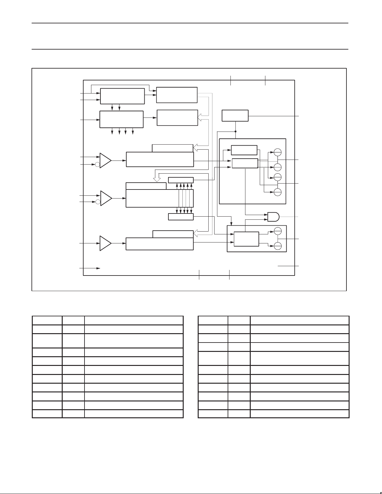
CLOCK
DATA
STROBE
RFin+
RFin–
REFin+
REFin–
17
18
19
5
6
AMP
16
15
2–BIT SHIFT
REGISTER
ADDRESS DECODER
LOAD SIGNALS
LATCH
REFERENCE
DIVIDER
22–BIT SHIFT
REGISTER
LATCH
MAIN DIVIDER
CONTROL
LATCH
SM
2222
SA
V
DD
3
PUMP
CURRENT
SETTING
PUMP
BIAS
COMP
PHASE
DETECTOR
V
DDCP
13
SA8026
14
R
SET
8
PHP
9
PHI
1
LOCK
TEST
12
AMP
2
AUX DIVIDER
AUXin
PINNING
SYMBOL PIN DESCRIPTION
LOCK 1 Lock detect output
TEST 2 Test (should be either grounded or
V
DD
GND 4 Digital ground
RFin+ 5 RF input to main divider
RFin– 6 RF input to main divider
GND
CP
PHP 8 Main normal charge pump
PHI 9 Main integral charge pump
GND
CP
connected to VDD)
3 Digital supply
7 Charge pump ground
10 Charge pump ground
LATCH
4
GND
Figure 2. Block Diagram
SYMBOL PIN DESCRIPTION
PHA 11 Auxiliary charge pump output
AUXin 12 Input to auxiliary divider
V
DDCP
R
SET
REFin– 15 Reference input
REFin+ 16 Reference input
CLOCK 17 Programming bus clock input
DATA 18 Programming bus data input
STROBE 19 Programming bus enable input
PON 20 Power down control
PHASE
DETECTOR
7, 10
GND
CP
11
20
PHA
PON
SR01496
13 Charge pump supply voltage
14 External resistor from this pin to ground
sets the charge pump current
1999 Nov 04
3
Philips Semiconductors Product specification
2.5GHz low voltage fractional-N dual frequency
SA8026
synthesizer
Limiting values
SYMBOL PARAMETER MIN. MAX. UNIT
V
DD
V
DDCP
∆V
DDCP–VDD
V
n
V
n
∆V
GND
T
stg
T
amb
T
j
Handling
Inputs and outputs are protected against electrostatic discharge in normal handling. However, to be totally safe, it is desirable to take normal
precautions appropriate to handling MOS devices.
Digital supply voltage –0.3 +5.5 V
Analog supply voltage –0.3 +5.5 V
Difference in voltage between V
Voltage at pins 1, 2, 5, 6, 12, 15 to 20 –0.3 V
Voltage at pin 8, 9, 11 –0.3 V
Difference in voltage between GNDCP and GND (these pins should be
connected together)
Storage temperature –55 +125
Operating ambient temperature –40 +85
Maximum junction temperature 150
DDCP and
VDD (V
≥ VDD) –0.3 +2.8 V
DDCP
+ 0.3 V
DD
DDCP
–0.3 +0.3 V
+ 0.3 V
_C
_C
_C
Thermal characteristics
SYMBOL PARAMETER VALUE UNIT
R
th j–a
Thermal resistance from junction to ambient in free air 135 K/W
1999 Nov 04
4
Philips Semiconductors Product specification
S
V
AC-coupled input signal level
in
()
S
2.5GHz low voltage fractional-N dual frequency
synthesizer
CHARACTERISTICS
V
DDCP
SYMBOL
= V
= +3.0V, T
DD
PARAMETER CONDITIONS MIN. TYP. MAX. UNIT
Supply; pins 3, 13
V
DD
V
DDCP
I
DDTotal
I
Standby
Digital supply voltage 2.7 – 5.5 V
Analog supply voltage V
Synthesizer operational total supply current V
Total supply current in power-down mode logic levels 0 or VDD – 1 – µΑ
RFin main divider input; pins 5, 6
f
VCO
V
RFin(rms)
Z
IRFin
C
IRFin
N
main
f
PCmax
VCO input frequency 350 – 2500 MHz
AC-coupled input signal level Rin (external) = Rs = 50Ω;
Input impedance (real part) f
Typical pin input capacitance f
Main divider ratio 512 – 65535
Maximum loop comparison frequency indicative, not tested – – 4 MHz
AUX reference divider input; pin 12
f
AUXin
AUXin
Z
AUXin
C
AUXin
N
AUX
Input frequency range 20 – 550 MHz
Input impedance (real part) f
Typical pin input capacitance f
Auxiliary division ratio 128 – 16383
Reference divider input; pins 15, 16
f
REFin
V
RFin
Z
REFin
C
REFin
R
REF
Input frequency range from TCXO 5 – 40 MHz
AC-coupled input signal level single-ended drive;
Input impedance (real part) f
Typical pin input capacitance f
Reference division ratio SA = SM = ”000” 4 – 1023
Charge pump current setting resistor input; pin 14
R
SET
V
SET
External resistor from pin to ground 6 7.5 15 kΩ
Regulated voltage at pin R
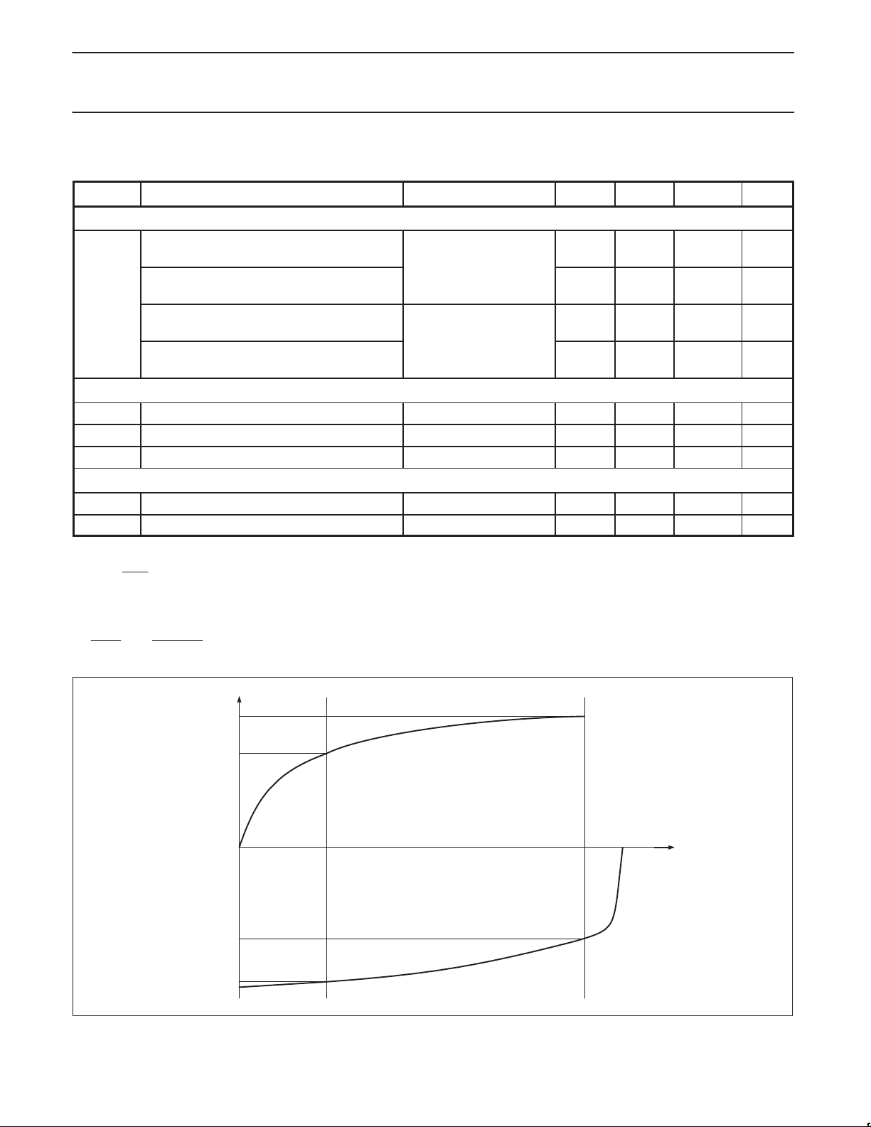
Charge pump outputs (including fractional compensation pump); pins 8, 9, 11; R
I
CP
I
MATCH
I
ZOUT
I
LPH
V
PH
Charge pump current ratio to I
Sink-to-source current matching VPH = 1/2 V
Output current variation versus V
Charge pump off leakage current VPH = 1/2 V
Charge pump voltage compliance 0.7 – V
= +25°C; unless otherwise specified.
amb
p
p
1
SET
PH
V
w
DDCP
DD
(with main and aux on)
DD
= +3.0V
single-ended drive;
max. limit is indicative
@ 500 to 2500 MHz
= 2.4 GHz – 300 – Ω
VCO
= 2.4 GHz – 1 – pF
VCO
Rin (external) = R
max. limit is indicative
= 500 MHz – 3.9 – kΩ
VCO
= 500 MHz – 0.5 – pF
VCO
max. limit is indicative
= 20 MHz – 10 – kΩ
REF
= 20 MHz – 1 – pF
REF
= 7.5 kΩ – 1.25 – V
SET
Current gain = IPH/I
DDCP
2
V
in compliance range –10 +10 %
PH
DDCP
= 50Ω;
= 7.5 kΩ, FC = 80
SET
SET
SA8026
2.7 – 5.5 V
– 10 12 mA
–18 – 0 dBm
–18 – 0 dBm
80 – 632 mV
360 – 1300 mV
–15 +15 %
–10 +10 %
–10 +10 nA
–0.8 V
DDCP
PP
PP
1999 Nov 04
5
Philips Semiconductors Product specification
f
REF
13MHz, TCXO
L
f
REF
44MHz, TCXO
2.5GHz low voltage fractional-N dual frequency
SA8026
synthesizer
CHARACTERISTICS (continued)
SYMBOL PARAMETER CONDITIONS MIN. TYP. MAX. UNIT
Phase noise (condition R
Synthesizer’s contribution to close-in phase noise
of 900 MHz RF signal at 1 kHz offset.
Synthesizer’s contribution to close-in phase noise
of 1800 MHz RF signal at 1 kHz offset.
(f)
Synthesizer’s contribution to close-in phase noise
of 800 MHz RF signal at 1 kHz offset.
Synthesizer’s contribution to close-in phase noise
of 2100 MHz RF signal at 1 kHz offset.
Interface logic input signal levels; pins 2, 17, 18, 19, 20
V
IH
V
IL
I
LEAK
HIGH level input voltage 0.7*V
LOW level input voltage –0.3 – 0.3*V
Input leakage current logic 1 or logic 0 –0.5 – +0.5 µA
Lock detect output signal (in push/pull mode); pin 1
V
OL
V
OH
LOW level output voltage I
HIGH level output voltage I
NOTES:
V
SET
1. I
SET =
bias current for charge pumps.
R
SET
2. The relative output current variation is defined as:
= 7.5 kΩ, CP = 00)
SET
– –90 – dBc/Hz
– –83 – dBc/Hz
f
COMP
=
=
= 1MHz
GSM
,
indicative, not tested
– –85 – dBc/Hz
– –77 – dBc/Hz
f
COMP
=
= 19.
= 240kHz
TDMA
,
indicative, not tested
DD
= 2mA – – 0.4 V
sink
= –2mA VDD–0.4 – – V
source
– VDD+0.3 V
DD
V
DI
OUT
I
OUT
+ 2
.
I(I
(I2–I1)
) I1)I
2
I
ZOUT
; with V1+ 0.7V, V2+ V
CURRENT
I
2
I
1
I
2
I
1
–0.8V (See Figure 3.)
DDCP
V
1
V
V
2
PH
SR00602
Figure 3. Relative Output Current Variation
1999 Nov 04
6
 Loading...