

Philips sa8025a DATASHEETS

SA8025A
Low-voltage 1.8GHz fractional-N
synthesizer
Product specification 1996 Oct 15
INTEGRATED CIRCUITS
IC17 Data Handbook
Philips Semiconductors Product specification
SA8025A1.8GHz low-voltage Fractional-N synthesizer
2
1996 Oct 15 853-1785 17401
DESCRIPTION
The SA8025A is a monolithic low power, high performance dual
frequency synthesizer fabricated in QUBiC BiCMOS technology.
The SA8025A is an improved version of the SA8025, suitable for
narrow band systems like the Japan Personal Digital Cellular (PDC)
system. The new design improves the performance of the fractional
spur compensation circuitry. The new version is pin-for-pin
compatible with the previous version. Featuring Fractional-N
division with selectable modulo 5 or 8 implemented in the Main
synthesizer to allow the phase detector comparison frequency to be
five or eight times the channel spacing. This feature reduces the
overall division ratio yielding a lower noise floor and faster channel
switching. The phase detectors and charge pumps are designed to
achieve phase detector comparison frequencies up to 5MHz. A four
modulus prescaler (divide by 64/65/68/73) is integrated on chip with
a maximum input frequency of 1.8GHz at 3V . Programming and
channel selection are realized by a high speed 3-wire serial
interface. A 1GHz version (SA7025DK) is also available with the
same pinout.
FEATURES
•Operation up to 1.8GHz at 3V
•Fast locking by “Fractional-N” divider
•Auxiliary synthesizer
•Digital phase comparator with proportional and integral charge
pump output
•High speed serial input
•Low power consumption
•Programmable charge pump currents
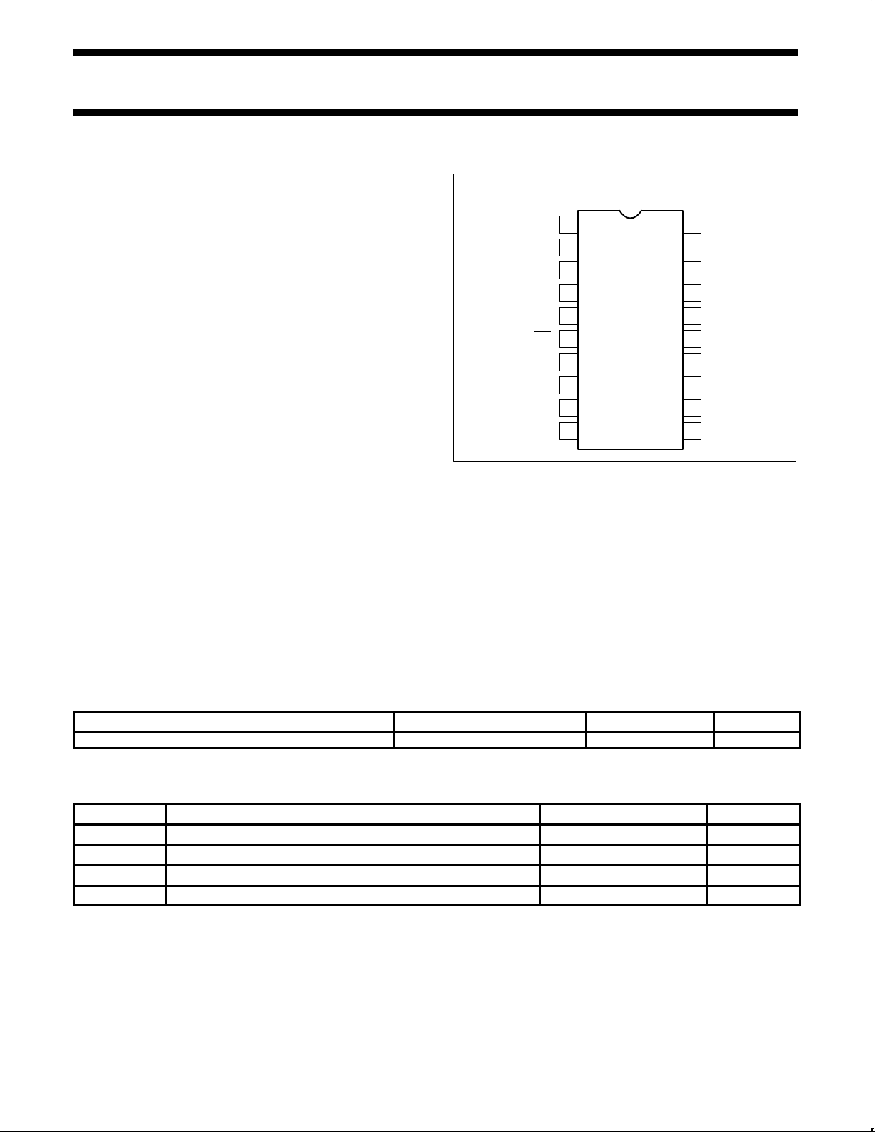
PIN CONFIGURATION
V
SS
DATA
CLOCK
DK Package
1
2
3
4
5
6
7
8
9
10
11
12
13
14
20
19
18
17
16
15
STROBE
RA
TEST
V
DD
RF
RN
PHA
V
DDA
PHP
V
SSA
PHI
LOCK
RF
IN
RF
IN
V
CCP
REF
IN
AUX
IN
SR00623
Figure 1. Pin Configuration
•Supply voltage range 2.7 to 5.5V
•Excellent input sensitivity: V
RF_IN
= –20dBm
APPLICATIONS
•PHS (Personal Handy-phone System)
•PDC (Personal Digital Cellular)
•PCS (Personal Communication Service)
•Portable communication systems
ORDERING INFORMATION
DESCRIPTION TEMPERATURE RANGE ORDER CODE DWG #
20-Pin Plastic Shrink Small Outline Package (SSOP) –40 to +85°C SA8025ADK SOT266-1
ABSOLUTE MAXIMUM RATINGS
SYMBOL PARAMETER RATING UNITS
V Supply voltage, VDD, V
DDA
, V
CCP
-0.3 to +6.0 V
V
IN
Voltage applied to any other pin -0.3 to (VDD + 0.3) V
T
STG
Storage temperature range -65 to +150 °C
T
A
Operating ambient temperature range -40 to +85 °C
NOTE: Thermal impedance (θJA) = 117°C/W. This device is ESD sensitive.
Philips Semiconductors Product specification
SA8025A1.8GHz low-voltage Fractional-N synthesizer
1996 Oct 15
3
PIN DESCRIPTIONS
Symbol Pin Description
CLOCK 1 Serial clock input
DATA 2 Serial data input
STROBE 3 Serial strobe input
V
SS
4 Digital ground
RF
IN
5 Prescaler positive input
RF
IN
6 Prescaler negative input
V
CCP
7 Prescaler positive supply voltage. This pin supplies power to the prescaler and RF input buffer
REF
IN
8 Reference divider input
RA 9 Auxiliary current setting; resistor to V
SSA
AUX
IN
10 Auxiliary divider input
PHA 11 Auxiliary phase detector output
V
SSA
12 Analog ground
PHI 13 Integral phase detector output
PHP 14 Proportional phase detector output
V
DDA
15 Analog supply voltage. This pin supplies power to the charge pumps, Auxiliary prescaler, Auxiliary and Reference
buffers.
RN 16 Main current setting; resistor to V
SSA
RF 17 Fractional compensation current setting; resistor to V
SSA
LOCK 18 Lock detector output
TEST 19 Test pin; connect to V
DD
V
DD
20 Digital supply voltage. This pin supplies power to the CMOS digital part of the device
Philips Semiconductors Product specification
SA8025A1.8GHz low-voltage Fractional-N synthesizer
1996 Oct 15
4
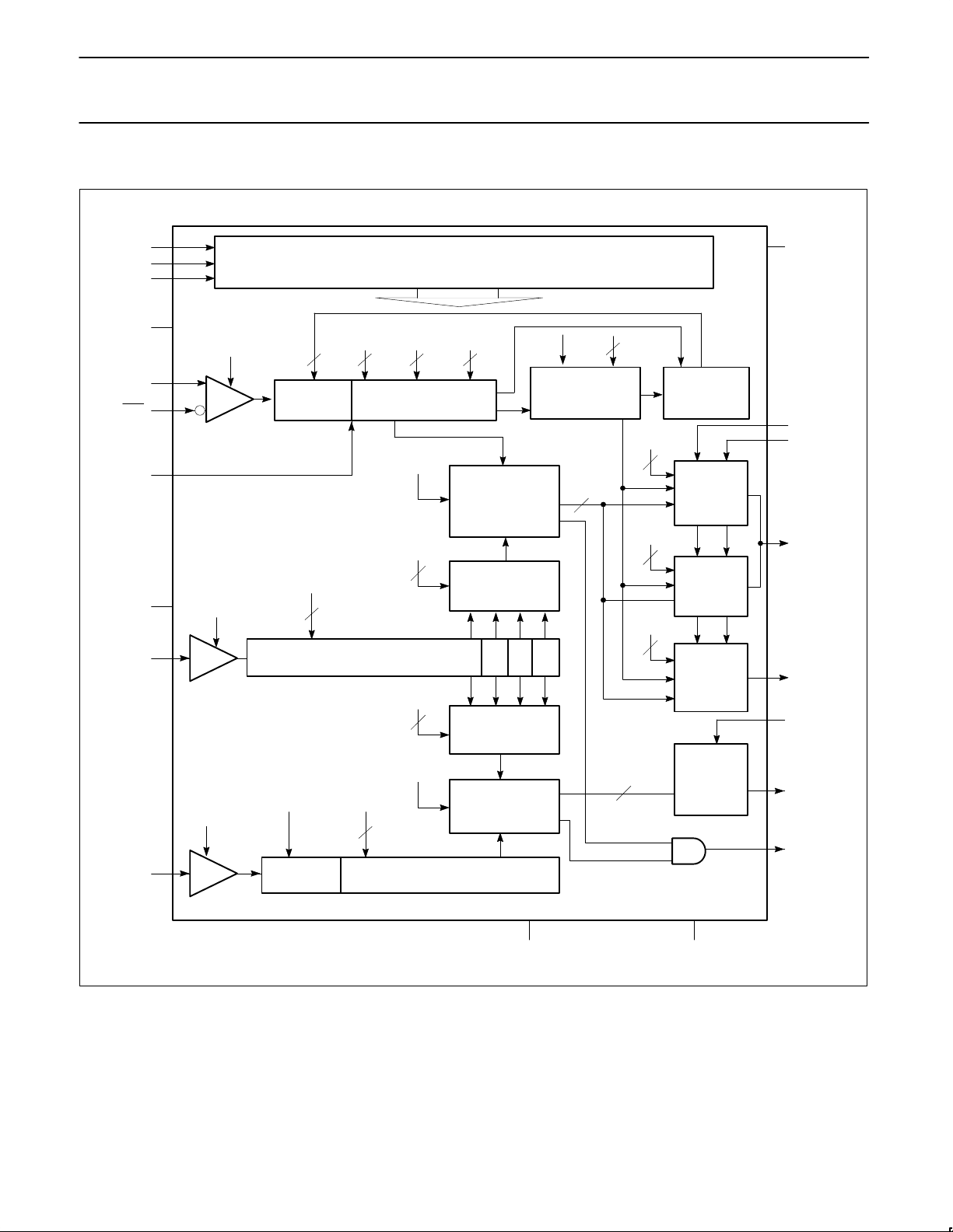
BLOCK DIAGRAM
SERIAL INPUT + PROGRAM LATCHES
MAIN DIVIDERS
PRESCALER
MODULUS
NORMAL
OUTPUT
CHARGE
PUMP
INTEGRAL
OUTPUT
CHARGE
PUMP
AUXILIARY
OUTPUT
CHARGE
PUMP
MAIN
PHASE
DETECTOR
MAIN
REFERENCE
SELECT
SPEED-UP
OUTPUT
CHARGE
PUMP
REFERENCE DIVIDER ÷2 ÷2 ÷2
AUXILIARY
REFERENCE
SELECT
AUXILIARY
PHASE
DETECTOR
AUXILIARY DIVIDER
1/4
DATA
CLOCK
STROBE
RF
IN
RF
IN
REF
IN
AUX
IN
FB
RF
RN
PHP
PHI
RA
PHA
LOCK
V
DD
V
DDA
V
SS
V
SSA
EM
PR NM1
NM2
NM3
FMOD
NF
2
12 8
3
FRD
CN
8
2
2
EM
NR
EM+EA
12
SA
EA
PA NA
2
4
SM
EA
2
CK
CL
2
12
FRACTIONAL
ACCUMULATOR
64/65/68/73
FB
TEST
V
CCP
PRESCALER
2
CONTROL
PRESCALER
SR00624
Figure 2. Block Diagram
Philips Semiconductors Product specification
SA8025A1.8GHz low-voltage Fractional-N synthesizer
1996 Oct 15
5
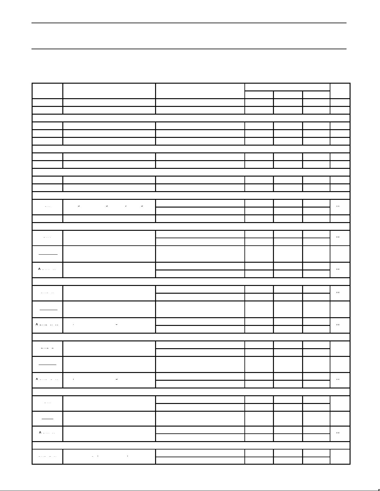
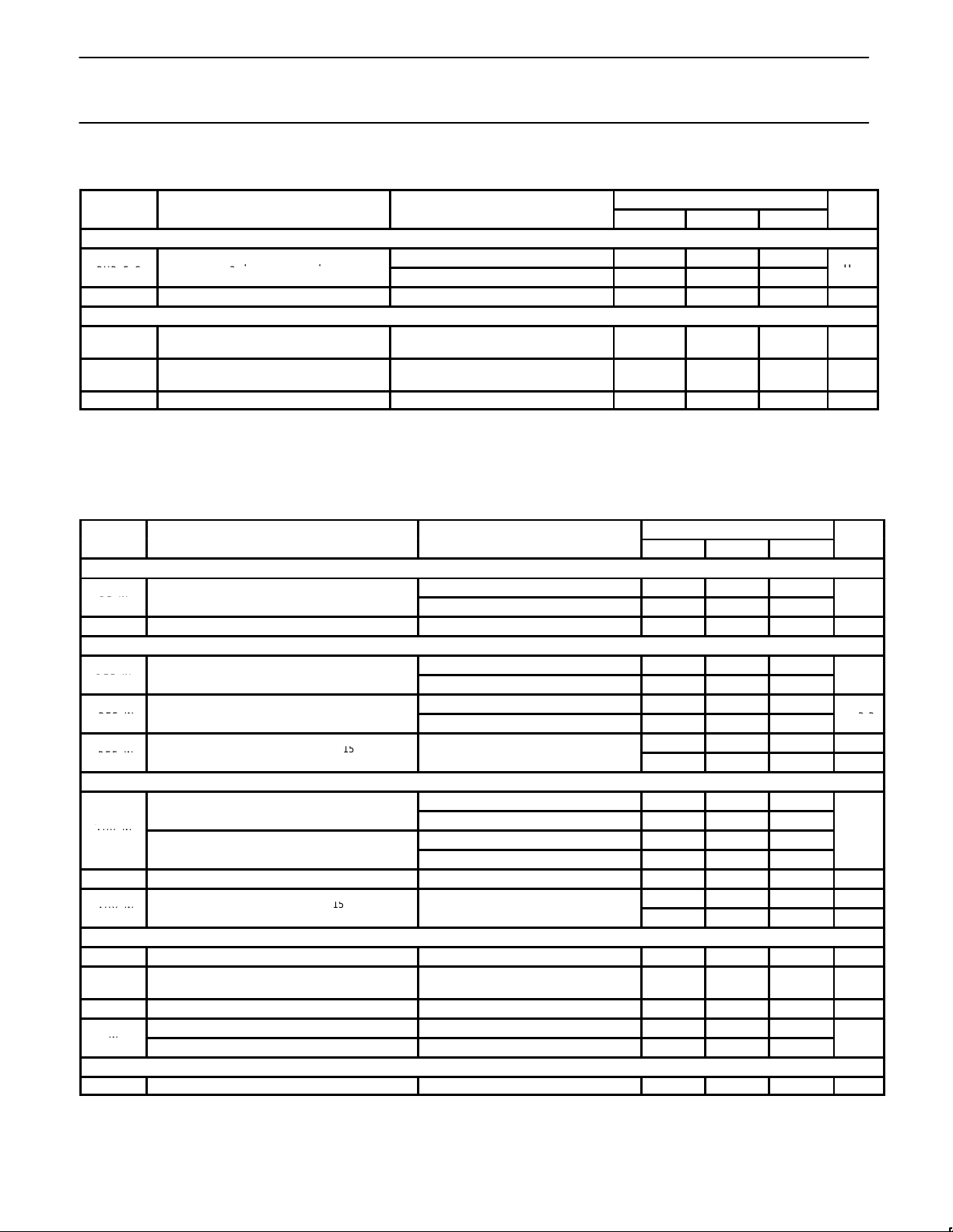
DC ELECTRICAL CHARACTERISTICS
VDD = V
DDA
= V
CCP
= 3V; TA = 25°C, unless otherwise specified.
LIMITS
SYMBOL
PARAMETER
TEST CONDITIONS
MIN TYP MAX
UNITS
V
SUPPLY
Recommended operating conditions V
CCP
= VDD, V
DDA
≥ V
DD
2.7 5.5 V
I
STANDBY
Total standby supply currents EM = EA = 0, IRN = IRF = IRA = 0 50 500 µA
Operational supply currents: I = IDD + I
CCP
+ I
DDA
; IRN = 25µA, IRA = 25µA, (see Note 5)
I
AUX
Operational supply currents EM = 0, EA = 1 3.5 mA
I
MAIN
Operational supply currents EM = 1, EA = 0 11.0 mA
I
TOTAL
Operational supply currents EM = EA = 1 13.5 mA
Digital inputs CLK, DATA, STROBE
V
IH
High level input voltage range 0.7xV
DD
V
DD
V
V
IL
Low level input voltage range 0 0.3xV
DD
V
Digital outputs LOCK
V
OL
Output voltage LOW IO = 2mA 0.4 V
V
OH
Output voltage HIGH IO = –2mA VDD–0.4 V
Charge pumps: V
DDA
= 3V / IRX = 25µA or V
DDA
= 5V / IRX = 62.5µA, V
PHX
in range, unless otherwise specified.
2.7V < V
DDA
< 5.5V 25
|IRX|
Setting current range for any setting re-
sistor
4.5V < V
DDA
< 5.5V 62.5
µA
V
PHOUT
Output voltage range 0.7 V
DDA
–0.8 V
Charge pump PHA
IRN = –62.5µA; V
PHP
= V
DDA
/2
13
400 500 600
|I
PHA
|
Output current PHA
IRN = –25µA; V
PHP
= V
DDA
/2 160 200 240
µA
I
PHP_A
| I
PHP_A
|
Relative output current variation PHA IRA = –62.5µA
2, 13
2 6 %
V
DDA
= 3V, IRA = 25µA ±50
∆I
PHA_M
Output current matching PHA pump
V
DDA
= 5V, IRA = 62.5µA ±65
µA
Charge pump PHP, normal mode
NO TAG, 4, 6
VRF = V
DDA
IRN = –62.5µA; V
PHP
= V
DDA
/2
13
440 550 660
|I
PHP_N
|
Output current PHP
IRN = –25µA; V
PHP
= V
DDA
/2 175 220 265
µA
I
PHP_N
I
PHP_N
Relative output current variation PHP IRN = –62.5µA
2, 13
2 6 %
V
DDA
= 3V, IRA = 25µA ±50
∆I
PHP_N_M
Output current matching PHP
normal mode
V
DDA
= 5V, IRA = 62.5µA ±65
µA
Charge pump PHP, speed-up mode
NO TAG, 4, 7
VRF = V
DDA
IRN = –62.5µA; V
PHP
= V
DDA
/2
13
2.20 2.75 3.30
|I
PHP_S
|
Output current PHP
IRN = –25µA; V
PHP
= V
DDA
/2 0.85 1.1 1.35
mA
I
PHP_S
I
PHP_S
Relative output current variation PHP IRN = –62.5µA
2, 13
2 6 %
V
DDA
= 3V, IRA = 25µA ±250
∆I
PHP_S_M
Output current matching PHP
speed-up mode
V
DDA
= 5V, IRA = 62.5µA ±300
µA
Charge pump PHI, speed-up mode
NO TAG, 4, 8
VRF = V
DDA
IRN = –62.5µA; V
PHI
= V
DDA
/2
13
4.4 5.5 6.6
|I
PHI
|
Output current PHI
IRN = –25µA; V
PHI
= V
DDA
/2 1.75 2.2 2.65
mA
I
PHI
I
PHI
Relative output current variation PHI IRN = –62.5µA
2, 13
2 8 %
V
DDA
= 3V, IRA = 25µA ±500
∆I
PHI_M
Output current matching PHI pump
V
DDA
= 5V, IRA = 62.5µA ±600
µA
Fractional compensation PHP, normal mode
NO TAG, 9
V
RN
= V
DDA
, V
PHP
= V
DDA
/2
IRF = –62.5µA;FRD = 1 to 7
13
–625 –400 –250
I
PHP_F_N
Fractional compensation output current
PHP vs F
RD
3
IRF = –25µA;FRD = 1 to 7 –300 –180 –50
nA
Setting current range for any setting re-
Output current matching PHP
Output current matching PHP
Fractional compensation output current
Philips Semiconductors Product specification
SA8025A1.8GHz low-voltage Fractional-N synthesizer
1996 Oct 15
6
DC ELECTRICAL CHARACTERISTICS (Continued)
LIMITS
SYMBOL
PARAMETER
TEST CONDITIONS
MIN TYP MAX
UNITS
Fractional compensation PHP, speed up mode
NO TAG, 10
V
PHP
= V
DDA
, VRN = V
DDA
IRF = –62.5µA;FRD = 1 to 7
13
–3.35 –2 –1.1
I
PHP_F_S
Fractional compensation output current
PHP vs F
RD
3
IRF = –25µA;FRD = 1 to 7 –1.35 –1.0 –0.5
µA
Pump leakage –20 20 nA
Charge pump leakage currents, charge pump not active
I
PHP_L
Output leakage current PHP; normal
mode
NO TAG
V
PHP
= 0.7 to V
DDA
– 0.8 0.1 20 nA
I
PHI_L
Output leakage current PHI; normal
mode
NO TAG
V
PHI
= 0.7 to V
DDA
– 0.8 0.1 20 nA
I
PHA_L
Output leakage current PHA V
PHA
= 0.7 to V
DDA
– 0.8 0.1 20 nA
AC ELECTRICAL CHARACTERISTICS
VDD = V
DDA
= V
CCP
= 3V; TA = 25°C; unless otherwise specified. Test Circuit, Figure 4. The parameters listed below are tested using
automatic test equipment to assure consistent electrical characteristics. The limits do not represent the ultimate performance limits of the
device. Use of an optimized RF layout will improve many of the listed parameters.
LIMITS
SYMBOL
PARAMETER
TEST CONDITIONS
MIN TYP MAX
UNITS
Main divider guaranteed and tested on an automatic tester. Some performance parameters may be improved by using optimized layout.
Pin = -20dBm, Direct coupled input
14
0 1.8
f
RF_IN
Input signal frequency
Pin = -20dBm, 1000pF input coupling 1.8
GHz
V
RF_IN
Input sensitivity fIN = 1800MHz –20 0 dBm
Reference divider (VDD = V
DDA
= 3V or VDD = 3V / V
DDA
= 5V)
2.7 < VDD and V
DDA
< 5.5V 25
f
REF_IN
Input signal frequency
2.7 < VDD and V
DDA
< 4.5V 30
MHz
2.7 < VDD and V
DDA
< 5.5V 500
V
REF_IN
Input signal range, AC coupled
2.7 < VDD and V
DDA
< 4.5V 300
mV
P-P
100 kΩ
Z
REF_IN
Reference divider input impedance
15
3 pF
Auxiliary divider
Input signal frequency 0 50
PA = “0”, prescaler enabled 4.5V ≤ V
DDA
≤ 5.5V 0 150
f
AUX_IN
Input signal frequency 0 30
MHz
PA = “1”, prescaler disabled 4.5V ≤ V
DDA
≤ 5.5V 0 40
V
AUX_IN
Input signal range, AC coupled 200 mV
P-P
100 kΩ
Z
AUX_IN
Auxiliary divider input impedance
15
3 pF
Serial interface
15
f
CLOCK
Clock frequency 10 MHz
t
SU
Set-up time: DATA to CLOCK,
CLOCK to STROBE
30 ns
t
H
Hold time; CLOCK to DATA 30 ns
Pulse width; CLOCK 30
t
W
Pulse width; STROBE B, C, D, E words 30
ns
In-Loop Performance16 V
DDA
= 5V, VDD = 2.7V
RF
MM
Main loop residual FM F
VCO
= 1780MHz 600 900 Hz
Fractional compensation output current
Philips Semiconductors Product specification
SA8025A1.8GHz low-voltage Fractional-N synthesizer
1996 Oct 15
7
AC ELECTRICAL CHARACTERISTICS (Continued)
LIMITS
SYMBOL
PARAMETER
TEST CONDITIONS
MIN TYP MAX
UNITS
A word, PR = ‘01’
(NM2 65) t
W
A word, PR = ‘10’
1
f
VCO
[(NM2 65) (NM3 1) 68] t
W
A word, PR = ‘11’
[(NM2 65 (NM3 1) 68
(NM4 1) 73)] t
W
A word, PR = ‘00’
[(NM2 65) (NM4 1) 73] t
W
NOTES:
1. When a serial input “A” word is programmed, the main charge pumps on PHP and PHI are in the “speed up mode” as long as STROBE = H.
When this is not the case, the main charge pumps are in the “normal mode”.
2. The relative output current variation is defined thus:
I
OUT
I
OUT
2
(I
2
I1)
|(I
2
I1)|
; with V1 = 0.7V, V2 = V
DDA
– 0.8V (see Figure 3).
3. F
RD
is the value of the 3 bit fractional accumulator.
4. Monotonicity is guaranteed with C
N
= 0 to 255.
5. Power supply current measured with f
RF_IN
= 1667.4MHz, NM1 = 0, NM2 = 1, NM3 = 1, NM4 = 4, FMOD = 8, N = 694 6/8, main phase
detector frequency = 2.4MHz, f
REF IN
= 19.2MHz, NR = 8, SM = 1, f
AUX_IN
= 150MHz, NA = 125, SA = 1, PA = 0, auxiliary phase detector
frequency = 300kHz, IRN = IRA = IRF = 25µA, CN = 160, CL = 0, CK = 0, lock condition, normal mode, V
CCP
= VDD = V
DDA
= 3V.
Operational supply current = I
DDA
+ IDD + I
CCP
.
6. Specification condition: CN = 255
7. Specification conditions:
1) CN = 255; CL = 1, or
2) CN = 75; CL = 3
8. Typical output current | I
PHI
| = –IRN x CN x 2
(CL+1)
x CK/32:
1) CN = 160; CL = 3; CK = 1, or
2) CN = 160; CL = 2; CK = 2, or
3) CN = 160; CL = 1; CK = 4, or
4) CN = 160; CL = 0; CK = 8
9. Any RFD, CL = 1 for speed-up pump. The integral pump is intended for switching only and the fractional compensation is not guaranteed.
10.Specification conditions: F
RD
= 1 to 7; CL = 1.
11.Specification conditions:
1) F
RD
= 1 to 7; CL = 1; CK = 2, or
2) F
RD
= 1 to 7; CL = 2; CK = 1.
12.The matching is defined by the sum of the P and the N pump for a given output voltage.
13.Limited analog supply voltage range 4.5 to 5.5V.
14.For f
IN
< 50MHz, low frequency operation requires DC-coupling and a minimum input slew rate of 32V/µs.
15.Guaranteed by design.
16.F
XTAL
= 14.4MHz, V
XTAL
= 500mV
P-P
, comparison Freq. = 200kHz, Loop bandwidth = 5kHz, Audio filter = 300Hz to 15kHz.
t
Pulse width; STROBE
SW
1
f
VCO
1
f
VCO
1
f
VCO
ns
 Loading...