

Philips SA7016 User Manual

INTEGRATED CIRCUITS
SA7016
1.3GHz low voltage fractional-N
synthesizer
Product specification
Supersedes data of 1999 Apr 20
1999 Nov 04

Philips Semiconductors Product specification
TYPE NUMBER
SA70161.3GHz low voltage fractional-N synthesizer
GENERAL DESCRIPTION
The SA7016 BICMOS device integrates programmable dividers,
charge pumps and a phase comparator to implement a
phase-locked loop. The device is designed to operate from 3 NiCd
cells, in pocket phones, with low current and nominal 3 V supplies.
The synthesizer operates at VCO input frequencies up to 1.3 GHz.
The synthesizer has fully programmable main and reference
dividers. All divider ratios are supplied via a 3-wire serial
programming bus.
Separate power and ground pins are provided to the analog and
digital circuits. The ground leads should be externally short-circuited
to prevent large currents flowing across the die and thus causing
damage. V
must be greater than or equal to V
DDCP
DD
.
The charge pump current (gain) is set by an external resistance at
the R
SET pin. Only passive loop filters could be used; the charge
pump operates within a wide voltage compliance range to provide a
wider tuning range.
1
LOCK
2
TEST
3
V
DD
4
GND
5
RFin+
6
RFin–
7
GND
CP
89
PHP
Figure 1. Pin Configuration
PON
16
15
STROBE
14
DATA
13
CLOCK
12
REFin+
11
REFin–
10
R
V
SR01505
SET
DDCP
FEA TURES
•Low phase noise
•Low power
•Fully programmable main divider
APPLICATIONS
•350–1300 MHz wireless equipment
•Cellular phones
•Portable battery-powered radio equipment.
•Internal fractional spurious compensation
•Hardware and software power down
•Split supply for V
QUICK REFERENCE DATA
SYMBOL PARAMETER CONDITIONS MIN. TYP. MAX. UNIT
V
DD
V
DDCP
I
DDCP+IDD
I
DDCP+IDD
f
VCO
f
REF
f
PC
T
amb
and V
DD
DDCP
Supply voltage 2.7 – 5.5 V
Analog supply voltage V
DDCP
≥ V
DD
2.7 – 5.5 V
Total supply current – 6.2 7.3 mA
Total supply current in power-down mode – 1 – µA
Input frequency 350 – 1300 MHz
Crystal reference input frequency 5 – 40 MHz
Maximum phase comparator frequency – 4 MHz
Operating ambient temperature –40 – +85 °C
ORDERING INFORMATION
PACKAGE
NAME DESCRIPTION VERSION
SA7016DH TSSOP16 Plastic thin shrink small outline package; 16 leads; body width 4.4 mm SOT403–1
1999 Nov 04 853–2160 22634
2
Philips Semiconductors Product specification
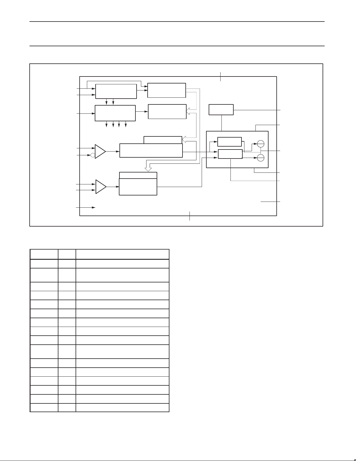
SA70161.3GHz low voltage fractional-N synthesizer
GND
CLOCK
DATA
STROBE
13
14
15
2–BIT SHIFT
REGISTER
ADDRESS DECODER
LOAD SIGNALS
22–BIT SHIFT
REGISTER
CONTROL
LATCH
CURRENT
PUMP
SETTING
PUMP
BIAS
4
10
R
SET
9
V
DDCP
RFin+
RFin–
REF
REF
TEST
5
6
AMP
12
in+
in–
11
2
MAIN DIVIDER
LATCH
REFERENCE
DIVIDER
PINNING
SYMBOL PIN DESCRIPTION
LOCK 1 Lock detect output
TEST 2 Test (should be either grounded or
V
DD
GND 4 Digital ground
RFin+ 5 RF input to main divider
RFin– 6 RF input to main divider
GND
CP
PHP 8 Main normal chargepump
V
DDCP
R
SET
REFin– 11 Reference input
REFin+ 12 Reference input
CLOCK 13 Programming bus clock input
DATA 14 Programming bus data input
STROBE 15 Programming bus enable input
PON 16 Power down control
connected to V
DD)
3 Digital supply
7 Charge pump ground
9 Charge pump supply voltage
10 External resistor from this pin to ground
sets the chargepump current
LATCH
3
V
DD
Figure 2. Block Diagram
COMP
PHASE
DETECTOR
8
PHP
7
GND
1
16
CP
LOCK
PON
SR01506
1999 Nov 04
3

Philips Semiconductors Product specification
SA70161.3GHz low voltage fractional-N synthesizer
LIMITING VALUES
In accordance with the Absolute Maximum Rating System (IEC 134).
SYMBOL PARAMETER MIN. MAX. UNIT
V
DD
V
DDCP
∆V
DDCP–VDD
V
n
V
1
∆V
GND
T
stg
T
amb
T
j
Digital supply voltage –0.3 +5.5 V
Analog supply voltage –0.3 +5.5 V
Difference in voltage between V
DDCP and
Voltage at pins 1, 2, 5, 6, 11 to 16 –0.3 V
Voltage at pin 8, 9 –0.3 V
Difference in voltage between GNDCP and GND (these pins should
VDD (V
≥ VDD) –0.3 +2.8 V
DDCP
+ 0.3 V
DD
DDCP
–0.3 +0.3 V
+ 0.3 V
be connected together)
Storage temperature –55 +125
Operating ambient temperature –40 +85
Maximum junction temperature 150
_C
_C
_C
Handling
Inputs and outputs are protected against electrostatic discharge in
normal handling. However , to be totally safe, it is desirable to take
normal precautions appropriate to handling MOS devices.
THERMAL CHARACTERISTICS
SYMBOL PARAMETER VALUE UNIT
R
th j–a
Thermal resistance from junction to ambient in free air 120 K/W
1999 Nov 04
4

Philips Semiconductors Product specification
SA70161.3GHz low voltage fractional-N synthesizer
CHARACTERISTICS
= V
= +3.0V, T
DD
V
DDCP
SYMBOL
Supply; pins 3, 9
V
DD
V
DDCP
I
DDTotal
I
Standby
Digital supply voltage 2.7 – 5.5 V
Analog supply voltage V
Synthesizer operational total supply current V
Total supply current in power-down mode logic levels 0 or VDD – 1 TBD µA
RFin main divider input; pins 5, 6
f
VCO
V
RFin(rms)
Z
IRFin
C
IRFin
N
main
f
PCmax
VCO input frequency 350 – 1300 MHz
AC-coupled input signal level Rin (external) = Rs = 50Ω;
Input impedance (real part) f
Typical pin input capacitance f
Main divider ratio 512 – 65535
Maximum loop comparison frequency indicative, not tested – – 4 MHz
Reference divider input; pins 11, 12
f
REFin
Input frequency range from TCXO 5 – 40 MHz
VRFin AC-coupled input signal level single-ended drive;
Z
C
R
REFin
REFin
REF
Input impedance (real part) f
Typical pin input capacitance f
Reference division ratio 4 – 1023
Charge pump current setting resistor input; pin 10
R
SET
V
SET
External resistor from pin to ground 6 7.5 15 kΩ
Regulated voltage at pin R
Charge pump outputs (including fractional compensation pump); pin 8; R
I
CP
I
MATCH
I
ZOUT
I
LPH
V
PH
Charge pump current ratio to I
Sink-to-source current matching VPH=1/2 V
Output current variation versus V
Charge pump off leakage current VPH=1/2 V
Charge pump voltage compliance 0.7 – V
= +25°C; unless otherwise specified.
amb
PARAMETER CONDITIONS MIN. TYP. MAX. UNIT
= V
DDCP
DD
DD
= +3.0V – 6.2 7.3 mA
2.7 – 5.5 V
–18 – 0 dBm
single-ended drive;
max. limit is indicative
@ 500 to 1300 MHz
= 1.2 GHz – 625 – Ω
VCO
= 1.2 GHz – 1.0 – pF
VCO
360 – 1300 mV
max. limit is indicative
= 20 MHz – 10 – kΩ
REF
= 20 MHz – 1.0 – pF
REF
=7.5 kΩ – 1.25 – V
SET
=7.5kΩ, FC=80
SET
SET
PH
1
2
Current gain IPH/I
V
in compliance range –10 +10 %
PH
SET
. –10 +10 %
DDCP
CC
–15 +15 %
–10 +10 nA
DDCP
PP
–0.8 V
1999 Nov 04
5

Philips Semiconductors Product specification
L
SA70161.3GHz low voltage fractional-N synthesizer
SYMBOL UNITMAX.TYP.MIN.CONDITIONSPARAMETER
Phase noise (R
(f)
Interface logic input signal levels; pins 13, 14, 15, 16
V
IH
V
IL
I
LEAK
Lock detect output signal (in push/pull mode); pin 1
V
OL
V
OH
NOTES:
V
SET =
SET
R
SET
1. I
2. The relative output current variation is defined as:
DI
OUT
+ 2
I
OUT
= 7.5 kΩ, CP=00)
SET
Synthesizer’s contribution to close-in phase noise
of 900 MHz RF signal at 1 kHz offset.
f
REF
f
COMP
GSM
= 13MHz, TCXO,
= 1MHz
– –90 – dBc/Hz
indicative, not tested
Synthesizer’s contribution to close-in phase noise
of 800 MHz RF signal at 1 kHz offset.
f
REF
f
COMP
TDMA
= 19.44MHz, TCXO,
= 240kHz
– –85 – dBc/Hz
indicative, not tested
HIGH level input voltage 0.7*V
DD
LOW level input voltage –0.3 – 0.3*V
– VDD+0.3 V
DD
Input leakage current logic 1 or logic 0 –0.5 – +0.5 µA
LOW level output voltage I
HIGH level output voltage I
=2mA – – 0.4 V
sink
=–2mA VDD–0.4 – – V
source
bias current for charge pumps.
(I2–I1)
.
I(I
; with V1+ 0.7V, V2+ V
) I1)I
2
–0.8V (See Figure 3.)
DDCP
V
I
ZOUT
CURRENT
I
2
I
1
I
2
I
1
V
1
Figure 3. Relative Output Current Variation
V
V
2
PH
SR00602
1999 Nov 04
6
 Loading...