

Philips SA676DK Datasheet
Philips Semiconductors Product specification
SA676Low-voltage mixer FM IF system
6–129
1993 Dec 15 853-1726 11659
DESCRIPTION
The SA676 is a low-voltage monolithic FM IF system incorporating a
mixer/oscillator, two limiting intermediate frequency amplifiers,
quadrature detector, logarithmic received signal strength indicator
(RSSI), voltage regulator and audio and RSSI op amps. The SA676
is available in a 20-pin SSOP (shrink small outline package).
The SA676 was designed for cordless telephone applications in
which efficient and economic integrated solutions are required and
yet high performance is desirable. Although the product is not
targeted to meet the stringent specifications of high performance
cellular equipment, it will exceed the needs for analog cordless
phones. The minimal amount of external components and absence
of any external adjustments makes for a very economical solution.
FEA TURES
•Low power consumption: 3.5mA typical at 3V
•Mixer input to >100MHz
•Mixer conversion power gain of 17dB at 45MHz
•XTAL oscillator ef fective to 100MHz (L.C. oscillator or external
oscillator can be used at higher frequencies)
•102dB of IF Amp/Limiter gain
•2MHz IF amp/limiter small signal bandwidth
•Temperature compensated logarithmic Received Signal Strength
Indicator (RSSI) with a 70dB dynamic range
•Low external component count; suitable for crystal/ceramic/LC
filters
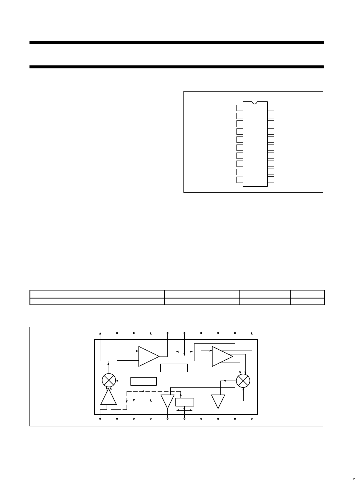
PIN CONFIGURA TION
RF IN+
RF IN– DECOUPLING
OSC
OUT
OSC
IN
RSSI OUT
7
20 MIXER OUT
19
18 IF AMP IN
17
16 IF AMP OUT
15 GND
14 LIMITER IN
13
12
11 LIMITER OUT
V
CC
DK Package
AUDIO FEEDBACK
8
RSSI FEEDBACK
9
QUADRATURE IN 10
IF AMP DECOUPLING
AUDIO OUT
IF AMP DECOUPLING
LIMITER DECOUPLING
LIMITER DECOUPLING
2
1
3
4
5
6
SR00514
Figure 1. Pin Configuration
•Audio output internal op amp
•RSSI output internal op amp
•Internal op amps with rail-to-rail outputs
•ESD protection: Human Body Model 2kV
Robot Model 200V
APPLICA TION
•Cordless phones
ORDERING INFORMATION
DESCRIPTION TEMPERATURE RANGE ORDER CODE DWG #
20-Pin Plastic Shrink Small Outline Package (Surface-mount) -40 to +85°C SA676DK SOT266-1
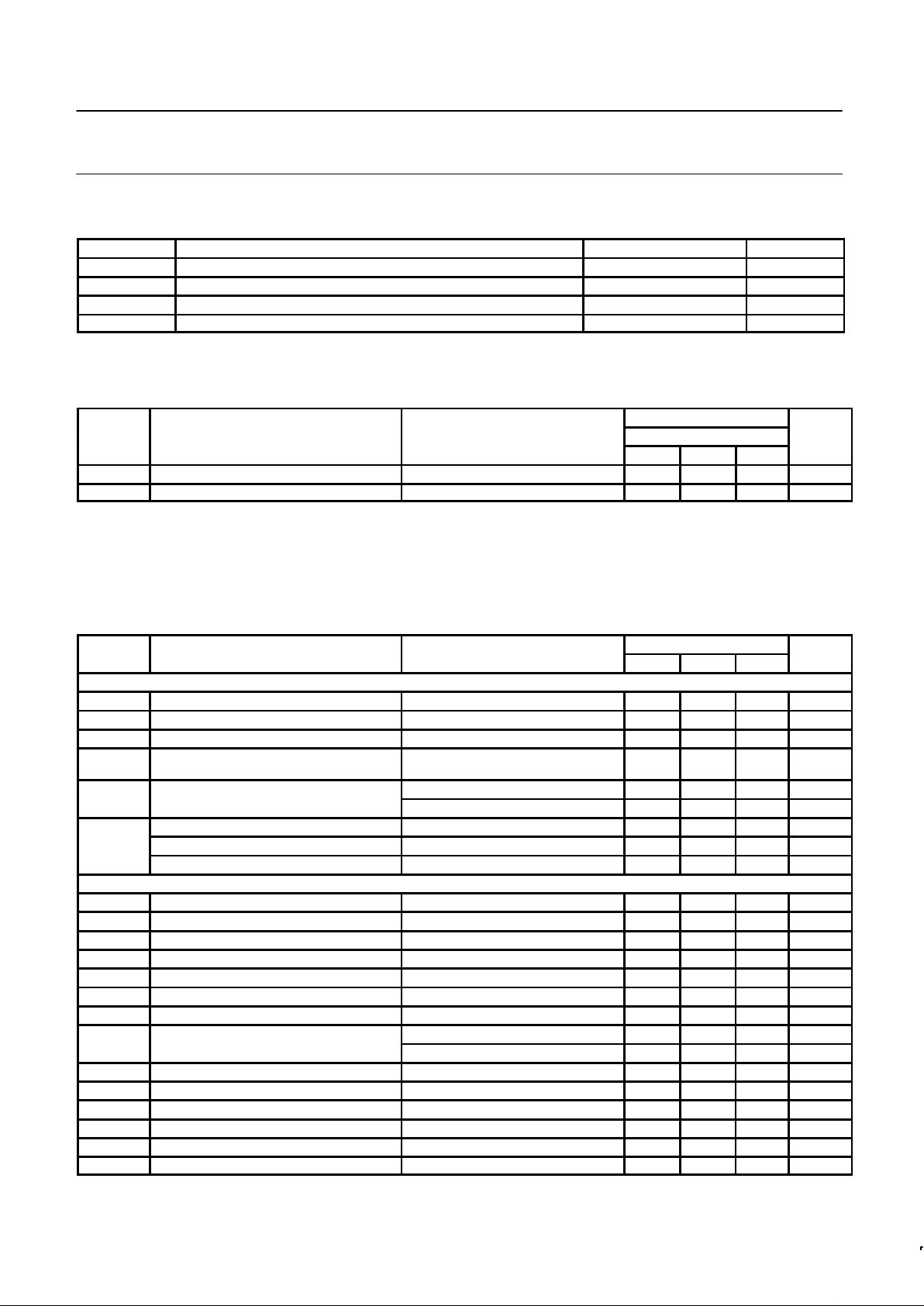
BLOCK DIAGRAM
20 19 18 17 16 15 14 13 12 11
10987654321
RSSI
IF
AMP
EB
V
REG
OSCILLATOR
LIMITER
MIXER
QUAD
+–
+–
AUDIO
SR00515
Figure 2. Block Diagram
Philips Semiconductors Product specification
SA676Low-voltage mixer FM IF system
1993 Dec 15
6–130
ABSOLUTE MAXIMUM RATINGS
SYMBOL PARAMETER RATING UNITS
V
CC
Single supply voltage 7 V
T
STG
Storage temperature range –65 to +150 °C
T
A
Operating ambient temperature range –40 to +85 °C
θ
JA
Thermal impedance DK package 117 °C/W
DC ELECTRICAL CHARACTERISTICS
VCC = +3V, TA = 25°C; unless otherwise stated.
LIMITS
SYMBOL PARAMETER TEST CONDITIONS SA676 UNITS
MIN TYP MAX
V
CC
Power supply voltage range 2.7 7.0 V
I
CC
DC current drain 3.5 5.0 mA
AC ELECTRICAL CHARACTERISTICS
TA = 25°C; VCC = +3V , unless otherwise stated. RF frequency = 45MHz; +14.5dBV RF input step-up; IF frequency = 455kHz; R17 = 2.4kΩ
and R18 = 3.3kΩ; RF level = –45dBm; FM modulation = 1kHz with ±5kHz peak deviation. Audio output with de-emphasis filter and C-message
weighted filter. Test circuit Figure 3. The parameters listed below are tested using automatic test equipment to assure consistent electrical
characteristics. The limits do not represent the ultimate performance limits of the device. Use of an optimized RF layout will improve many of
the listed parameters.
LIMITS
SYMBOL
PARAMETER
TEST CONDITIONS
MIN TYP MAX
UNITS
Mixer/Osc section (ext LO = 220mV
RMS
)
f
IN
Input signal frequency 100 MHz
f
OSC
Crystal oscillator frequency 100 MHz
Noise figure at 45MHz 7.0 dB
Third–order input intercept point (50Ω
source)
f1 = 45.0; f2 = 45.06MHz
Input RF level = –52dBm
–10 dBm
Conversion power gain Matched 14.5dBV step–up 10 17 dB
50Ω source +2.5 dB
RF input resistance Single–ended input 8 kΩ
RF input capacitance 3.0 4.0 pF
Mixer output resistance (Pin 20) 1.25 1.5 kΩ
IF section
IF amp gain 50Ω source 44 dB
Limiter gain 50Ω source 58 dB
AM rejection 30% AM 1kHz 50 dB
Audio level Gain of two 60 120 mV
SINAD sensitivity IF level –110dBm 17 dB
THD T otal harmonic distortion –55 dB
S/N Signal–to–noise ratio No modulation for noise 60 dB
IF RSSI output, R9 = 2kΩ
1
IF level = –110dBm 0.5 .90 V
IF level = –50dBm 1.7 2.2 V
RSSI range 70 dB
IF input impedance Pin 18 1.3 1.5 kΩ
IF output impedance Pin 16 0.3 kΩ
Limiter input impedance Pin 14 1.3 1.5 kΩ
Limiter output impedance Pin 11 0.3 kΩ
Limiter output voltage Pin 11 130 mV
RMS

Philips Semiconductors Product specification
SA676Low-voltage mixer FM IF system
1993 Dec 15
6–131
AC ELECTRICAL CHARACTERISTICS (Continued)
SYMBOL
PARAMETER TEST CONDITIONS LIMITS UNITS
MIN TYP MAX
RF/IF section (int LO)
System SINAD sensitivity RF level = –114dBm 12 dB
NOTE:
1. The generator source impedance is 50Ω, but the SA676 input impedance at Pin 18 is 1500Ω. As a result, IF level refers to the actual signal
that enters the SA676 input (Pin 18) which is about 21dB less than the “available power” at the generator.
CIRCUIT DESCRIPTION
The SA676 is an IF signal processing system suitable for second IF
systems with input frequency as high as 100MHz. The bandwidth of
the IF amplifier and limiter is at least 2MHz with 90dB of gain. The
gain/bandwidth distribution is optimized for 455kHz, 1.5kΩ source
applications. The overall system is well-suited to battery operation
as well as and high quality products of all types.
The input stage is a Gilbert cell mixer with oscillator. Typical mixer
characteristics include a noise figure of 7.0dB, conversion gain of
17dB, and input third-order intercept of –10dBm. The oscillator will
operate in excess of 100MHz in L/C tank configurations. Hartley or
Colpitts circuits can be used up to 100MHz for xtal configurations.
The output impedance of the mixer is a 1.5kΩ resistor permitting
direct connection to a 455kHz ceramic filter. The input resistance of
the limiting IF amplifiers is also 1.5kΩ. With most 455kHz ceramic
filters and many crystal filters, no impedance matching network is
necessary. The IF amplifier has 44dB of gain and 5.5MHz
bandwidth. The IF limiter has 58dB of gain and 4.5MHz bandwidth.
To achieve optimum linearity of the log signal strength indicator,
there must be a 12dB(v) insertion loss between the first and second
IF stages. If the IF filter or interstage network does not cause
12dB(v) insertion loss, a fixed or variable resistor or an L pad for
simultaneous loss and impedance matching can be added between
the first IF output (Pin 16) and the interstage network. The overall
gain will then be 90dB with 2MHz bandwidth.
The signal from the second limiting amplifier goes to a Gilbert cell
quadrature detector . One port of the Gilbert cell is internally driven
by the IF. The other output of the IF is AC-coupled to a tuned
quadrature network. This signal, which now has a 90° phase
relationship to the internal signal, drives the other port of the
multiplier cell.
The demodulated output of the quadrature drives an internal op
amp. This op amp can be configured as a unity gain buffer, or for
simultaneous gain, filtering, and 2nd-order temperature
compensation if needed. It can drive an AC load as low as 10kΩ
with a rail-to-rail output.
A log signal strength indicator completes the circuitry. The output
range is greater than 70dB and is temperature compensated. This
signal drives an internal op amp. The op amp is capable of
rail-to-rail output. It can be used for gain, filtering, or 2nd-order
temperature compensation of the RSSI, if needed.
NOTE: dB(v) = 20log V
OUT/VIN
 Loading...