

Philips SA617DK Datasheet

RF COMMUNICATIONS PRODUCTS
SA617
Low-voltage high performance mixer
FM IF system
Product specification
Replaces data of November 3, 1992
IC17 Data Handbook
Philips Semiconductors
1997 Nov 07
Philips Semiconductors Product specification
SA617Low-voltage high performance mixer FM IF system
DESCRIPTION
The SA617 is a low voltage high performance monolithic FM IF
system incorporating a mixer/oscillator, two limiting intermediate
frequency amplifiers, quadrature detector, logarithmic received
signal strength indicator (RSSI), voltage regulator and audio and
RSSI op amps. The SA617 is available in 20-lead SSOP package.
The SA617 was designed for portable communication applications
and will function down to 2.7V. The RF section is similar to the
famous SA605. The audio output has an internal amplifier with the
feedback pin accessible. The RSSI output is buffered. The SA617
also has an extra limiter output. This signal is buffered from the
output of the limiter and can be used to perform frequency check.
This is accomplished by comparing a reference frequency with the
frequency check signal using a comparator to a varactor or PLL at
the oscillator inputs.
FEA TURES
•Low power consumption: 3.5mA typical at 3V
•Mixer input to >150MHz
•Mixer conversion power gain of 17dB at 45MHz
•XTAL oscillator ef fective to 150MHz (L.C. oscillator or external
oscillator can be used at higher frequencies)
•102dB of IF Amp/Limiter gain
•2MHz IF amp/limiter small signal bandwidth
•Temperature compensated logarithmic Received Signal Strength
Indicator (RSSI) with a 80dB dynamic range
•Low external component count; suitable for crystal/ceramic/LC
filters
•Excellent sensitivity: 0.31µV into 50Ω matching network for 12dB
SINAD (Signal to Noise and Distortion ratio) for 1kHz tone, 8kHz
deviation with RF at 45MHz and IF at 455kHz
•SA617 meets cellular radio specifications
•Audio output internal op amp
•RSSI output internal op amp
•Buffered frequency check output
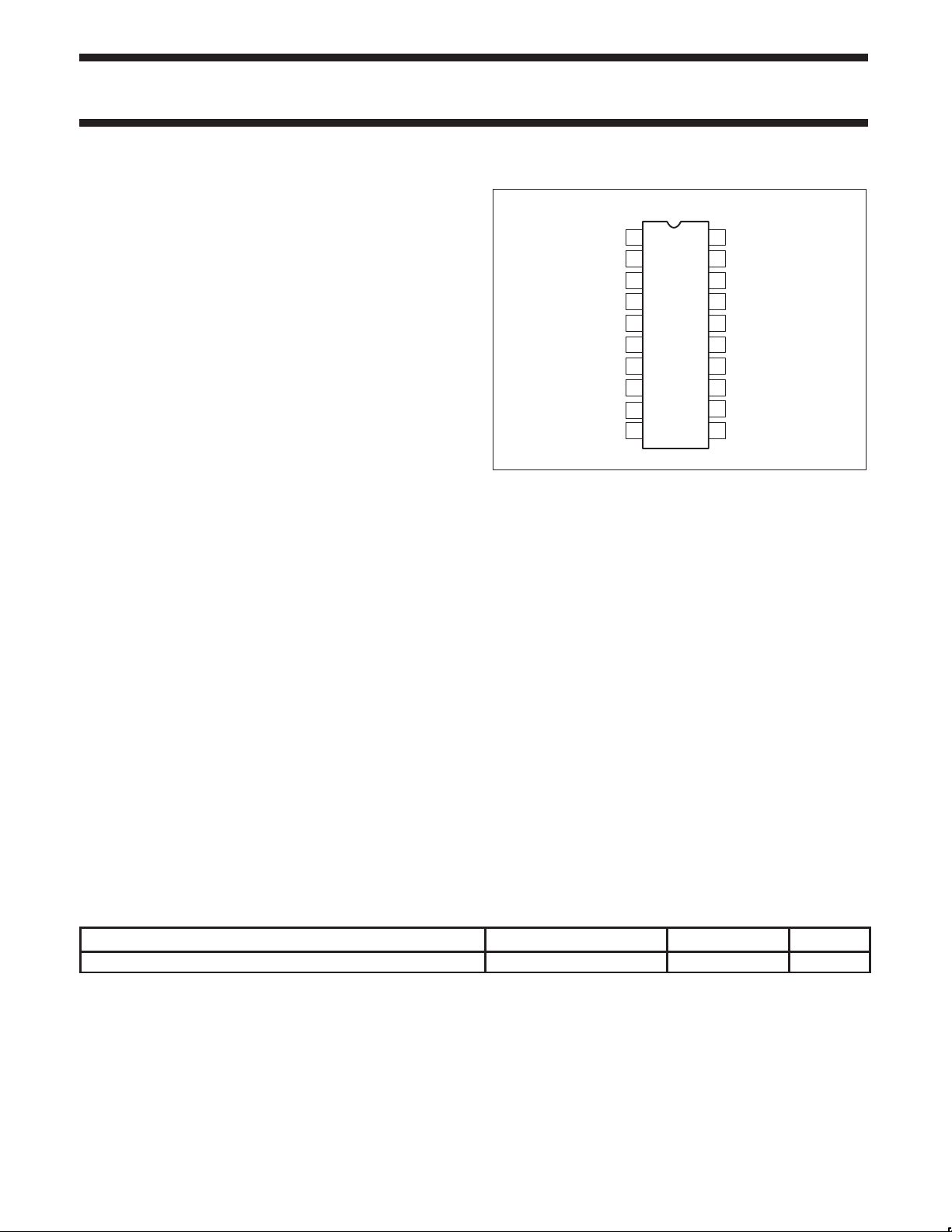
PIN CONFIGURATION
DK Package
1
RF IN+
RF IN– DECOUPLING
OSC
OUT
OSC
IN
RSSI OUT
V
CC
AUDIO FEEDBACK
AUDIO OUT
FREQ CHECK/LIM OUT (–)
QUADRATURE IN
Figure 1. Pin Configuration
2
3
4
5
6
7
8
9
10
20 MIXER OUT
IF AMP DECOUPLING
19
18 IF AMP IN
17
IF AMP DECOUPLING
16 IF AMP OUT
15 GND
14 LIMITER IN
13
LIMITER DECOUPLING
12
LIMITER DECOUPLING
11
LIM OUT (+)
•Internal op amps with rail-to-rail outputs
•ESD protection: Human Body Model 2kV
Robot Model 200V
APPLICA TIONS
•Portable cellular radio FM IF
•Cordless phones
•Narrow band cellular applications (NAMPS/NTACS)
•RF level meter
•Spectrum analyzer
•Instrumentation
•FSK and ASK data receivers
•Log amps
•Portable high performance communication receivers
•Single conversion VHF receivers
•Wireless systems
SR00405
ORDERING INFORMATION
DESCRIPTION TEMPERATURE RANGE ORDER CODE DWG #
20-Pin Plastic Shrink Small Outline Package (SSOP) (Surface-mount) -40 to +85°C SA617DK SOT266-1
1997 Nov 07 853-1678 18665
2
Philips Semiconductors Product specification
SA617Low-voltage high performance mixer FM IF system
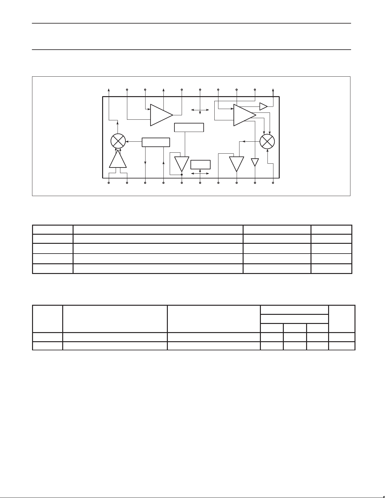
BLOCK DIAGRAM
20 19 18 17 16 15 14 13 12 11
MIXER
IF
AMP
OSCILLATOR
EB
RSSI
+–
V
REG
LIMITER
QUAD
+–
AUDIO
10987654321
SR00406
Figure 2. Block Diagram
ABSOLUTE MAXIMUM RATINGS
SYMBOL PARAMETER RATING UNITS
T
V
θ
CC
STG
T
A
JA
Single supply voltage 7 V
Storage temperature range –65 to +150
Operating ambient temperature range SA617 –40 to +85
Thermal impedance DK package 117
°C/W
°C
°C
DC ELECTRICAL CHARACTERISTICS
VCC = +3V, TA = 25°C; unless otherwise stated.
LIMITS
SYMBOL PARAMETER TEST CONDITIONS SA617 UNITS
MIN TYP MAX
V
CC
I
CC
Power supply voltage range 2.7 7.0 V
DC current drain 3.5 5.0 mA
1997 Nov 07
3
Philips Semiconductors Product specification
SA617Low-voltage high performance mixer FM IF system
AC ELECTRICAL CHARACTERISTICS
TA = 25°C; VCC = +3V, unless otherwise stated. RF frequency = 45MHz + 14.5dBV RF input step-up; IF frequency = 455kHz; R17 = 2.4k; R18
= 3.3k; RF level = –45dBm; FM modulation = 1kHz with ±8kHz peak deviation. Audio output with de-emphasis filter and C-message weighted
filter. Test circuit NO TAG. The parameters listed below are tested using automatic test equipment to assure consistent electrical
characterristics. The limits do not represent the ultimate performance limits of the device. Use of an optimized RF layout will improve many of
the listed parameters.
LIMITS
SYMBOL PARAMETER TEST CONDITIONS SA617 UNITS
MIN TYP MAX
Mixer/Osc section (ext LO = 220mV
f
OSC
f
IN
Input signal frequency 150 MHz
Crystal oscillator frequency 150 MHz
Noise figure at 45MHz 6.8 dB
Third–order input intercept point (50Ω
source)
Conversion power gain Matched 14.5dBV step–up 11.0 17 dB
RF input resistance Single–ended input 8 kΩ
RF input capacitance 3.0 4.0 pF
Mixer output resistance (Pin 20) 1.25 1.5 kΩ
IF section
IF amp gain 50Ω source 44 dB
Limiter gain 50Ω source 58 dB
Input limiting –3dB, R17 = 2.4k Test at Pin 18 –105 dBm
AM rejection 80% AM 1kHz 40 dB
Audio level Gain of two (2kΩ AC load) 60 114 mV
SINAD sensitivity RF level –110dB 13 dB
THD Total harmonic distortion –30 –45 dB
S/N Signal–to–noise ratio No modulation for noise 62 dB
IF RSSI output, R9 = 2kΩ
RSSI range 80 dB
RSSI accuracy +2.0 dB
IF input impedance 1.3 1.5 kΩ
IF output impedance 0.3 kΩ
Limiter input impedance 1.30 1.5 kΩ
Limiter output impedance (Pin 11) 200 Ω
Limiter output level
Frequency Check/limiter output impedance (Pin 9) 200 Ω
Frequency Check/limiter output level
RF/IF section (int LO)
Audio level 3V = VCC, RF level = –27dBm 240 mV
System RSSI output 3V = VCC, RF level = –27dBm 2.2 V
System SINAD sensitivity RF level = –117dBm 12 dB
NOTE:
1. The generator source impedance is 50Ω, but the SA617 input impedance at Pin 18 is 1500Ω. As a result, IF level refers to the actual signal
that enters the SA617 input (Pin 18) which is about 21dB less than the “available power” at the generator.
RMS
1
)
f1 = 45.0; f2 = 45.06MHz
Input RF Level = –52dBm
–9 dBm
50Ω source +2.5 dB
IF level = –118dBm 0.3 0.8 V
IF level = –68dBm .70 1.1 2.0 V
IF level = –23dBm 1.0 1.8 2.5 V
(Pin 11) No load
2.4kΩ load
(Pin 9) No load
2.4kΩ load
130
115
130
115
mV
mV
RMS
RMS
RMS
1997 Nov 07
4

Philips Semiconductors Product specification
SA617Low-voltage high performance mixer FM IF system
CIRCUIT DESCRIPTION
The SA617 is an IF signal processing system suitable for second IF
systems with input frequency as high as 150MHz. The bandwidth of
the IF amplifier and limiter is at least 2MHz with 90dB of gain. The
gain/bandwidth distribution is optimized for 455kHz, 1.5kΩ source
applications. The overall system is well-suited to battery operation
as well as high performance and high quality products of all types.
The input stage is a Gilbert cell mixer with oscillator. Typical mixer
characteristics include a noise figure of 6.2dB, conversion gain of
17dB, and input third-order intercept of –9dBm. The oscillator will
operate in excess of 200MHz in L/C tank configurations. Hartley or
Colpitts circuits can be used up to 100MHz for xtal configurations.
Butler oscillators are recommended for xtal configurations up to
150MHz.
The output impedance of the mixer is a 1.5kΩ resistor permitting
direct connection to a 455kHz ceramic filter. The input resistance of
the limiting IF amplifiers is also 1.5kΩ. With most 455kHz ceramic
filters and many crystal filters, no impedance matching network is
necessary. The IF amplifier has 43dB of gain and 5.5MHz
bandwidth. The IF limiter has 60dB of gain and 4.5MHz bandwidth.
To achieve optimum linearity of the log signal strength indicator,
there must be a 12dB(v) insertion loss between the first and second
IF stages. If the IF filter or interstage network does not cause
12dB(v) insertion loss, a fixed or variable resistor or an L pad for
simultaneous loss and impedance matching can be added between
the first IF output (Pin 16) and the interstage network. The overall
gain will then be 90dB with 2MHz bandwidth.
The signal from the second limiting amplifier goes to a Gilbert cell
quadrature detector . One port of the Gilbert cell is internally driven
by the IF. The other output of the IF is AC-coupled to a tuned
quadrature network. This signal, which now has a 90
relationship to the internal signal, drives the other port of the
multiplier cell.
The demodulated output of the quadrature drives an internal op
amp. This op amp can be configured as a unity gain buffer, or for
simultaneous gain, filtering, and 2nd-order temperature
compensation if needed. It can drive an AC load as low as 2kΩ with
a rail-to-rail output.
A log signal strength completes the circuitry. The output range is
greater than 90dB and is temperature compensated. This log signal
strength indicator exceeds the criteria for AMPs or TACs cellular
telephone. This signal is buffered through an internal unity gain op
amp. The frequency check pin provides a buffered limiter output.
This is useful for implementing an AFC (Automatic Frequency
Check) function. This same output can also be used in conjunction
with limiter output (Pin 11) for demodulating FSK (Frequency Shift
Keying) data. Both pins are of the same amplitude, but 180° out of
phase.
NOTE: Limiter output or Frequency Check output has drive
capability of a load minimum of 2kΩ or higher to obtain 115mV
output level.
NOTE: dB(v) = 20log V
OUT/VIN
° phase
1997 Nov 07
5
Philips Semiconductors Product specification
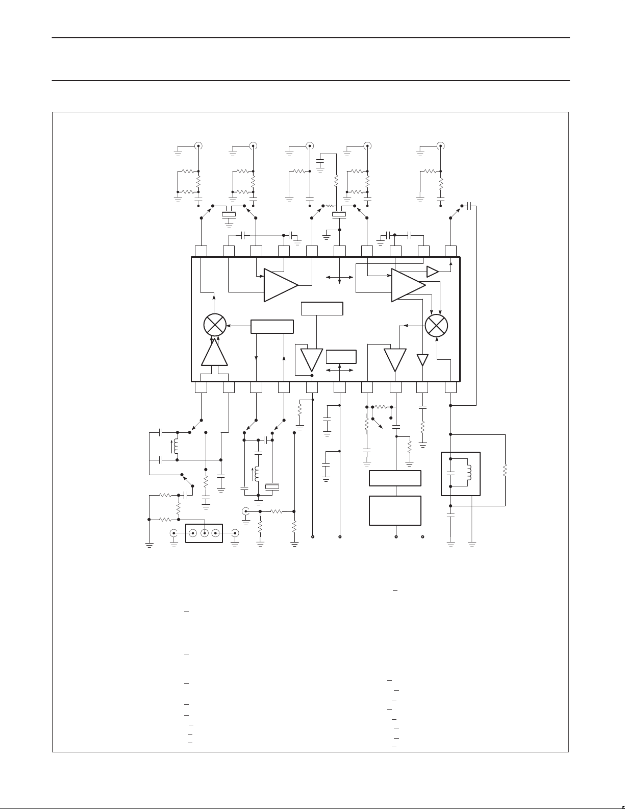
SA617Low-voltage high performance mixer FM IF system
–25dB,
1500/50
Ω PAD
50.5
2430
3880
SW9
20 19 18 17 16 15 14
C1
L1
C2
R4
51.1
SW2
R1
C3
R2
R3
45MHZ
MINI–CIRCUIT ZSC2–1B
–10dB,
50/50
Ω PAD
96.5
71.5
32.6
C24 C22
FLT1
SW8
C23
MIXER
OSCILLATOR
SW3 SW4SW1
C8
C4
C5
EXT.
LOC
OSC
44.545
L2
C6
45.06
MHZ
C7
R6
178
IF
AMP
R7
30.5
–29dB,
929/50
51.5
C21
X1
C20
SW7
R8
39.2
R9
Ω PAD
RSSI
+
–
RSSI
OUT
C26
R18
3.3k
R17
2.4k
C9
C10
V
V
FLT2
REG
CC
–10.6dB,
50/50
Ω PAD
96.5
71.5
32.8
C19
SW6 SW5
C18
–
R11
R10
SW10
C27
C12
DEEMPHASIS
FILTER
”C” WEIGHTED
AUDIO
MEASUREMENT
CIRCUIT
AUDIO
OUT
–36dB,
156k/50
Ω PAD
51.7
1.3k
C16
C17
13 12 11
LIMITER
QUAD
+
AUDIO
10987654321
C26
R17
SW11
R12
C14
C15
IFT1
16k
R19
1997 Nov 07
100pF NPO Ceramic
C1
390pF NPO Ceramic
C2
C5
100nF +
22pF NPO Ceramic
C6
1nF Ceramic
C7
10.0pF NPO Ceramic
C8
C9
100nF +
C10
15
C12
2.2µF
C14
100nF +
10pF NPO Ceramic
C15
C17
100nF +10% Monolithic Ceramic
C18
100nF +
C21
C23
C25
10% Monolithic Ceramic
10% Monolithic Ceramic
µF Tantalum (minimum)
10% Monolithic Ceramic
10% Monolithic Ceramic
10% Monolithic Ceramic
100nF +
100nF +
100nF +
10% Monolithic Ceramic
10% Monolithic Ceramic
Figure 3. SA617 45MHz Test Circuit (Relays as shown)
Automatic Test Circuit Component List
C26
0.1µF +10% Monolithic Ceramic
C27
2.2µF
Flt 1
Ceramic Filter Murata SFG455A3 or equiv
Flt 2
Ceramic Filter Murata SFG455A3 or equiv
IFT 1
455kHz (Ce = 180pF) Toko RMC–2A6597H
L1
147–160nH Coilcraft UNI–10/142–04J08S
L2
X1
R9
R10
R11
R12
R14
R17
R18
R19
µH nominal
3.3
44.545MHz Crystal ICM4712701
2kΩ +
1% 1/4W Metal Film
8.2kΩ +
10kΩ +1%
2kΩ +
1%
10kΩ +
2.4kΩ +
3.3kΩ +
16kΩ +5% 1/4W Carbon Composition
6
Toko 292CNS–T1046Z
1%
1%
5% 1/4W Carbon Composition
5% 1/4W Carbon Composition
SR00407
 Loading...