

Page 1

INTEGRATED CIRCUITS
SA615
High performance low power mixer FM IF
system
Product specification
Replaces data of 1992 Nov 03
IC17 Data Handbook
1997 Nov 07
Page 2

Philips Semiconductors Product specification
SA615High performance low power mixer FM IF system
DESCRIPTION
The SA615 is a high performance monolithic low-power FM IF
system incorporating a mixer/oscillator, two limiting intermediate
frequency amplifiers, quadrature detector, muting, logarithmic
received signal strength indicator (RSSI), and voltage regulator. The
SA615 combines the functions of Signetics’ SA602 and SA604A, but
features a higher mixer input intercept point, higher IF bandwidth
(25MHz) and temperature compensated RSSI and limiters
permitting higher performance application. The SA615 is available in
20-lead dual-in-line plastic, 20-lead SOL (surface-mounted miniature
package) and 20-lead SSOP (shrink small outline package).
The SA605 and SA615 are functionally the same device types. The
difference between the two devices lies in the guaranteed
specifications. The SA615 has a higher I
intercept point, lower conversion mixer gain, lower limiter gain, lower
AM rejection, lower SINAD, higher THD, and higher RSSI error than
the SA615. Both the SA605 and SA615 devices will meet the EIA
specifications for AMPS and TACS cellular radio applications.
For additional technical information please refer to application notes
AN1994, 1995 and 1996, which include example application
diagrams, a complete overview of the product, and artwork for
reference.
, lower input third order
CC
FEATURES
•Low power consumption: 5.7mA typical at 6V
•Mixer input to >500MHz
•Mixer conversion power gain of 13dB at 45MHz
•Mixer noise figure of 4.6dB at 45MHz
•XTAL oscillator effective to 150MHz (L.C. oscillator to 1GHz local
oscillator can be injected)
•102dB of IF Amp/Limiter gain
•25MHz limiter small signal bandwidth
•Temperature compensated logarithmic Received Signal Strength
Indicator (RSSI) with a dynamic range in excess of 90dB
•Two audio outputs – muted and unmuted
•Low external component count; suitable for crystal/ceramic/LC
filters
•Excellent sensitivity: 0.22µV into 50Ω matching network for 12dB
SINAD (Signal to Noise and Distortion ratio) for 1kHz tone with RF
at 45MHz and IF at 455kHz
•SA615 meets cellular radio specifications
•ESD hardened
PIN CONFIGURATION
N, D and DK Packages
RF
1
IN
RF BYPASS
XTAL OSC
XTAL OSC
MUTE
RSSI
MUTED AUDIO OUT
UNMUTED AUDIO OUT
QUADRATURE IN
NOTE:
See back page for package dimensions
2
3
4
5
IN
6
V
CC
7
OUT
8
9
10
Figure 1. Pin Configuration
20
19
18
17
16
15
14
13
12
11
APPLICATIONS
•Cellular radio FM IF
•High performance communications receivers
•Single conversion VHF/UHF receivers
•SCA receivers
•RF level meter
•Spectrum analyzer
•Instrumentation
•FSK and ASK data receivers
•Log amps
•Wideband low current amplification
MIXER OUT
IF AMP DECOUPLING
IF AMP IN
IF AMP DECOUPLING
IF AMP OUT
GND
LIMITER IN
LIMITER DECOUPLING
LIMITER DECOUPLING
LIMITER OUT
SR00341
ORDERING INFORMATION
DESCRIPTION TEMPERATURE RANGE ORDER CODE DWG #
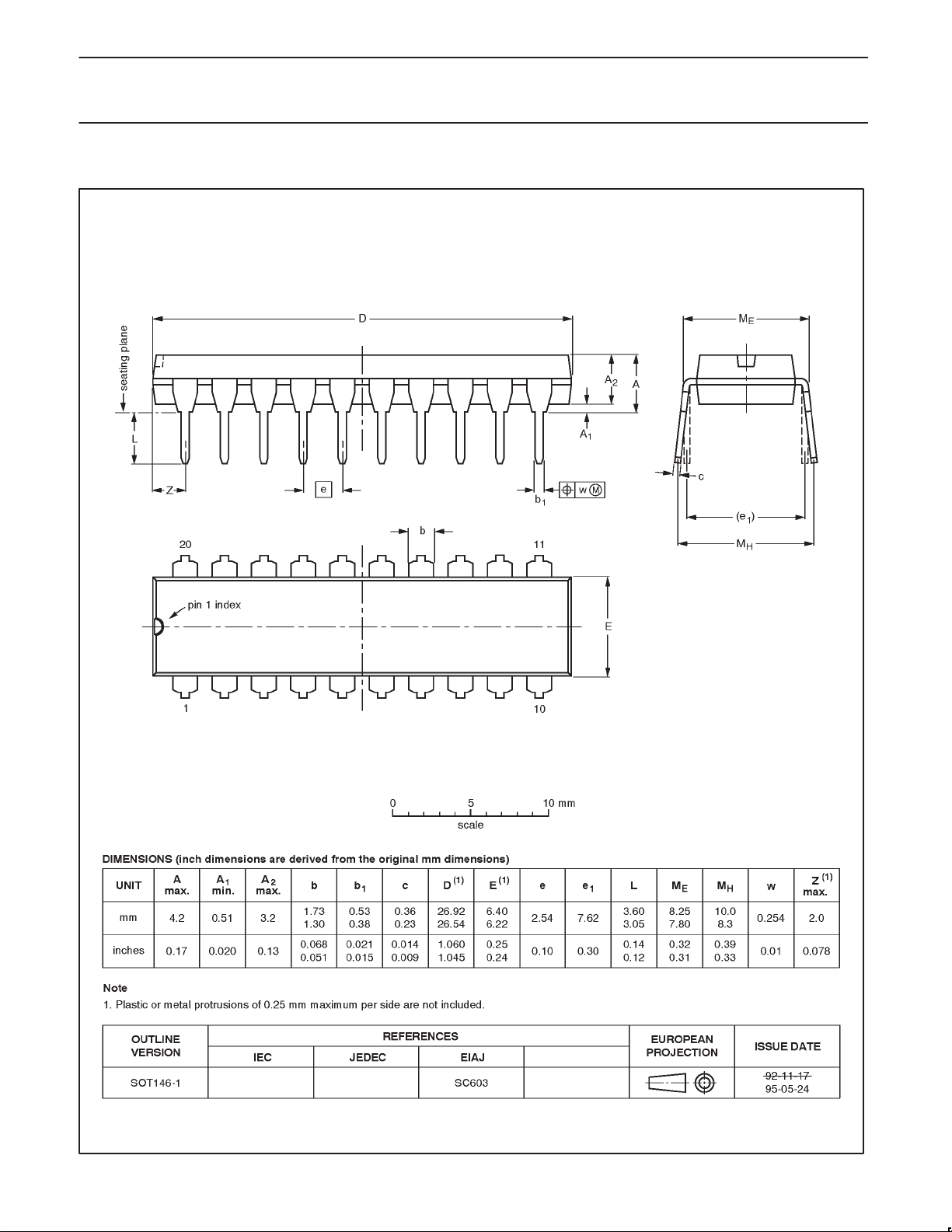
20-Pin Plastic Dual In-Line Package (DIP) –40 to +85°C SA615N SOT146-1
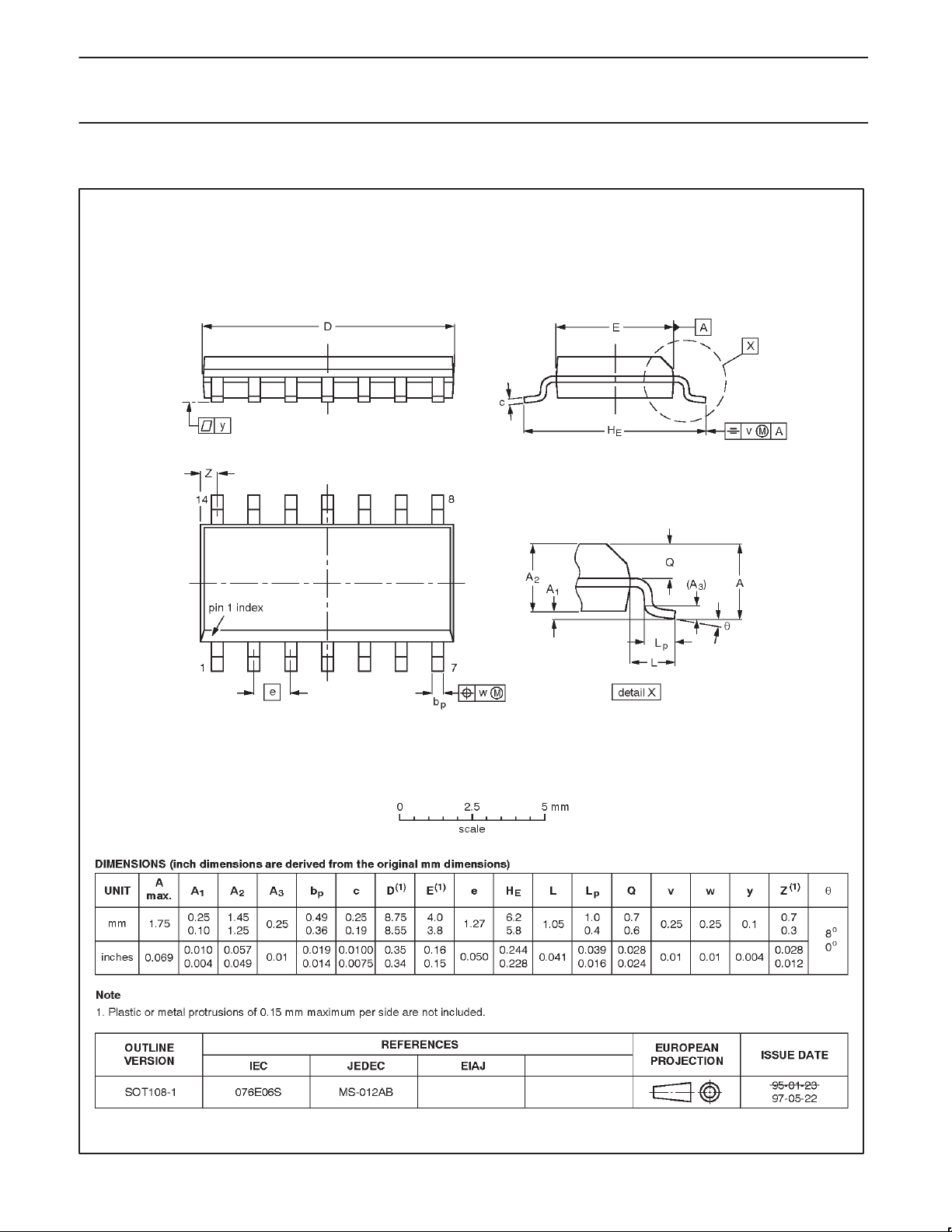
20-Pin Plastic Small Outline Large (SOL) package –40 to +85°C SA615D SOT108-1
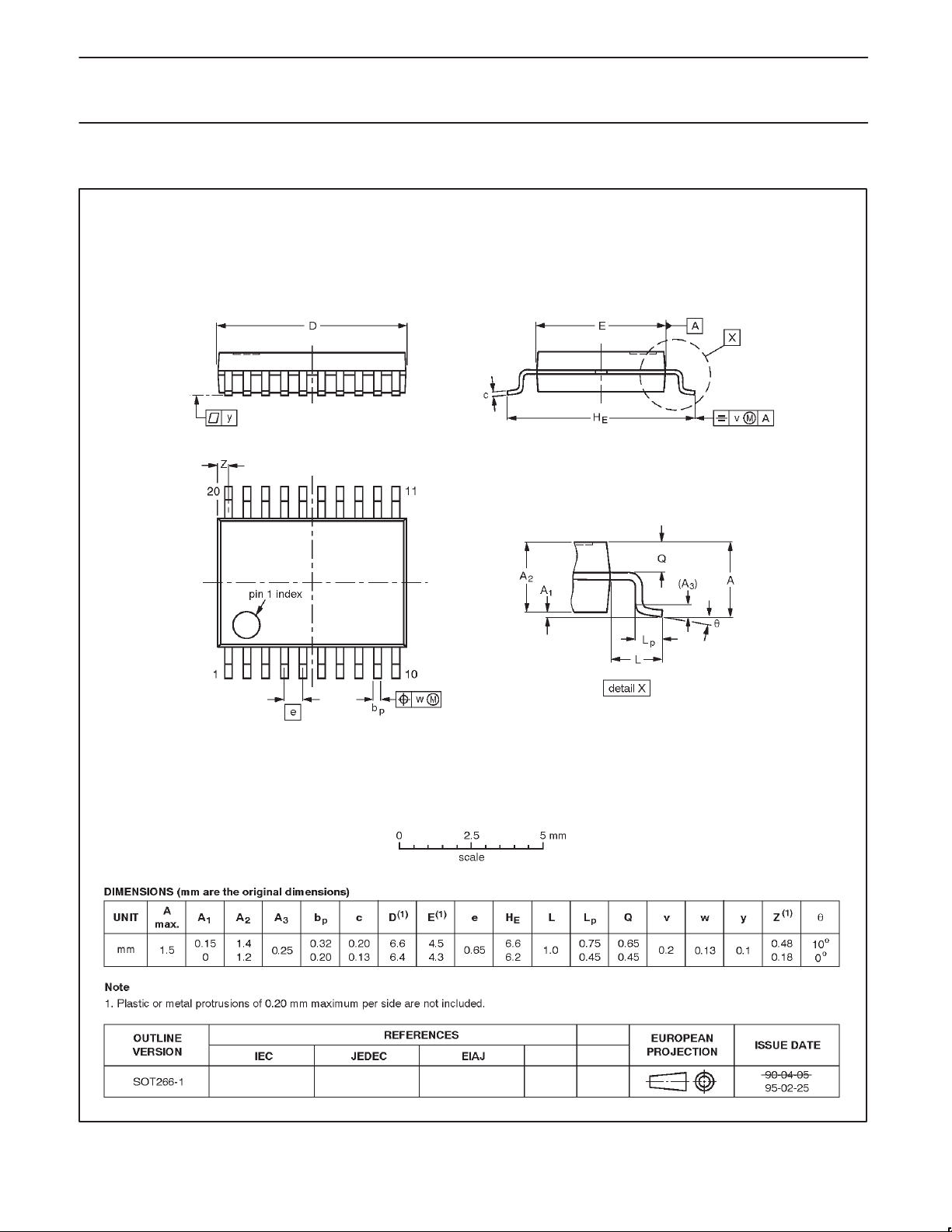
20-Pin Plastic Shrink Small Outline Package (SSOP) –40 to +85°C SA615DK SOT266-1
1997 Nov 07 853-1402 18665
2
Page 3

Philips Semiconductors Product specification
SA615High performance low power mixer FM IF system
BLOCK DIAGRAM
20 19 18 17 16 15 14 13 12 11
IF
AMP
OSCILLATOR
EB
RSSI
LIMITER
10987654321
SR00342
Figure 2. Block Diagram
ABSOLUTE MAXIMUM RATINGS
SYMBOL PARAMETER RATING UNITS
T
V
θ
CC
STG
T
A
JA
Single supply voltage 9 V
Storage temperature range –65 to +150 °C
Operating ambient temperature range SA615 –40 to +85 °C
Thermal impedance D package
N package
SSOP package
90
75
117
°C/W
DC ELECTRICAL CHARACTERISTICS
VCC = +6V, TA = 25°C; unless otherwise stated.
LIMITS
SYMBOL PARAMETER TEST CONDITIONS SA615 UNITS
MIN TYP MAX
V
I
Power supply voltage range 4.5 8.0 V
CC
DC current drain 5.7 7.4 mA
CC
Mute switch input threshold (ON) 1.7 V
(OFF) 1.0 V
1997 Nov 07
3
Page 4

Philips Semiconductors Product specification
SA615High performance low power mixer FM IF system
AC ELECTRICAL CHARACTERISTICS
TA = 25°C; VCC = +6V, unless otherwise stated. RF frequency = 45MHz + 14.5dBV RF input step–up; IF frequency = 455kHz; R17 = 5.1k; RF
level = –45dBm; FM modulation = 1kHz with +
Test circuit Figure 3. The parameters listed below are tested using automatic test equipment to assure consistent electrical characterristics.
The limits do not represent the ultimate performance limits of the device. Use of an optimized RF layout will improve many of the listed
parameters.
SYMBOL PARAMETER TEST CONDITIONS SA615 UNITS
Mixer/Osc section (ext LO = 300mV)
f
Input signal frequency 500 MHz
IN
f
OSC
Crystal oscillator frequency 150 MHz
Noise figure at 45MHz 5.0 dB
Third-order input intercept point f1 = 45.00; f2 = 45.06MHz -12 dBm
Conversion power gain Matched 14.5dBV step-up 8.0 13 dB
RF input resistance Single-ended input 3.0 4.7 kΩ
RF input capacitance 3.5 4.0 pF
Mixer output resistance (Pin 20) 1.25 1.50 kΩ
IF section
IF amp gain 50Ω source 39.7 dB
Limiter gain 50Ω source 62.5 dB
Input limiting -3dB, R17 = 5.1k T est at Pin 18 -109 dBm
AM rejection 80% AM 1kHz 25 33 43 dB
Audio level, R10 = 100k 15nF de-emphasis 60 150 260
Unmuted audio level, R11 = 100k 150pF de-emphasis 530 mV
SINAD sensitivity RF level -118dB 12 dB
THD Total harmonic distortion -30 -42 dB
S/N Signal-to-noise ratio No modulation for noise 68 dB
IF RSSI output, R9 = 100kΩ
RSSI range R9 = 100kΩ Pin 16 80 dB
RSSI accuracy R9 = 100kΩ Pin 16 +2 dB
IF input impedance 1.40 1.6 kΩ
IF output impedance 0.85 1.0 kΩ
Limiter intput impedance 1.40 1.6 kΩ
Unmuted audio output resistance 58 kΩ
Muted audio output resistance 58 kΩ
RF/IF section (int LO)
Unmuted audio level 4.5V = VCC, RF level = -27dBm 450
System RSSI output 4.5V = VCC, RF level = -27dBm 4.3 V
NOTE:
1. The generator source impedance is 50Ω, but the SA615 input impedance at Pin 18 is 1500Ω. As a result, IF level refers to the actual signal
that enters the SA615 input (Pin 8) which is about 21dB less than the ”available power” at the generator.
8kHz peak deviation. Audio output with C-message weighted filter and de-emphasis capacitor.
LIMITS
MIN TYP MAX
50Ω source -1.7 dB
1
IF level = -118dBm 0 160 800 mV
IF level = -68dBm 1.7 2.5 3.3 V
IF level = -18dBm 3.6 4.8 5.8 V
mV
mV
RM
S
RM
S
1997 Nov 07
4
Page 5

Philips Semiconductors Product specification
SA615High performance low power mixer FM IF system
CIRCUIT DESCRIPTION
The SA615 is an IF signal processing system suitable for second IF
or single conversion systems with input frequency as high as 1GHz.
The bandwidth of the IF amplifier is about 40MHz, with 39.7dB(v) of
gain from a 50Ω source. The bandwidth of the limiter is about
28MHz with about 62.5dB(v) of gain from a 50Ω source. However,
the gain/bandwidth distribution is optimized for 455kHz, 1.5kΩ
source applications. The overall system is well-suited to battery
operation as well as high performance and high quality products of
all types.
The input stage is a Gilbert cell mixer with oscillator. Typical mixer
characteristics include a noise figure of 5dB, conversion gain of
13dB, and input third-order intercept of –10dBm. The oscillator will
operate in excess of 1GHz in L/C tank configurations. Hartley or
Colpitts circuits can be used up to 100MHz for xtal configurations.
Butler oscillators are recommended for xtal configurations up to
150MHz.
The output of the mixer is internally loaded with a 1.5kΩ resistor
permitting direct connection to a 455kHz ceramic filter. The input
resistance of the limiting IF amplifiers is also 1.5kΩ. With most
455kHz ceramic filters and many crystal filters, no impedance
matching network is necessary. To achieve optimum linearity of the
log signal strength indicator , there must be a 12dB(v) insertion loss
between the first and second IF stages. If the IF filter or interstage
network does not cause 12dB(v) insertion loss, a fixed or variable
resistor can be added between the first IF output (Pin 16) and the
interstage network.
The signal from the second limiting amplifier goes to a Gilbert cell
quadrature detector . One port of the Gilbert cell is internally driven
by the IF. The other output of the IF is AC-coupled to a tuned
quadrature network. This signal, which now has a 90
relationship to the internal signal, drives the other port of the
multiplier cell.
Overall, the IF section has a gain of 90dB. For operation at
intermediate frequencies greater than 455kHz, special care must be
given to layout, termination, and interstage loss to avoid instability.
The demodulated output of the quadrature detector is available at
two pins, one continuous and one with a mute switch. Signal
attenuation with the mute activated is greater than 60dB. The mute
input is very high impedance and is compatible with CMOS or TTL
levels.
A log signal strength completes the circuitry. The output range is
greater than 90dB and is temperature compensated. This log signal
strength indicator exceeds the criteria for AMPs or TACs cellular
telephone.
NOTE: dB(v) = 20log V
OUT/VIN
° phase
1997 Nov 07
5
Page 6
Philips Semiconductors Product specification
SA615High performance low power mixer FM IF system
–25dB,
Ω PAD
1500/50
50.5
3880
SW9
20
C1
L1
C2
R4
51.1
SW2
R1
C3
R2
R3
45MHZ
MINI–CIRCUIT ZSC2–1B
–10dB,
Ω PAD
50/50
96.5
2430
32.6
C24 C22
FLT1
C23
71.5
–29dB,
929/50
51.5
SW8
C21
19 18 17 16 15 14
IF AMP
MIXER
OSCILLATOR
EMITTER BASE
SW3 SW4SW1
C8
C7
C4
C5
EXT.
LOC
OSC
44.545
L2
R6
178
R7
30.5
X1
C6
45.06
MHZ
Automatic Test Circuit Component List
C1
47pF NPO Ceramic
C2
180pF NPO Ceramic
C5
C6
C7
C8
C9
C10
C11
C12
C13
C14
C15
C17
C18
*NOTE: This value can be reduced when a battery is the power source.
10% Monolithic Ceramic
100nF +
22pF NPO Ceramic
1nF Ceramic
10.0pF NPO Ceramic
10% Monolithic Ceramic
100nF +
µF Tantalum (minimum) *
6.8
100nF +
10% Monolithic Ceramic
10% Ceramic
15nF +
2% N1500 Ceramic
150pF +
10% Monolithic Ceramic
100nF +
10pF NPO Ceramic
100nF +10% Monolithic Ceramic
100nF +
10% Monolithic Ceramic
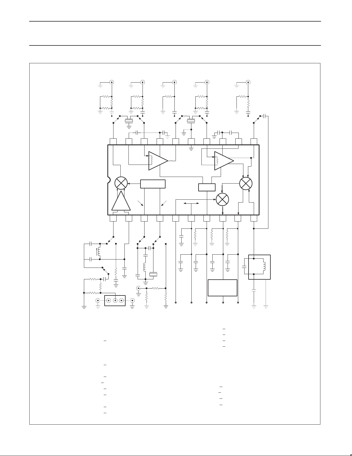
Figure 3. SA615 45MHz Test Circuit (Relays as shown)
R17
5.1k
C9
V
CC
–10.6dB,
50/50
32.8
FLT2
Ω PAD
C20
SW7
700
R8
39.2
MUTE RSSI
C21
C23
C25
C26
Flt 1
Flt 2
IFT 1
L1
L2
X1
R9
R17
R10
R11
C17
–36dB,
156k/50
51.7
Ω PAD
1.3k
C16
C15
Ω PAD
96.5
71.5
C19
SW6 SW5
C18
13 12 11
LIMITER
QUAD
DETECTOR
RSSI
MUTE
SWITCH
10987654321
R9 R10 R11
C13C12C11C10
IFT1
C26
”C” WEIGHTED
AUDIO
MEASUREMENT
CIRCUIT
OUTPUT
100nF +
100nF +
100nF +
390pF +
AUDIO UNMUTED
AUDIO
10% Monolithic Ceramic
10% Monolithic Ceramic
10% Monolithic Ceramic
10% Monolithic Ceramic
C14
Ceramic Filter Murata SFG455A3 or equiv
Ceramic Filter Murata SFG455A3 or equiv
455kHz 270µH TOKO #303LN-1129
300nH TOKO #5CB-1055Z
0.8µH TOKO 292CNS–T1038Z
44.545MHz Crystal ICM4712701
1% 1/4W Metal Film
100k +
5.1k +
5% 1/4W Carbon Composition
1% 1/4W Metal Film (optional)
100k +
100k +
1% 1/4W Metal Film (optional)
SR00343
1997 Nov 07
6
Page 7
Philips Semiconductors Product specification
SA615High performance low power mixer FM IF system
45MHz
INPUT
FLT1
C23
20
19 18 17 16 15 14
IF AMP
MIXER
OSCILLATOR
C21
700
R17
5.1k
FLT2
LIMITER
RSSI
C18
C17
13 12 11
QUAD
DETECTOR
MUTE
SWITCH
C15
10987654321
C9
C1
C8
L1
C2
R5
C5
C6
C7
L2
X1
R9 R10 R11
C13C12C11C10
IFT1
C26
C25
C14
1997 Nov 07
MUTE RSSI
Application Component List
47pF NPO Ceramic
C1
C2
180pF NPO Ceramic
C5
C6
C7
C8
C9
C10
C11
C12
C13
C14
C15
C17
C18
*NOTE: This value can be reduced when a battery is the power source.
10% Monolithic Ceramic
100nF +
22pF NPO Ceramic
1nF Ceramic
10.0pF NPO Ceramic
10% Monolithic Ceramic
100nF +
6.8
µF Tantalum (minimum) *
100nF +
10% Monolithic Ceramic
15nF +
10% Ceramic
2% N1500 Ceramic
150pF +
10% Monolithic Ceramic
100nF +
10pF NPO Ceramic
100nF +
10% Monolithic Ceramic
10% Monolithic Ceramic
100nF +
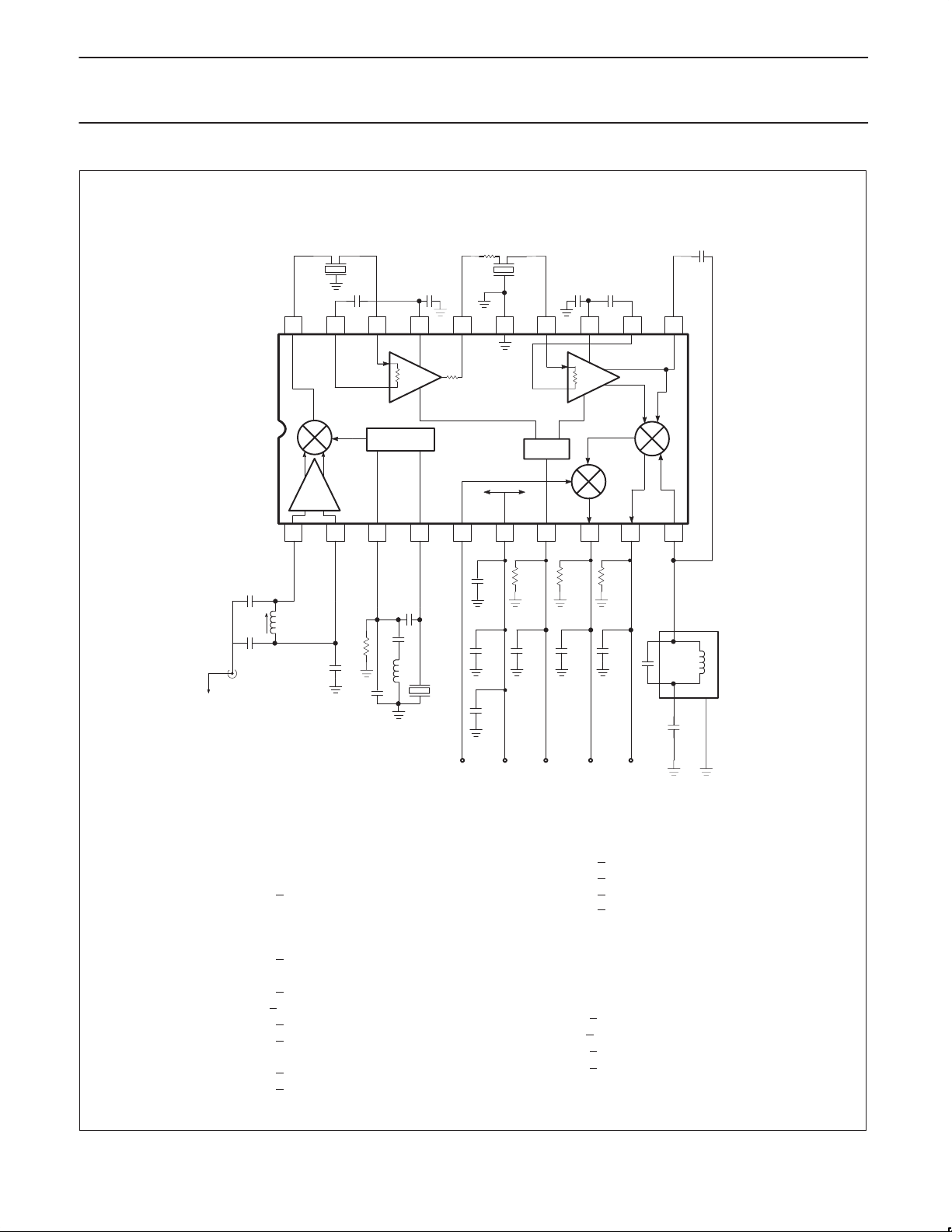
Figure 4. SA615 45MHz Application Circuit
V
CC
NE/SA615N
C21
C23
C25
C26
Flt 1
Flt 2
IFT 1
R17
R10
R11
7
AUDIO UNMUTED
OUTPUT
100nF +
100nF +
100nF +
390pF +
AUDIO
10% Monolithic Ceramic
10% Monolithic Ceramic
10% Monolithic Ceramic
10% Monolithic Ceramic
Ceramic Filter Murata SFG455A3 or equiv
Ceramic Filter Murata SFG455A3 or equiv
455kHz 270µH TOKO #303LN-1129
L1
300nH TOKO #5CB-1055Z
L2
0.8µH TOKO 292CNS–T1038Z
X1
44.545MHz Crystal ICM4712701
R9
100k +
1% 1/4W Metal Film
5% 1/4W Carbon Composition
5.1k +
100k +
1% 1/4W Metal Film (optional)
1% 1/4W Metal Film (optional)
100k +
SR00344
Page 8
Philips Semiconductors Product specification
SA615High performance low power mixer FM IF system
RF GENERATOR
45MHz
V
(+6)
CC
NOTES:
1. C-message: The C-message filter has a peak gain of 100 for accurate measurements. Without the gain, the measurements may be
affected by the noise of the scope and HP339 analyzer.
2. Ceramic filters: The ceramic filters can be 30kHz SFG455A3s made by Murata which have 30kHz IF bandwidth (they come in blue), or
16kHz CFU455Ds, also made by Murata (they come in black). All of our specifications and testing are done with the more wideband filter.
3. RF generator: Set your RF generator at 45.000MHz, use a 1kHz modulation frequency and a 6kHz deviation if you use 16kHz filters, or
8kHz if you use 30kHz filters.
4. Sensitivity: The measured typical sensitivity for 12dB SINAD should be 0.22µV or –120dBm at the RF input.
5. Layout: The layout is very critical in the performance of the receiver. We highly recommend our demo board layout.
6. RSSI: The smallest RSSI voltage (i.e., when no RF input is present and the input is terminated) is a measure of the quality of the layout and
design. If the lowest RSSI voltage is 250mV or higher, it means the receiver is in regenerative mode. In that case, the receiver sensitivity
will be worse than expected.
7. Supply bypass and shielding: All of the inductors, the quad tank, and their shield must be grounded. A 10–15µF or higher value tantalum
capacitor on the supply line is essential. A low frequency ESR screening test on this capacitor will ensure consistent good sensitivity in
production. A 0.1µF bypass capacitor on the supply pin, and grounded near the 44.545MHz oscillator improves sensitivity by 2–3dB.
8. R5 can be used to bias the oscillator transistor at a higher current for operation above 45MHz. Recommended value is 22kΩ, but should not
be below 10kΩ.
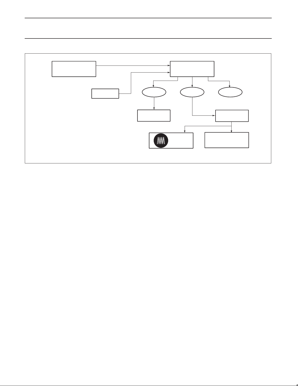
Figure 5. SA615 Application Circuit Test Set Up
RSSI AUDIO DATA
DC VOLTMETER
SA615 DEM0–BOARD
SCOPE
HP339A DISTORTION
C–MESSAGE
ANALYZER
SR00345
1997 Nov 07
8
Page 9
Philips Semiconductors Product specification
SA615High performance low power mixer FM IF system
20
AUDIO REF = 174mV
0
–20
–40
RELATIVE TO AUDIO OUTPUT (dB)
–60
–80
RSSI
(Volts)
–100
–130 –110 –90 –70 –50 –30 –10 10
RF INPUT LEVEL (dBm)
RMS
THD NOISE
AM (80%)
NOISE
RF = 45MHz
IF = 455kHz
VCC = 6V
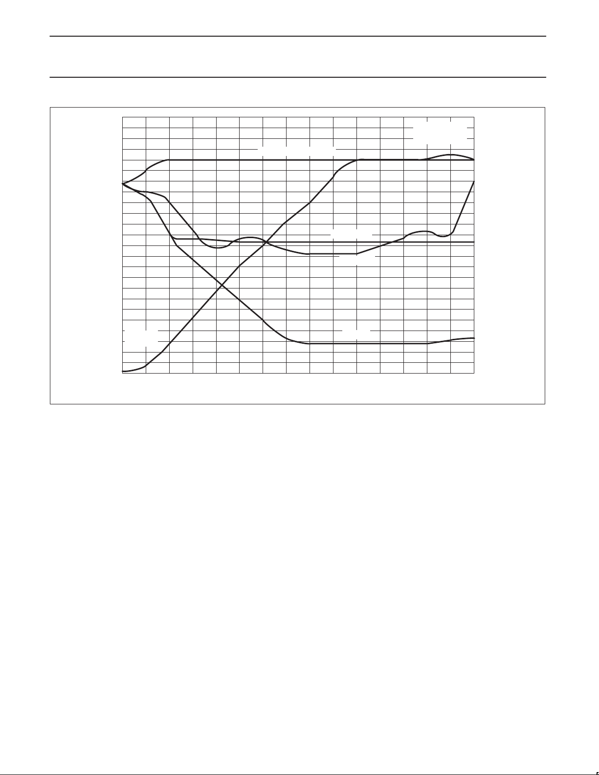
Figure 6. SA615 Application Board at 25°C
5
4
3
2
1
0
SR00346
RSSI
(Volts)
1997 Nov 07
9
Page 10
Philips Semiconductors Product specification
SA615High performance low power mixer FM IF system
DIP20: plastic dual in-line package; 20 leads (300 mil) SOT146-1
1997 Nov 07
10
Page 11
Philips Semiconductors Product specification
SA615High performance low power mixer FM IF system
SO14: plastic small outline package; 14 leads; body width 3.9 mm SOT108-1
1997 Nov 07
11
Page 12
Philips Semiconductors Product specification
SA615High performance low power mixer FM IF system
SSOP20: plastic shrink small outline package; 20 leads; body width 4.4 mm SOT266-1
1997 Nov 07
12
Page 13

Philips Semiconductors Product specification
SA615High performance low power mixer FM IF system
NOTES
1997 Nov 07
13
Page 14

Philips Semiconductors Product specification
SA615High performance low power mixer FM IF system
Data sheet status
Data sheet
status
Objective
specification
Preliminary
specification
Product
specification
Product
status
Development
Qualification
Production
Definition
This data sheet contains the design target or goal specifications for product development.
Specification may change in any manner without notice.
This data sheet contains preliminary data, and supplementary data will be published at a later date.
Philips Semiconductors reserves the right to make chages at any time without notice in order to
improve design and supply the best possible product.
This data sheet contains final specifications. Philips Semiconductors reserves the right to make
changes at any time without notice in order to improve design and supply the best possible product.
[1]
[1] Please consult the most recently issued datasheet before initiating or completing a design.
Definitions
Short-form specification — The data in a short-form specification is extracted from a full data sheet with the same type number and title. For
detailed information see the relevant data sheet or data handbook.
Limiting values definition — Limiting values given are in accordance with the Absolute Maximum Rating System (IEC 134). Stress above one
or more of the limiting values may cause permanent damage to the device. These are stress ratings only and operation of the device at these or
at any other conditions above those given in the Characteristics sections of the specification is not implied. Exposure to limiting values for extended
periods may affect device reliability.
Application information — Applications that are described herein for any of these products are for illustrative purposes only. Philips
Semiconductors make no representation or warranty that such applications will be suitable for the specified use without further testing or
modification.
Disclaimers
Life support — These products are not designed for use in life support appliances, devices or systems where malfunction of these products can
reasonably be expected to result in personal injury . Philips Semiconductors customers using or selling these products for use in such applications
do so at their own risk and agree to fully indemnify Philips Semiconductors for any damages resulting from such application.
Right to make changes — Philips Semiconductors reserves the right to make changes, without notice, in the products, including circuits, standard
cells, and/or software, described or contained herein in order to improve design and/or performance. Philips Semiconductors assumes no
responsibility or liability for the use of any of these products, conveys no license or title under any patent, copyright, or mask work right to these
products, and makes no representations or warranties that these products are free from patent, copyright, or mask work right infringement, unless
otherwise specified.
Philips Semiconductors
811 East Arques Avenue
P.O. Box 3409
Sunnyvale, California 94088–3409
Telephone 800-234-7381
Copyright Philips Electronics North America Corporation 1998
All rights reserved. Printed in U.S.A.
Date of release: 05-98
Document order number: 9397 750 03916
1997 Nov 07
14
 Loading...